
Simulation and Design of Three 5G Antennas

Abstract
1. Introduction
2. Materials and Methods
2.1. Theoretical Analysis of Microstrip Antenna Arrays
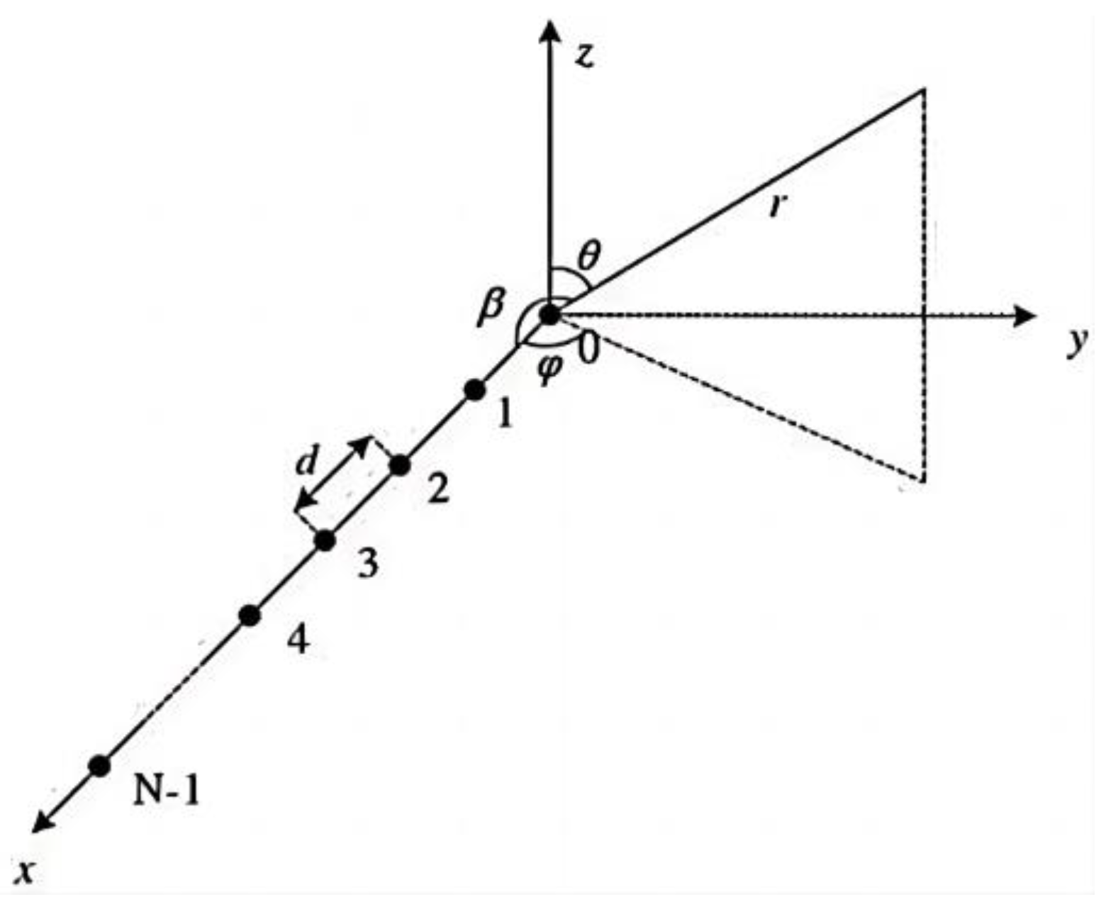
2.1.1. Linear Array
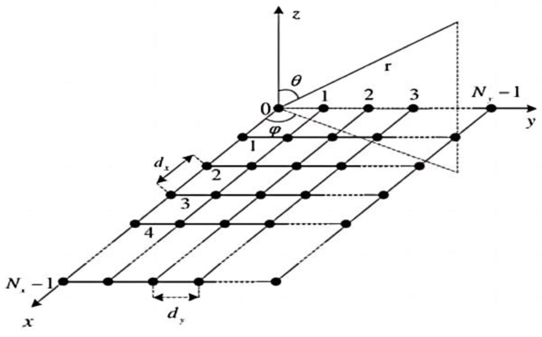
2.1.2. Planar Array
2.2. The Unique Performance Parameters of MIMO Terminal Antennas
2.2.1. Correlation
2.2.2. Average Effective Gain (AEG)
2.2.3. Overall Efficiency
3. Design of 5G Microstrip Array Antennas
3.1. Design and Simulation of Antenna Units
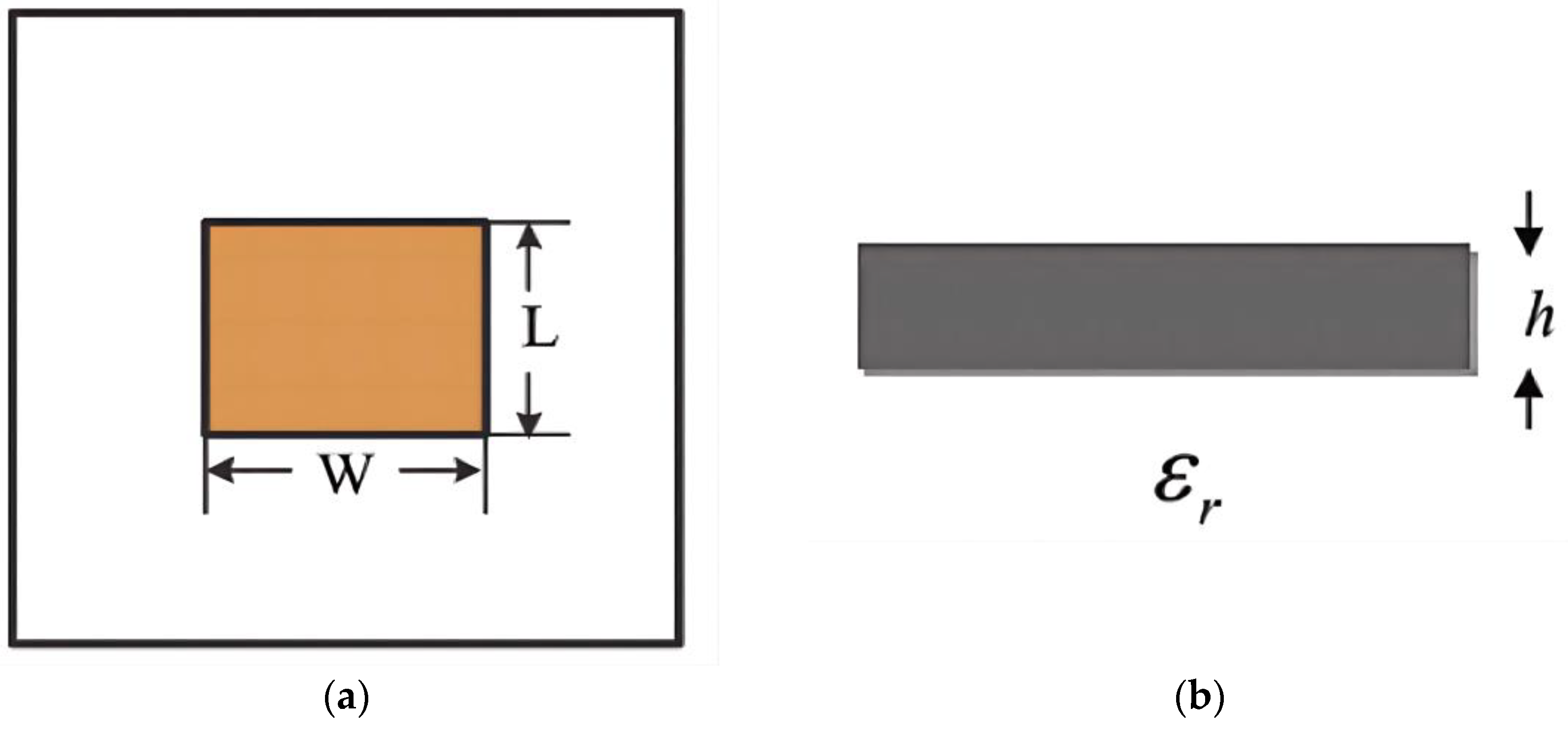
3.1.1. Calculation and Optimization of Antenna Unit Parameters
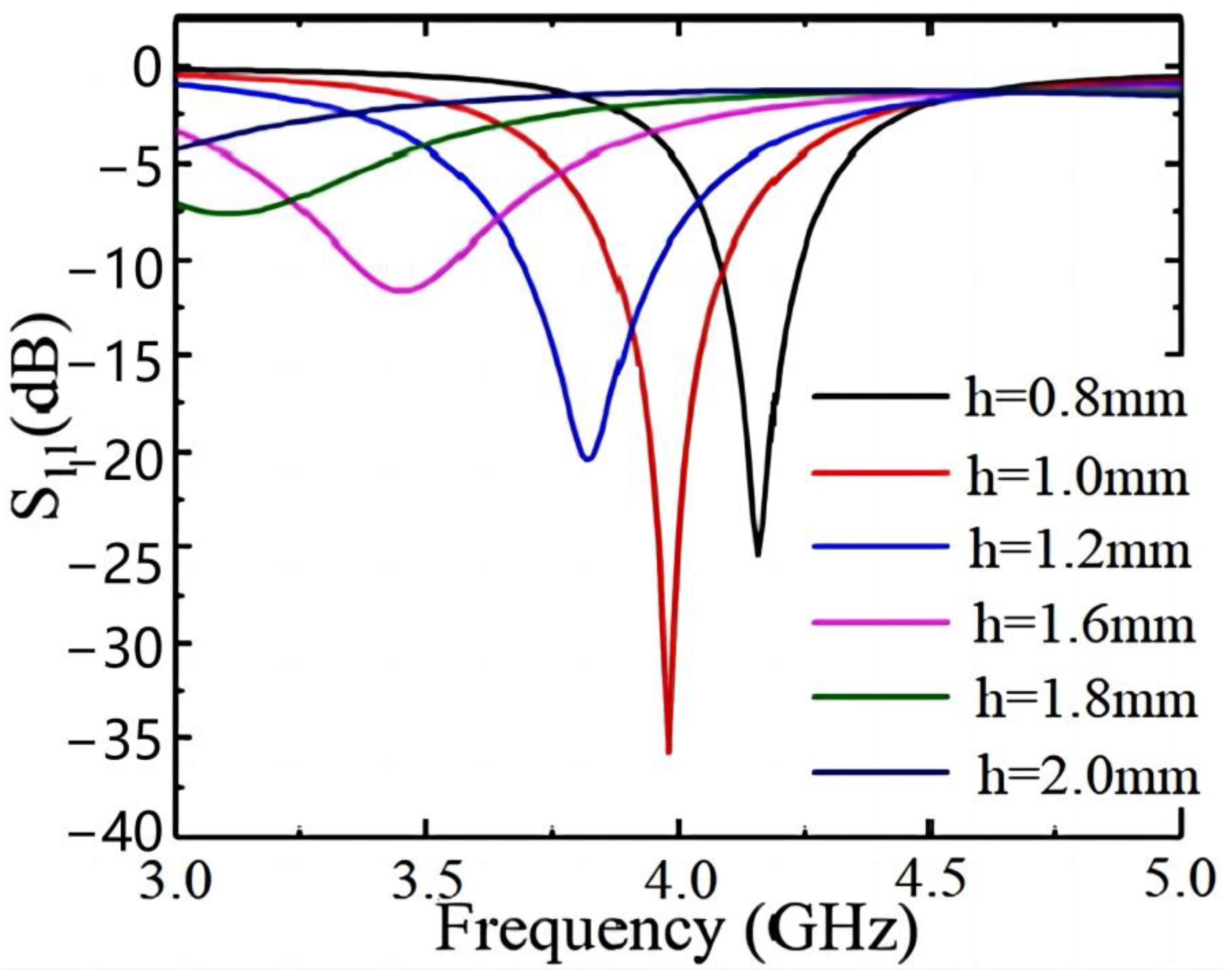
Dielectric Substrate Thickness (h)
Antenna Element Width (W)
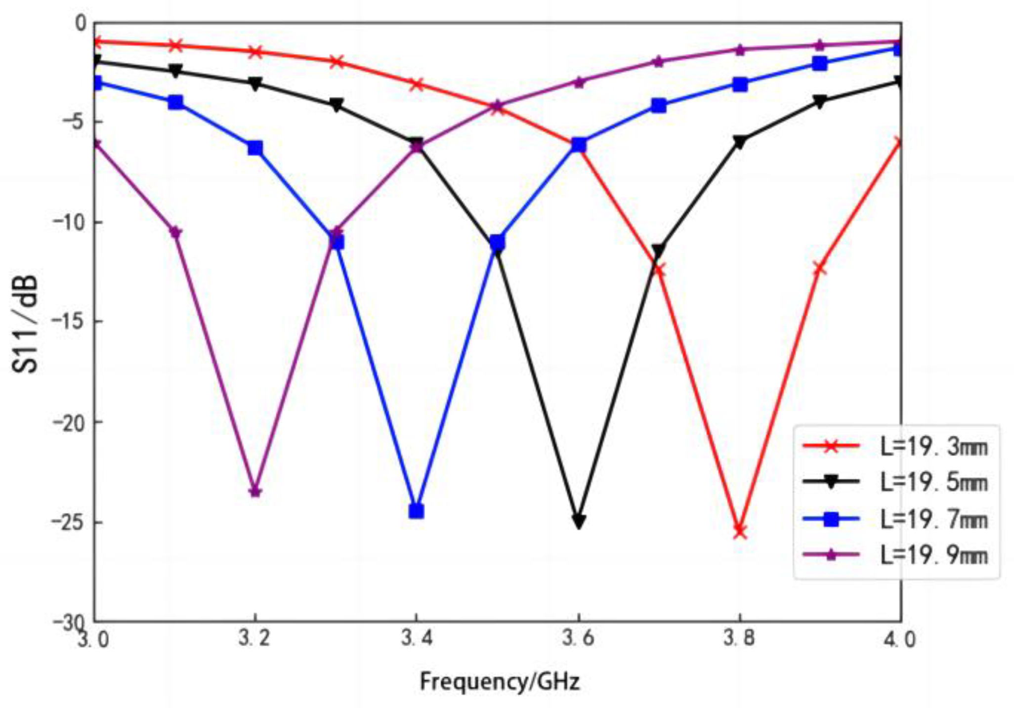
Antenna Element Length (L)
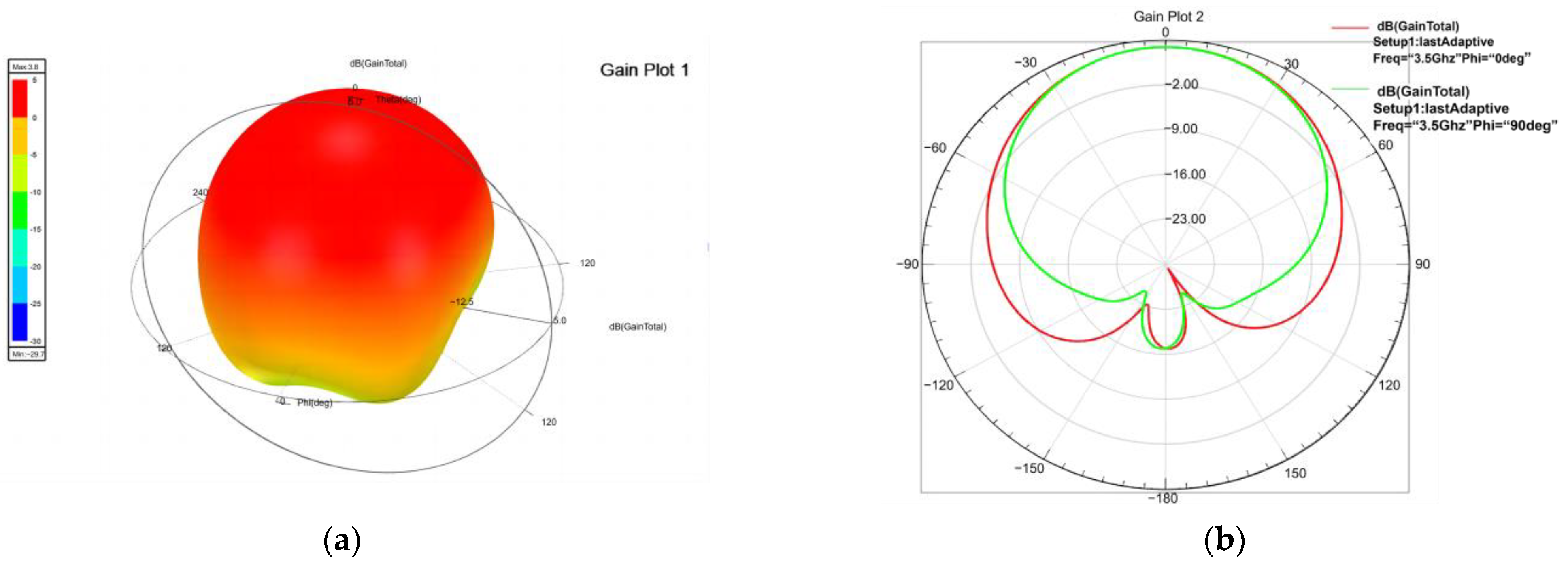
3.1.2. Simulation of Antenna Units
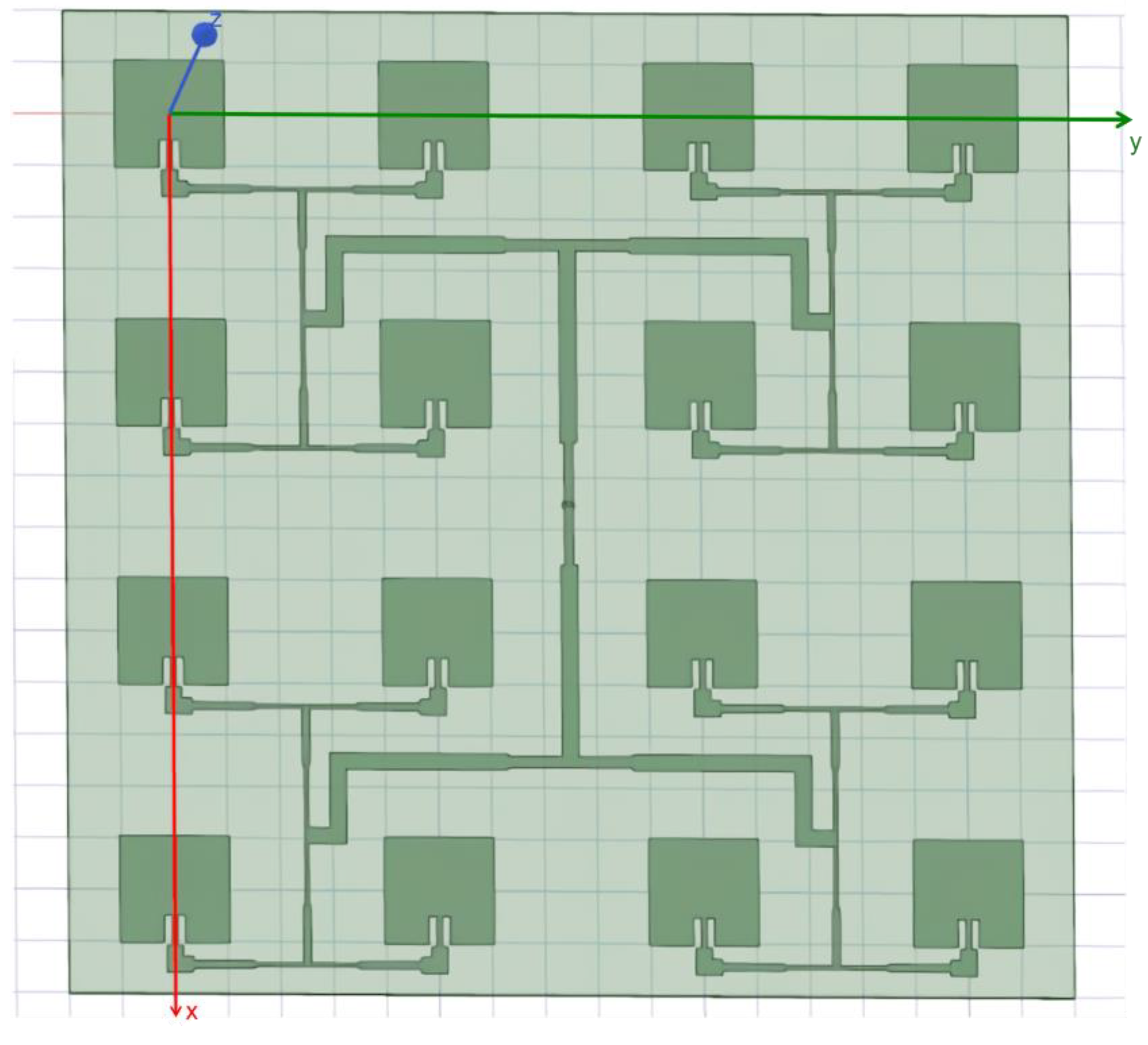
3.2. Design and Simulation of 4 × 4 Antenna Units
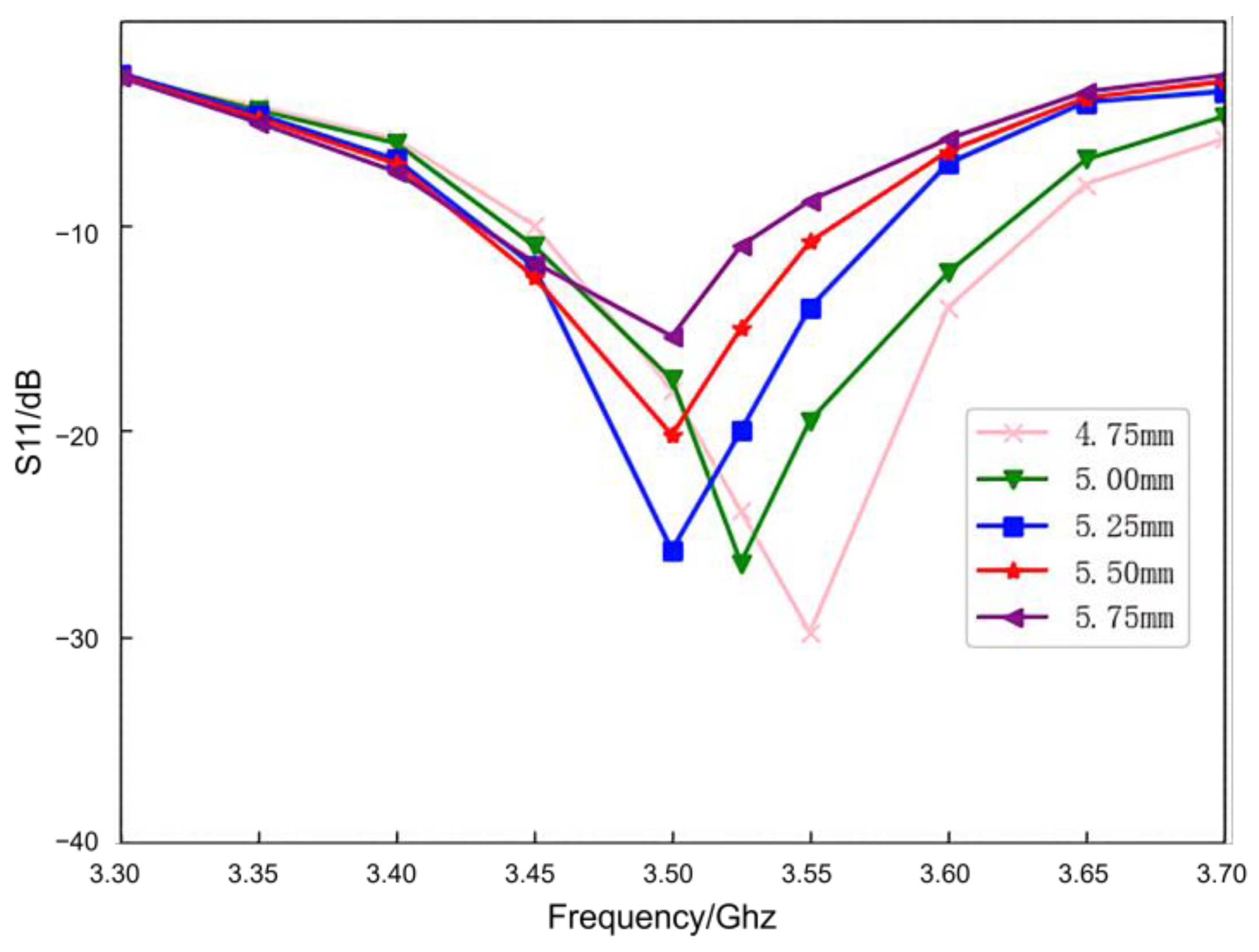
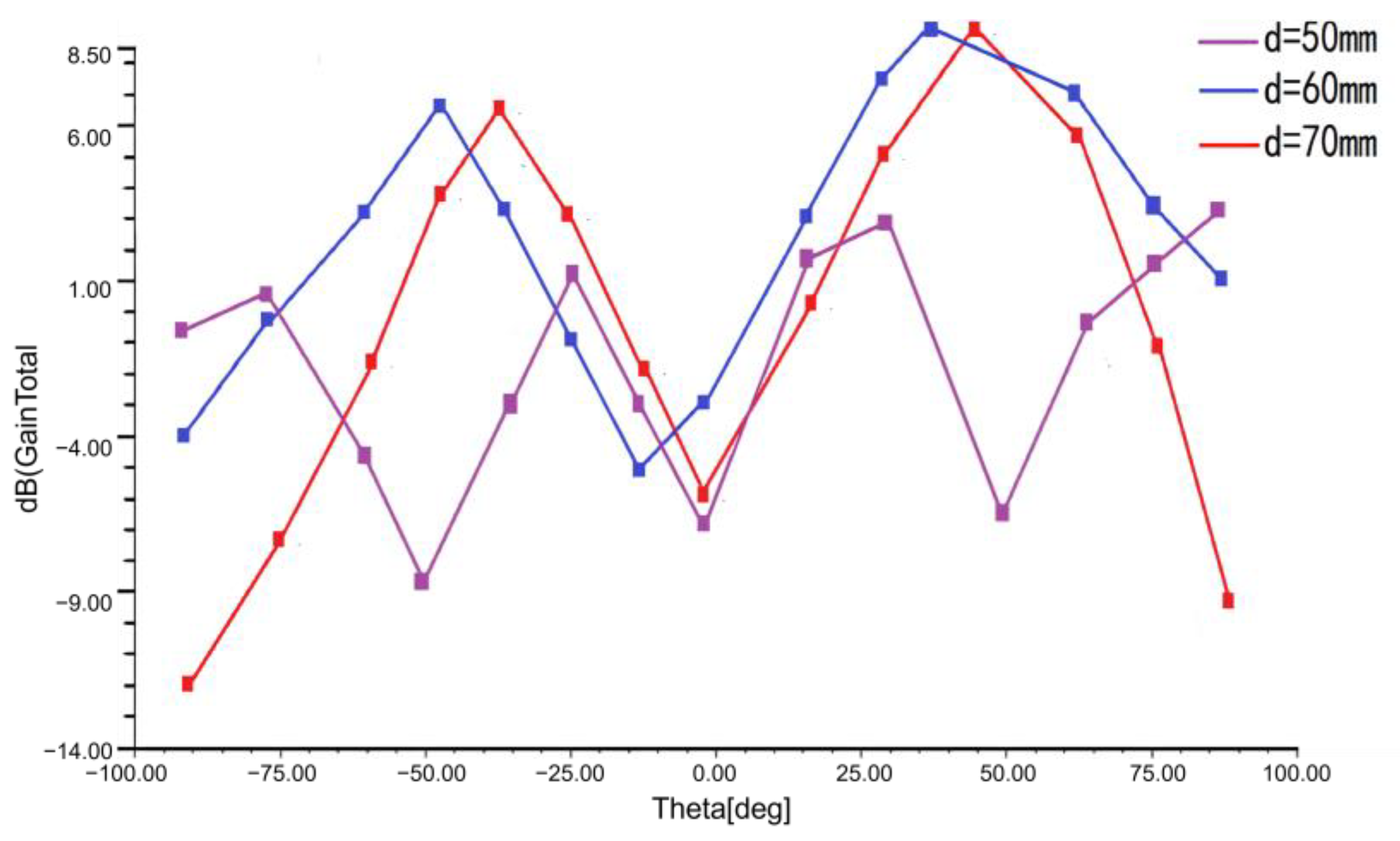
3.2.1. Analysis and Simulation of Element Spacing
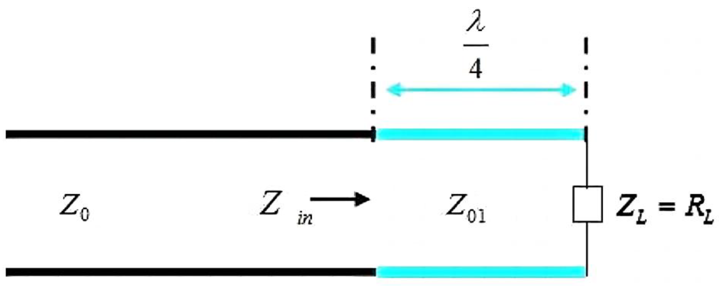
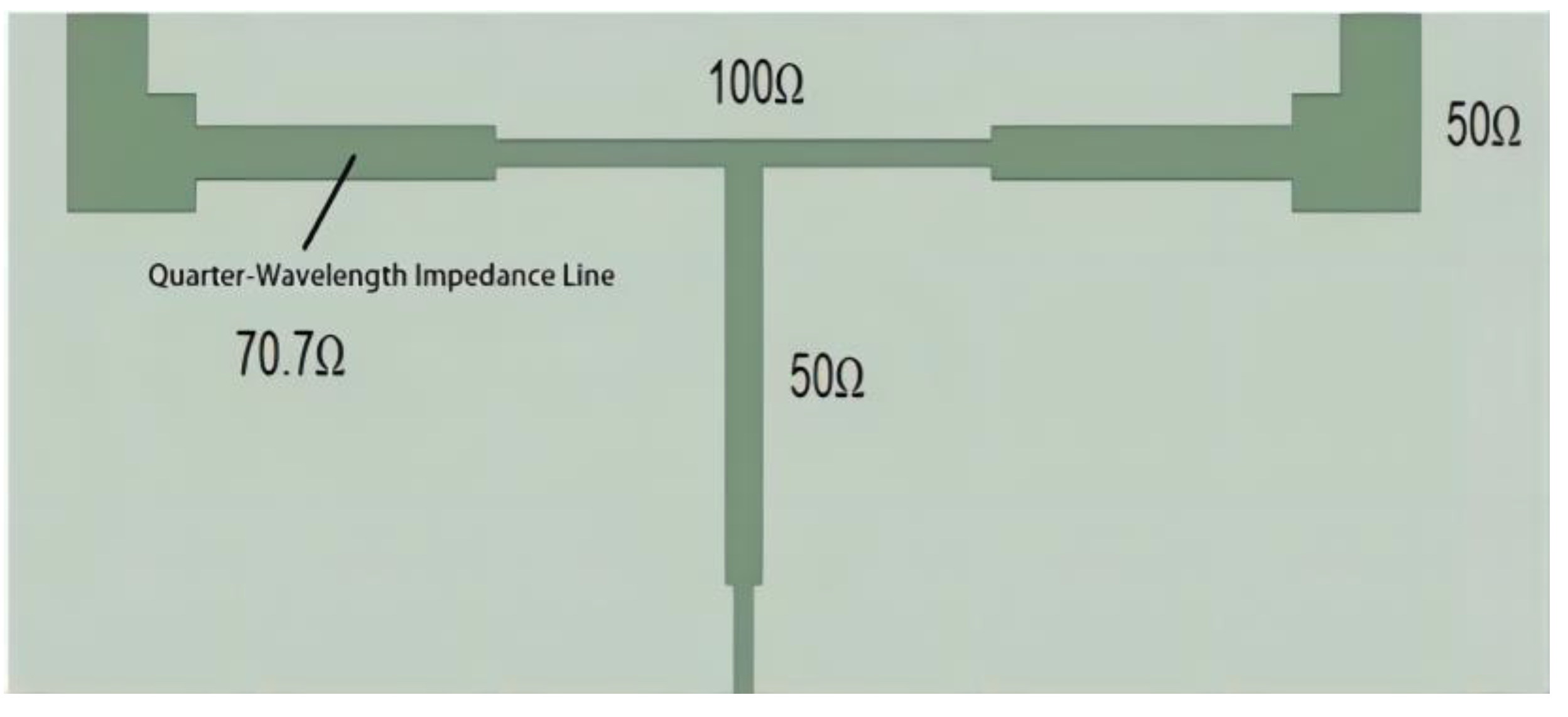
3.2.2. The Design and Simulation of the Feeding Network
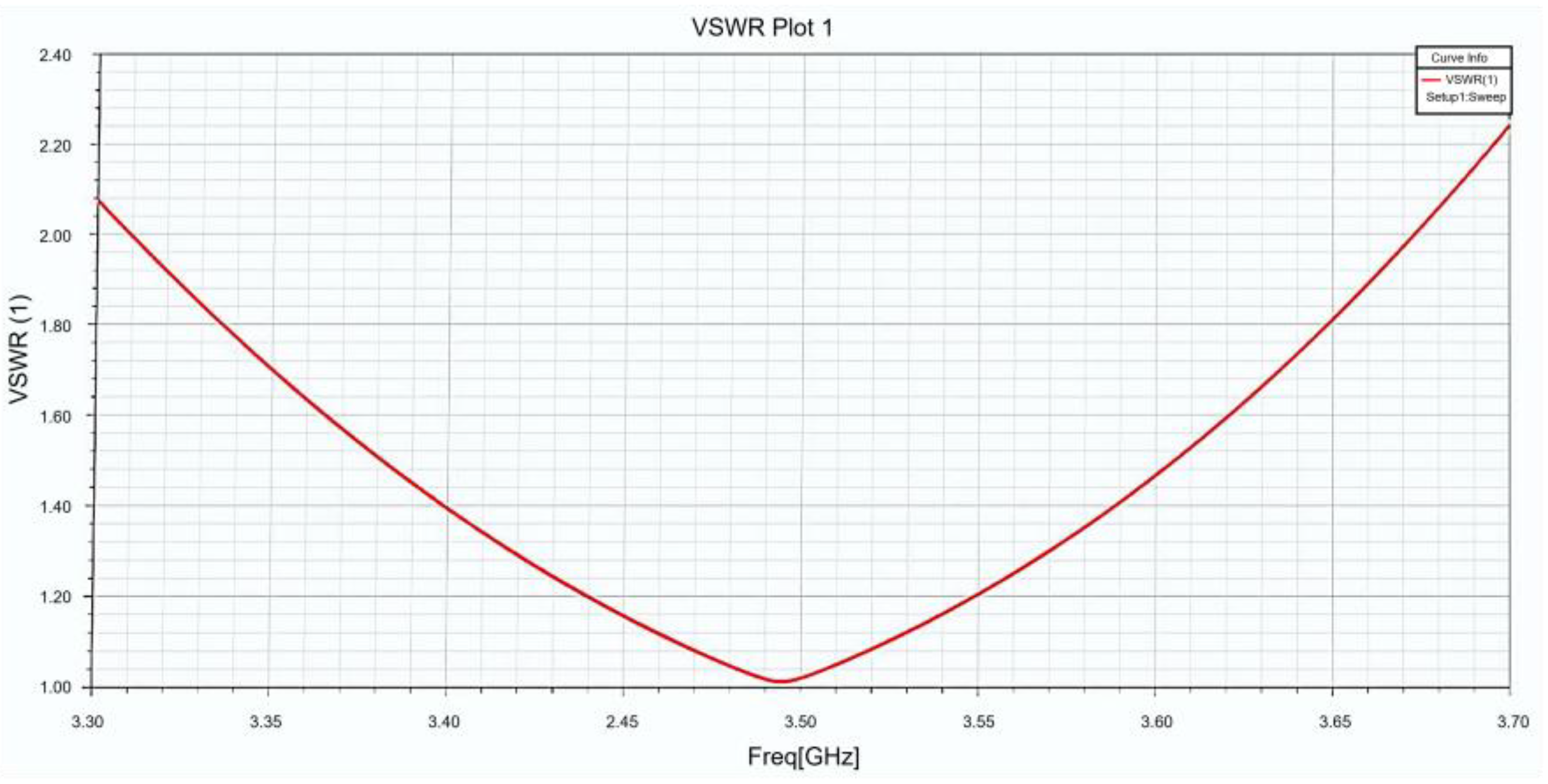
3.2.3. Simulation of a 4 × 4 Array Antenna
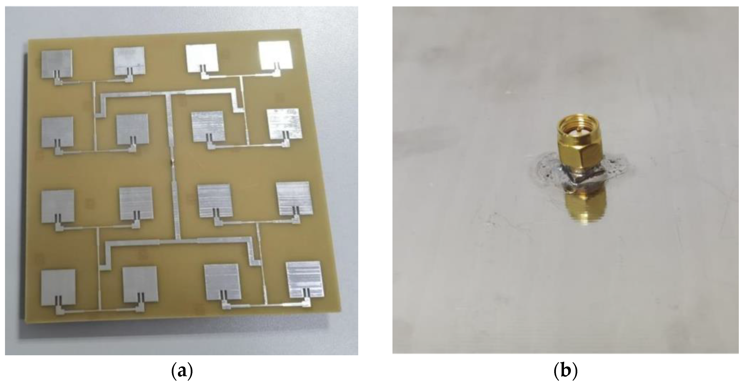
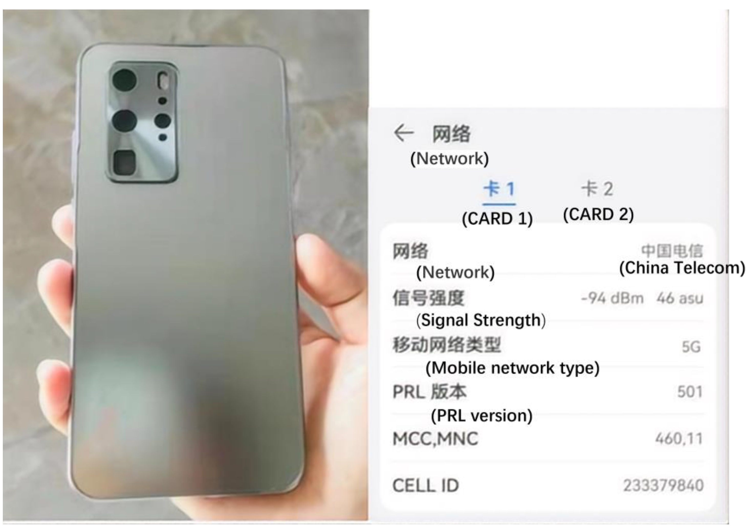
3.2.4. Fabrication of a 4×4 Array Antenna Prototype
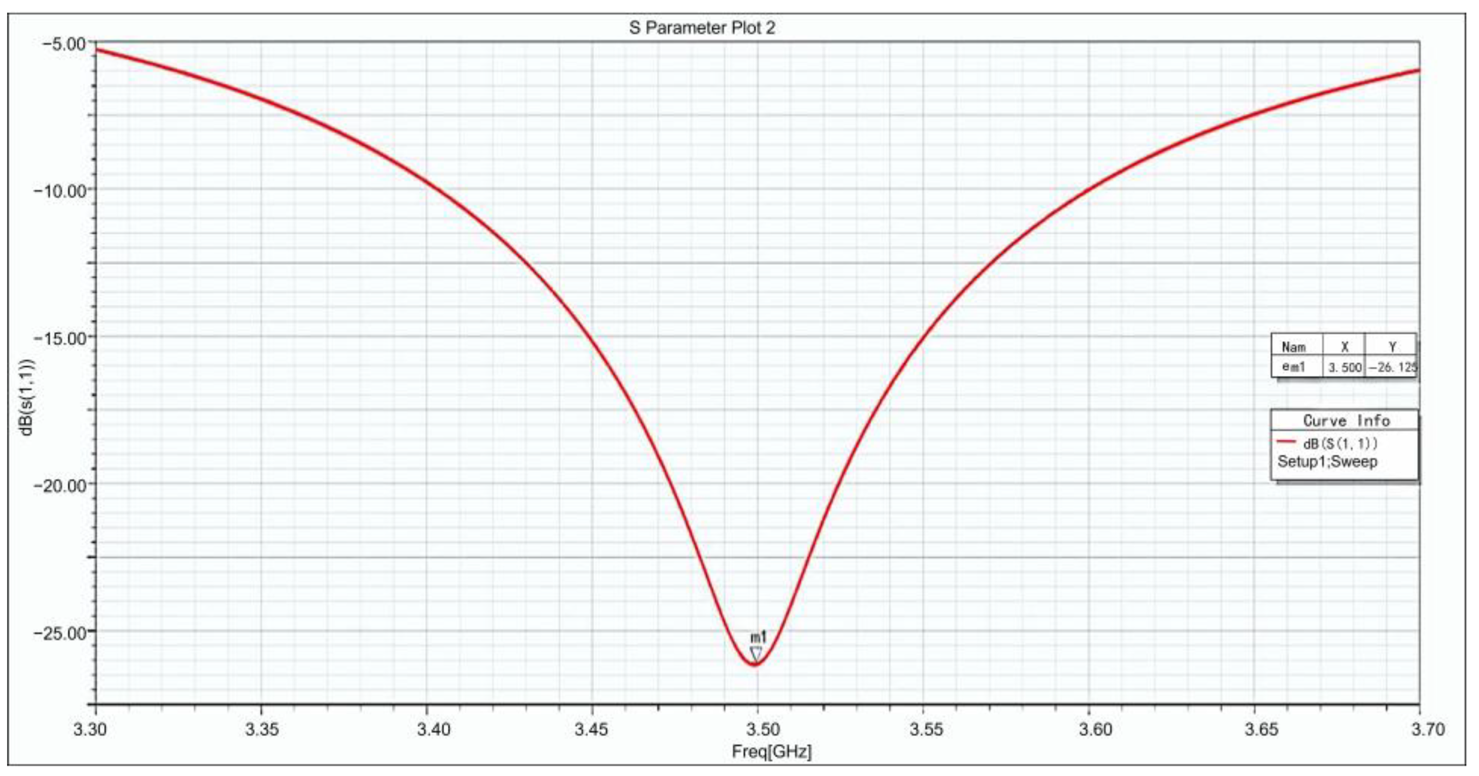
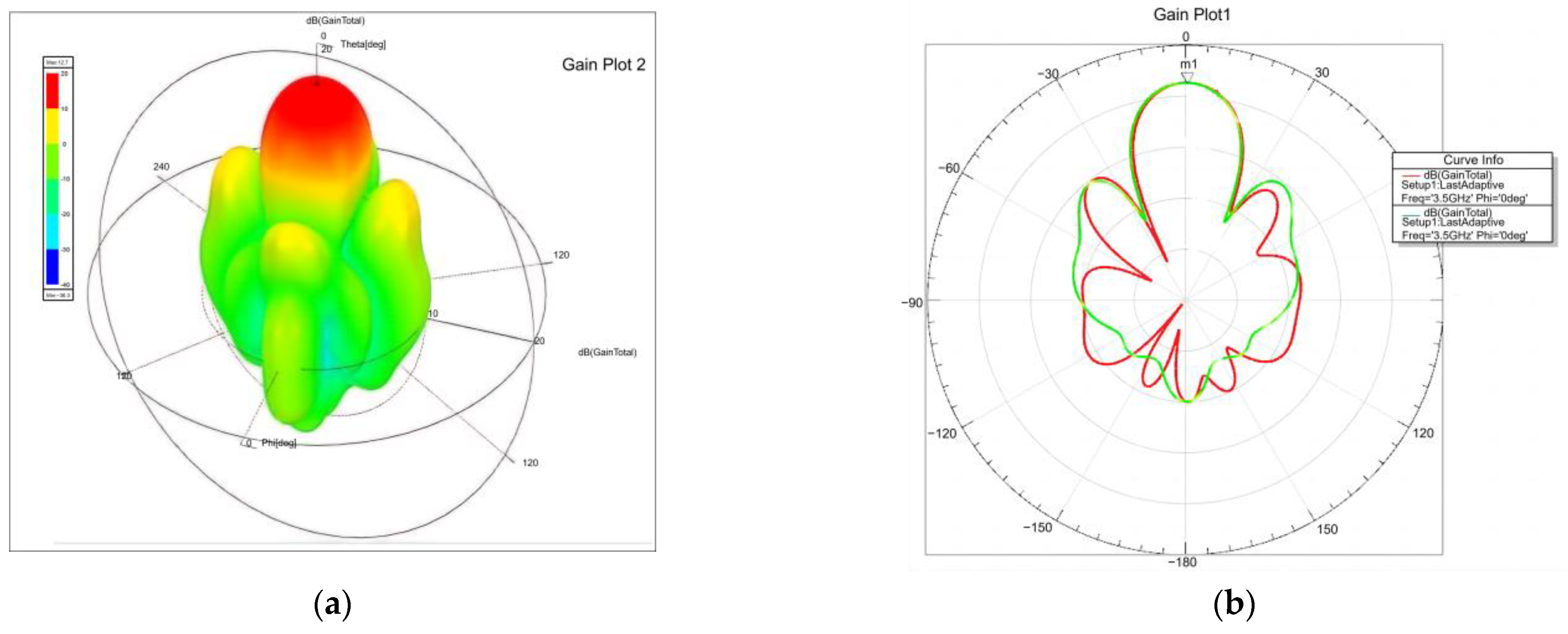
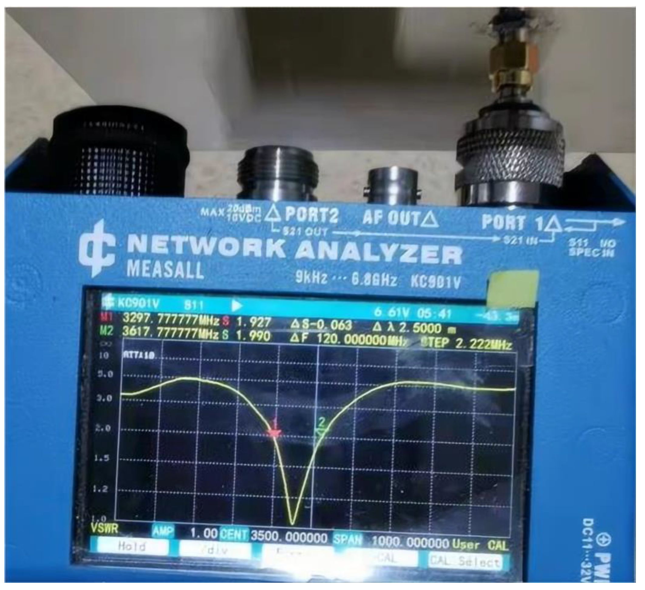
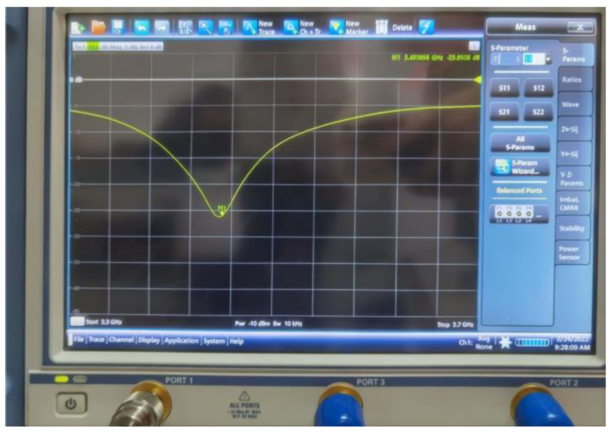
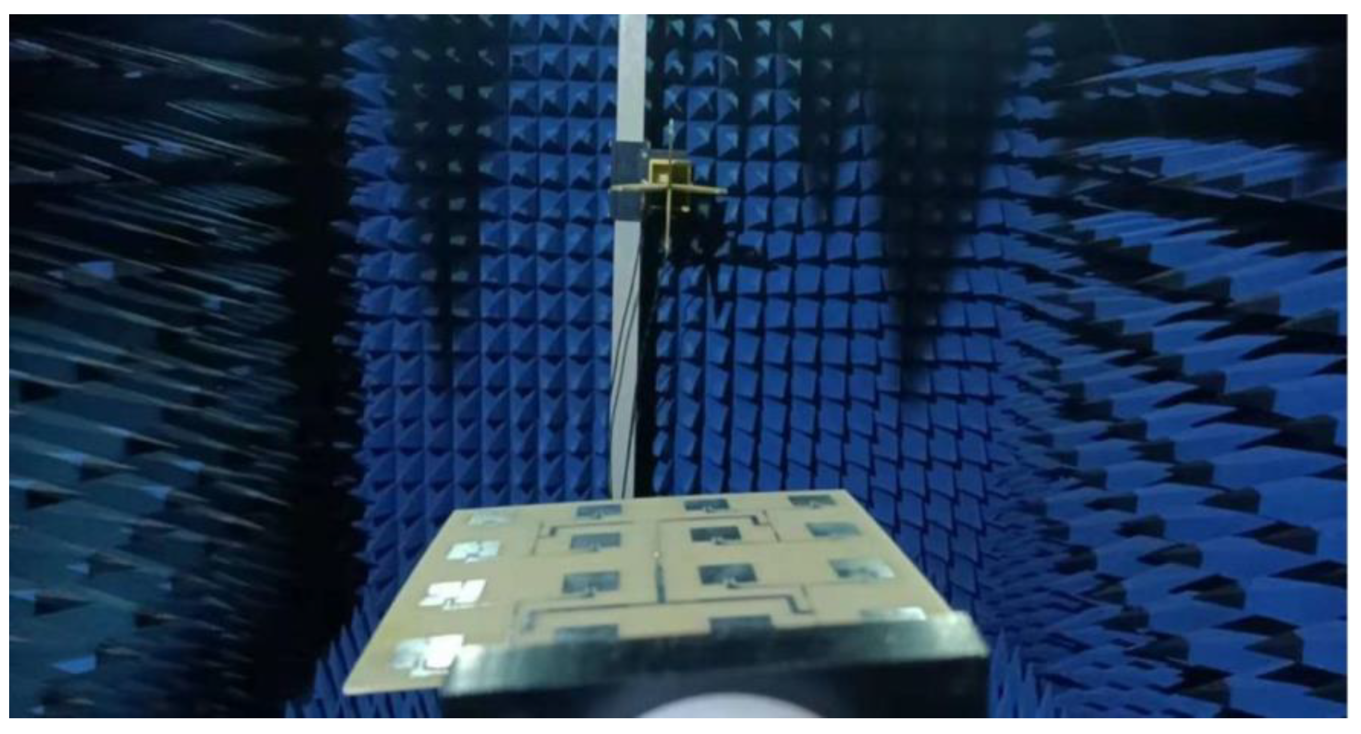
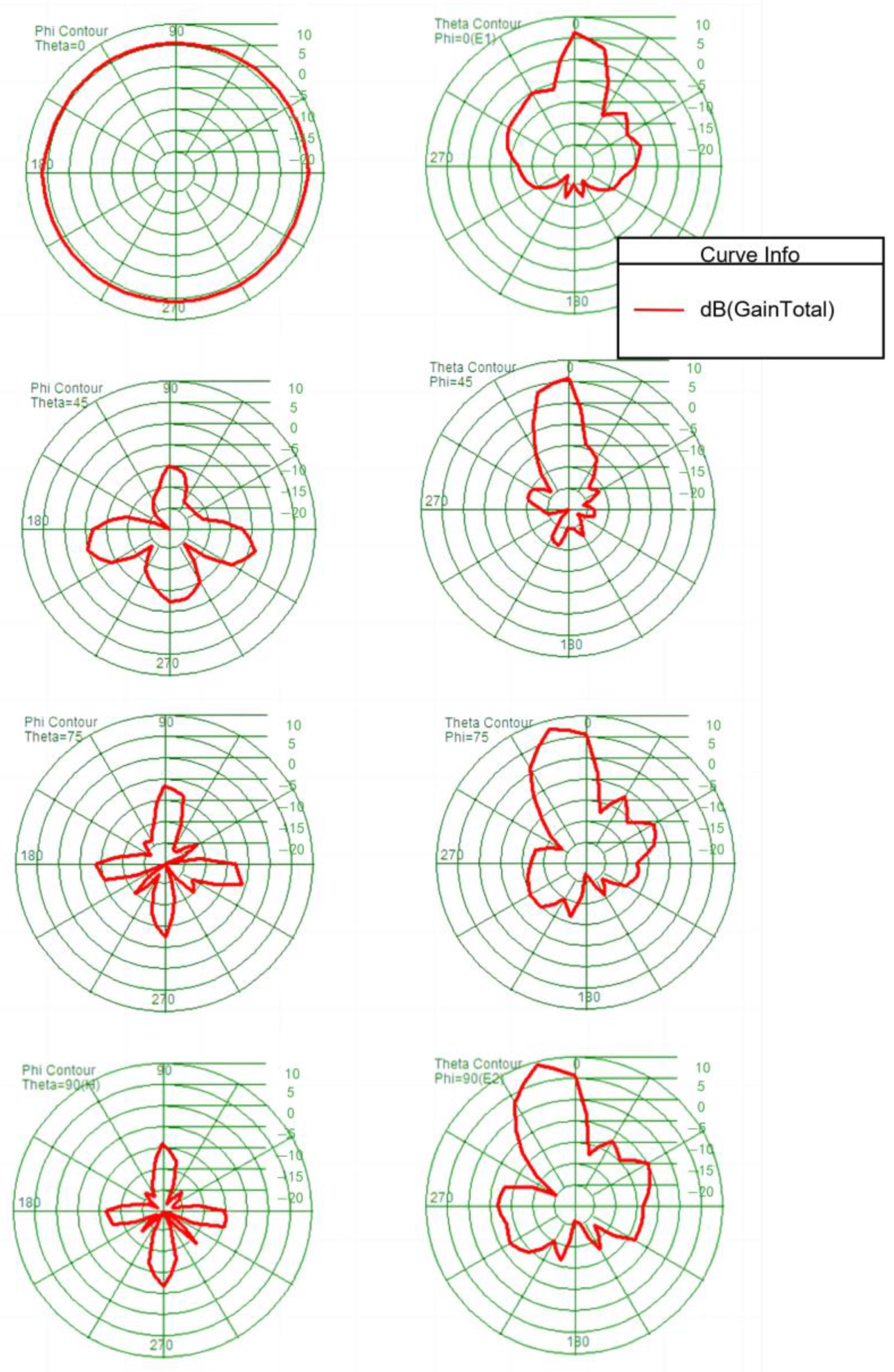
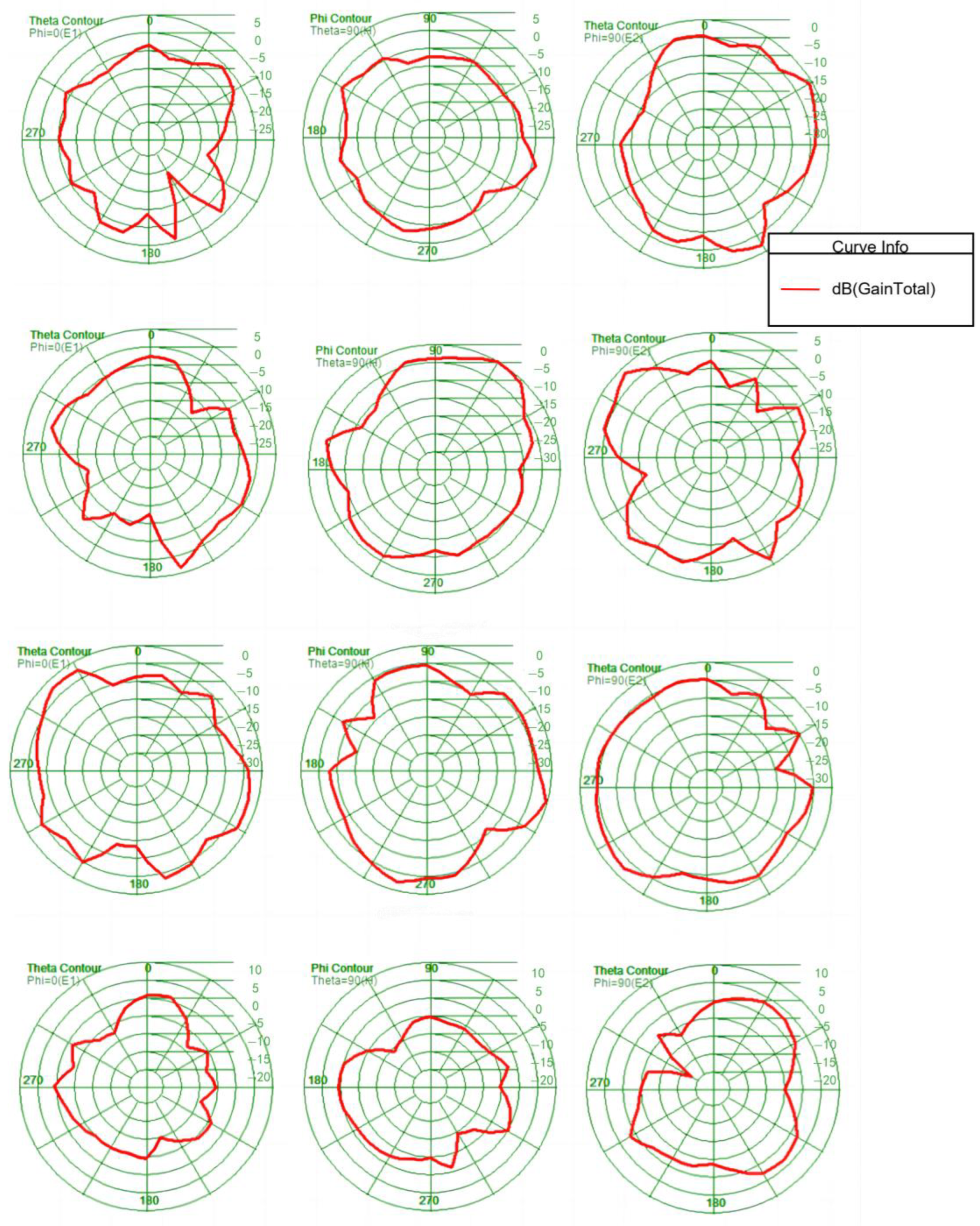
3.2.5. Physical Measurement and Result Analysis
4. Metal Frame Mobile Terminal Dual-Element “Loop-Groove” MIMO Antenna Design
4.1. The Impact of Metal Frame on Mobile Terminals
4.2. The Dual-Element “Loop-Groove” MIMO Antenna Design Process
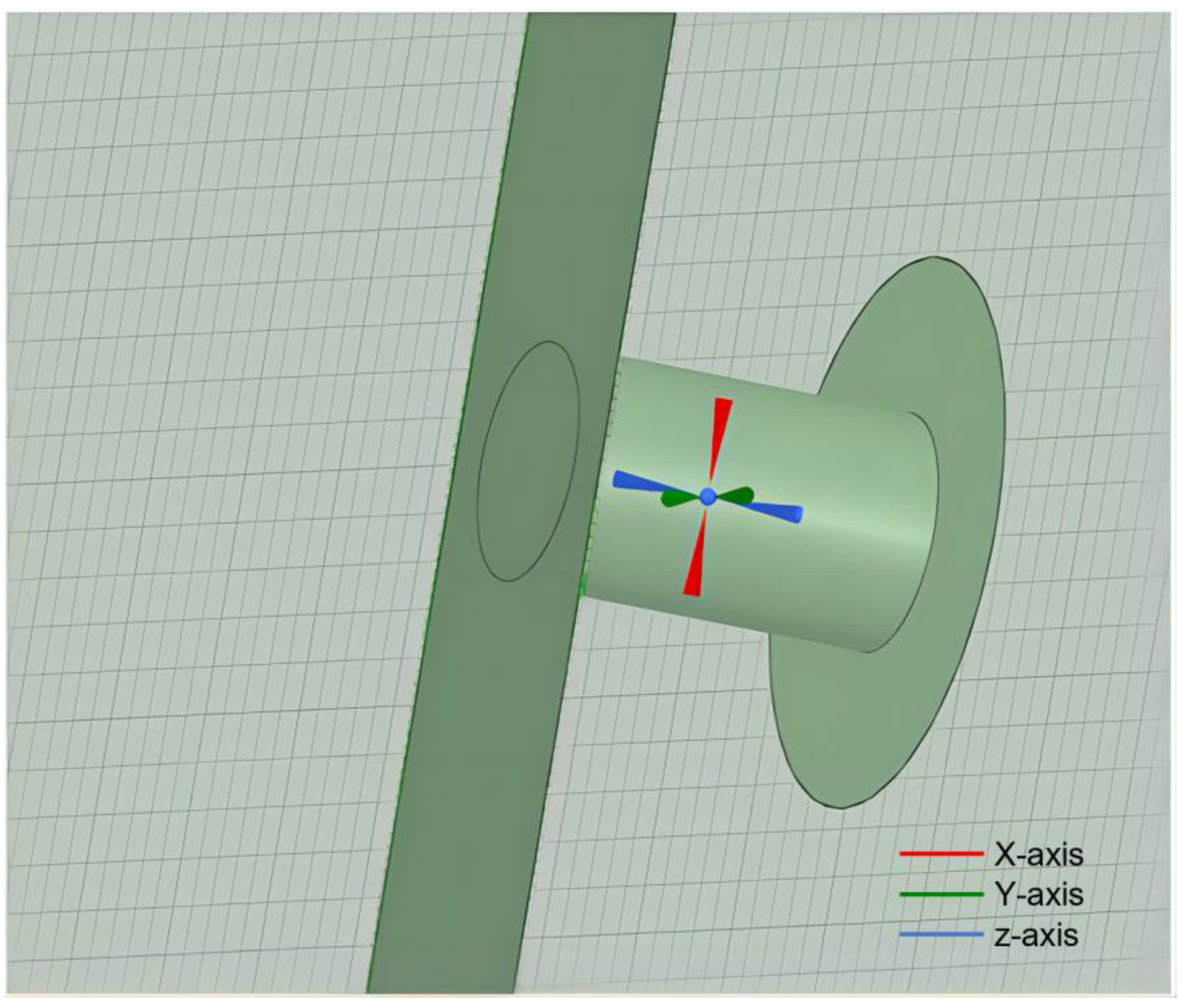
4.2.1. Design and Simulation of the Loop Antenna
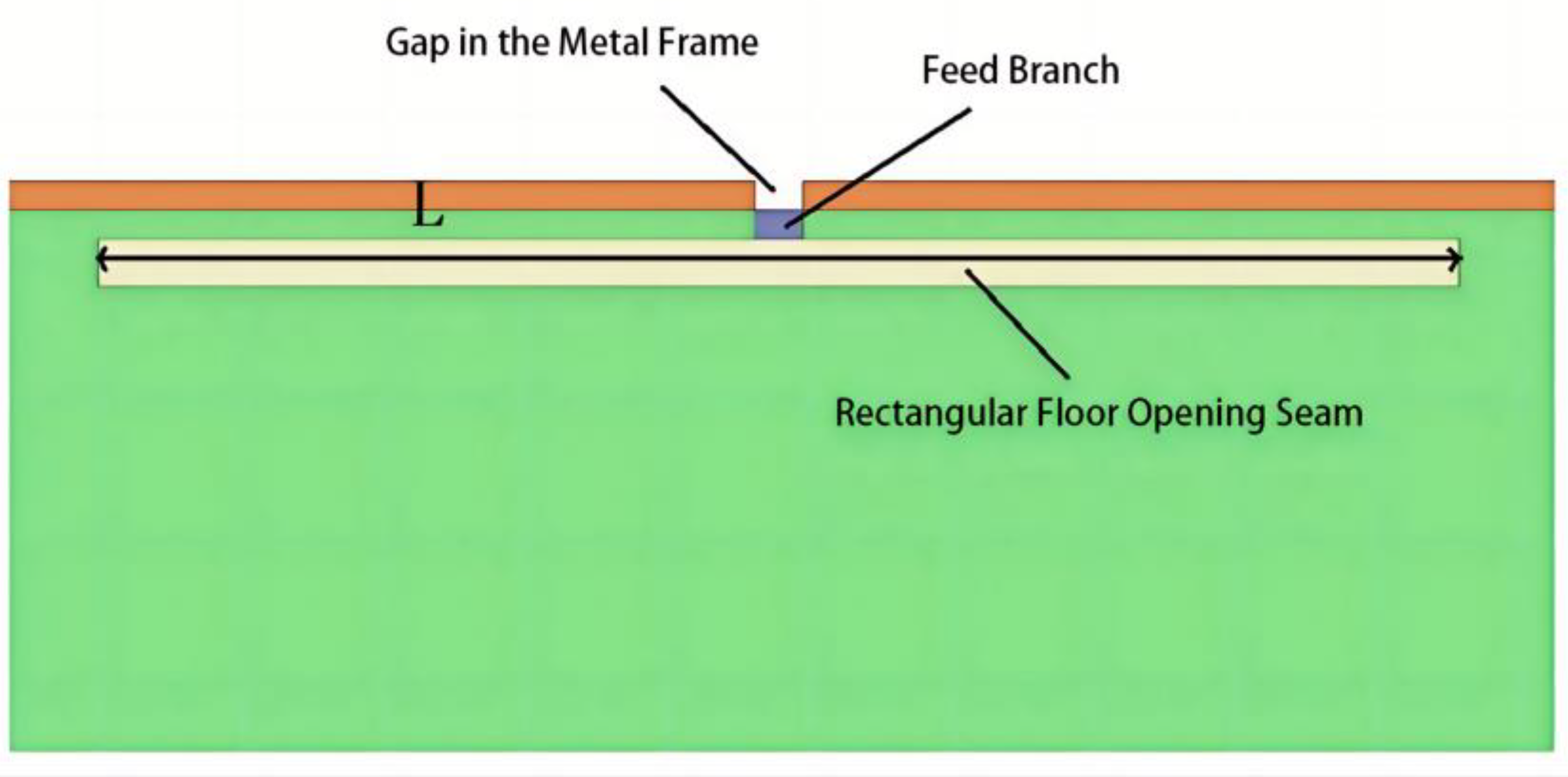
4.2.2. Design and Simulation of the Slot Antenna
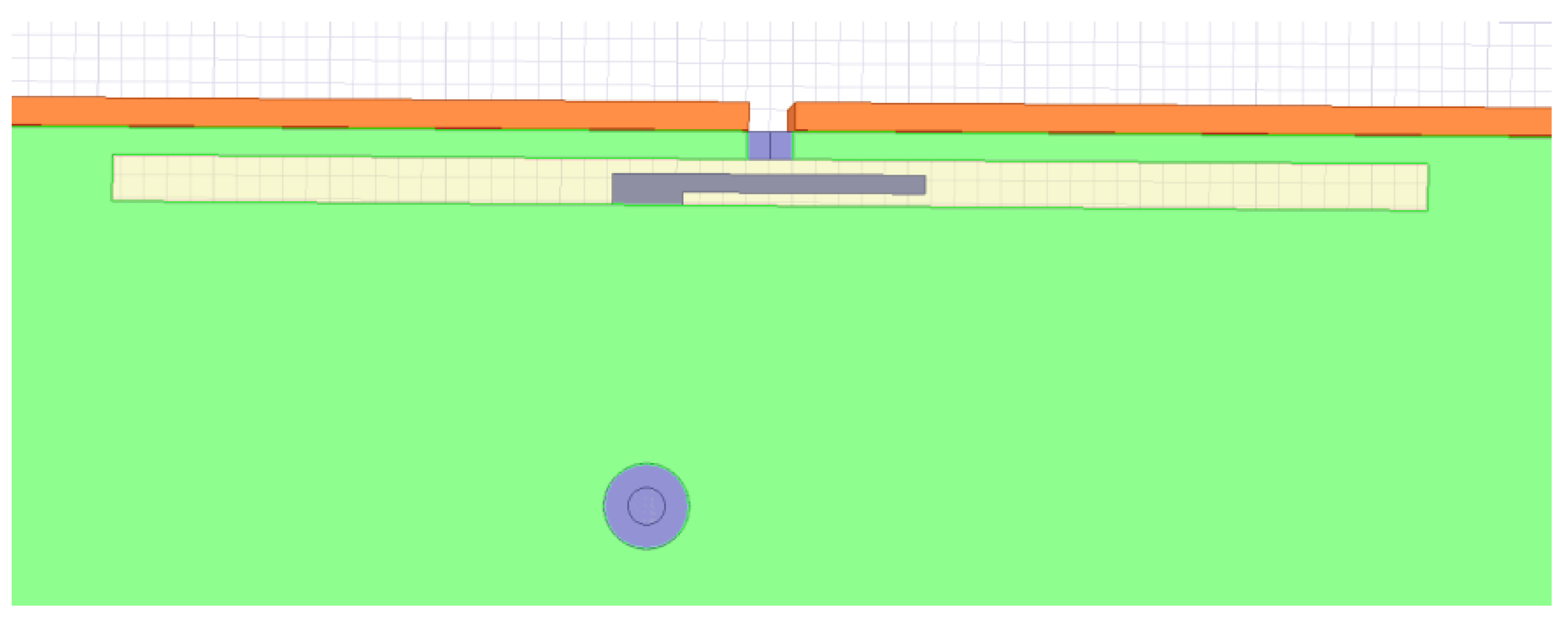
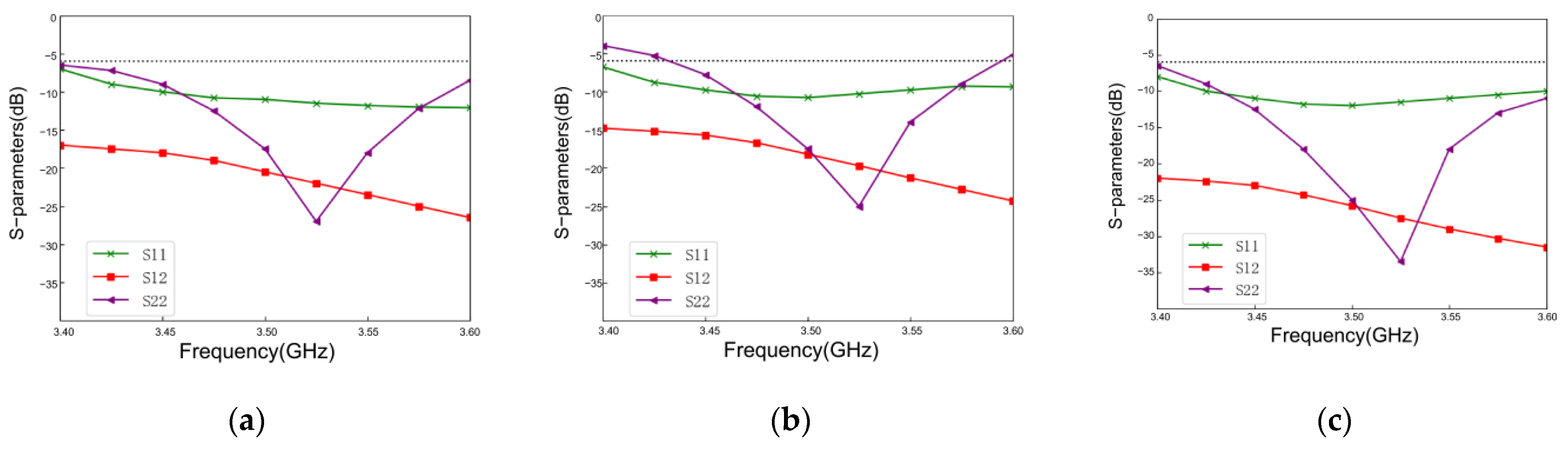
4.2.3. Implementation of a Dual-Element “Ring Slot” MIMO Antenna
4.3. Optimization of the “Ring-Slot” Structure Parameters
4.3.1. Optimization of Metal Frame Height
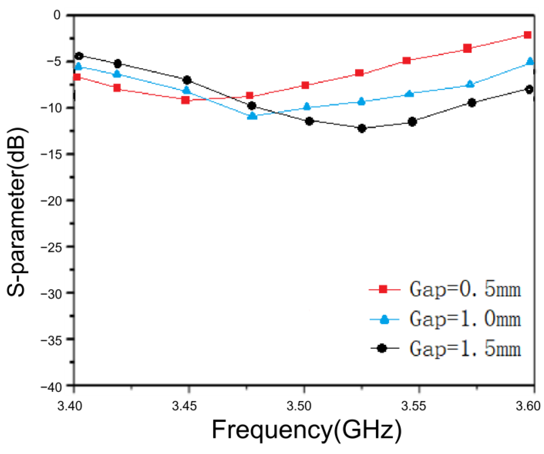
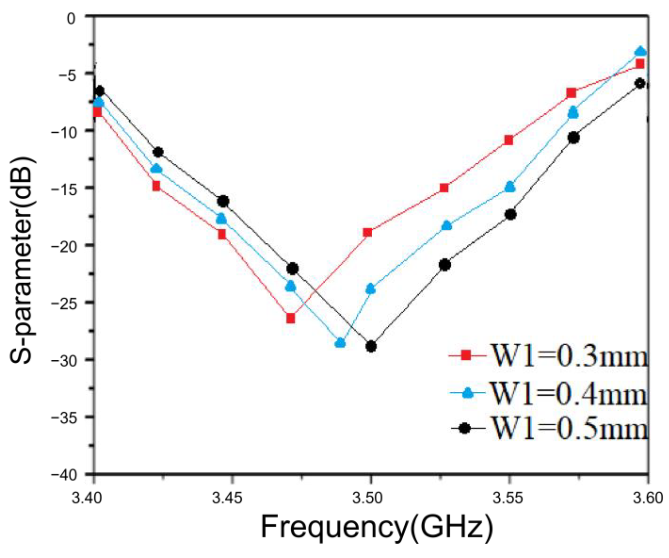
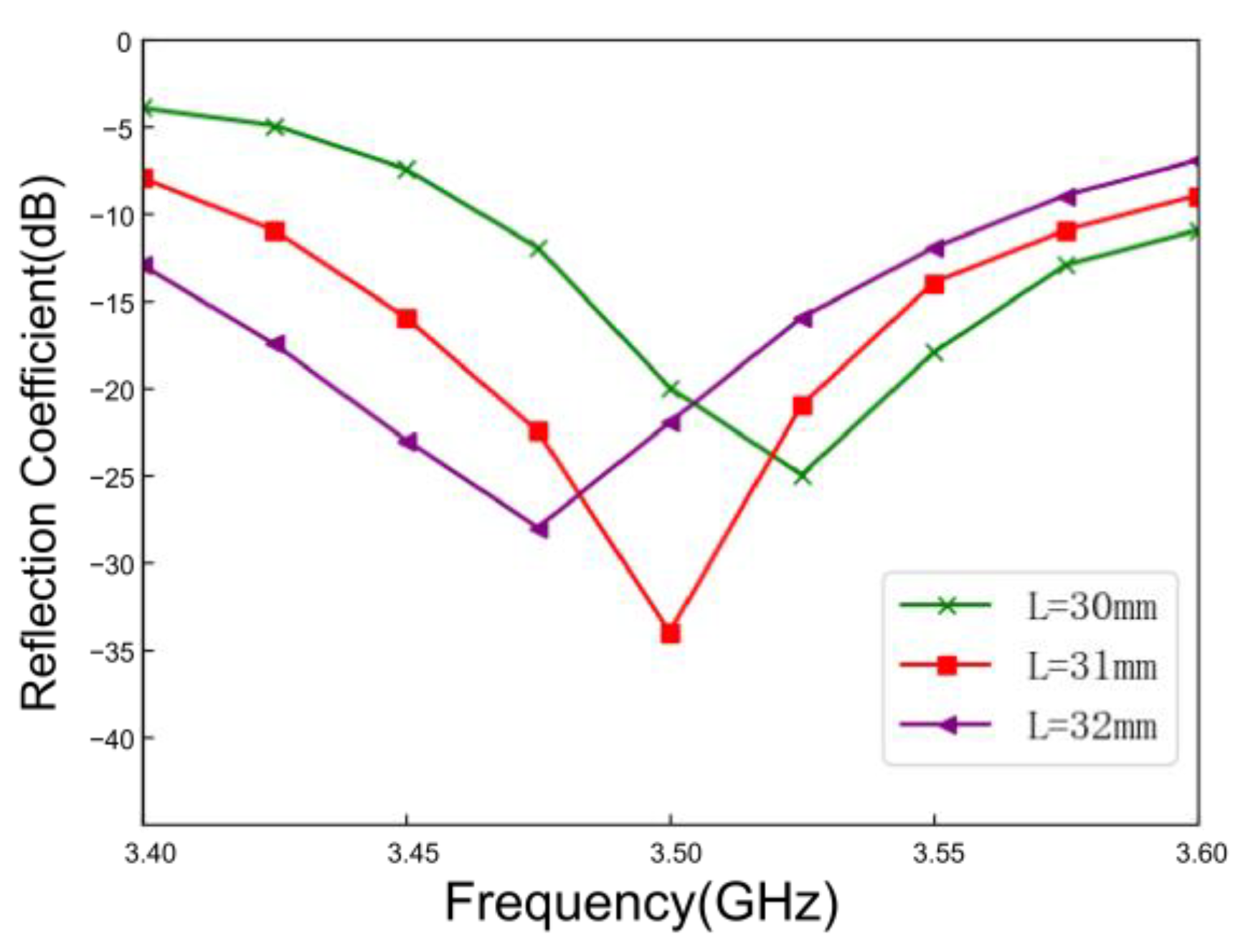
4.3.2. Optimization of Ground Slot Length
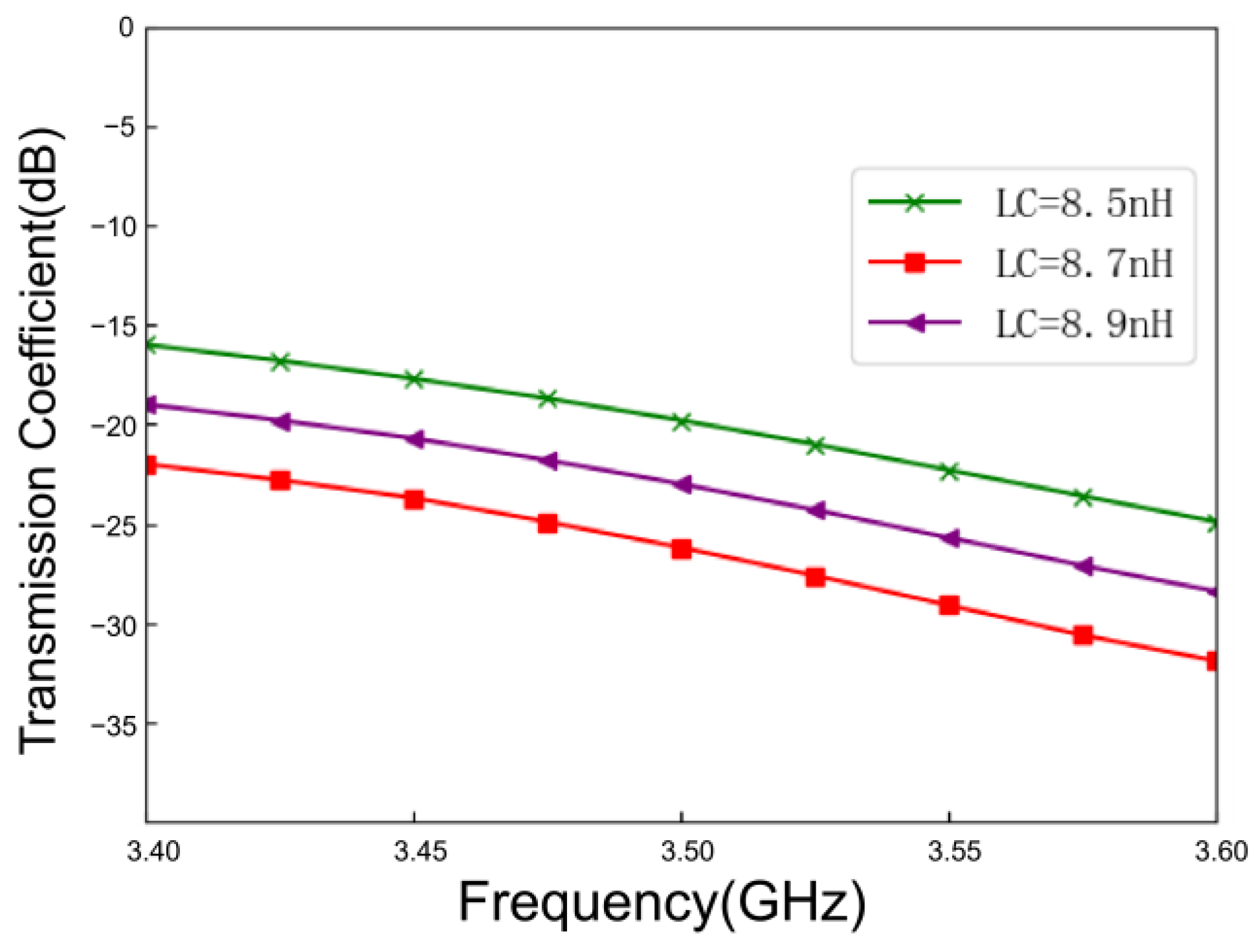
4.3.3. Optimization of the Chip Inductor
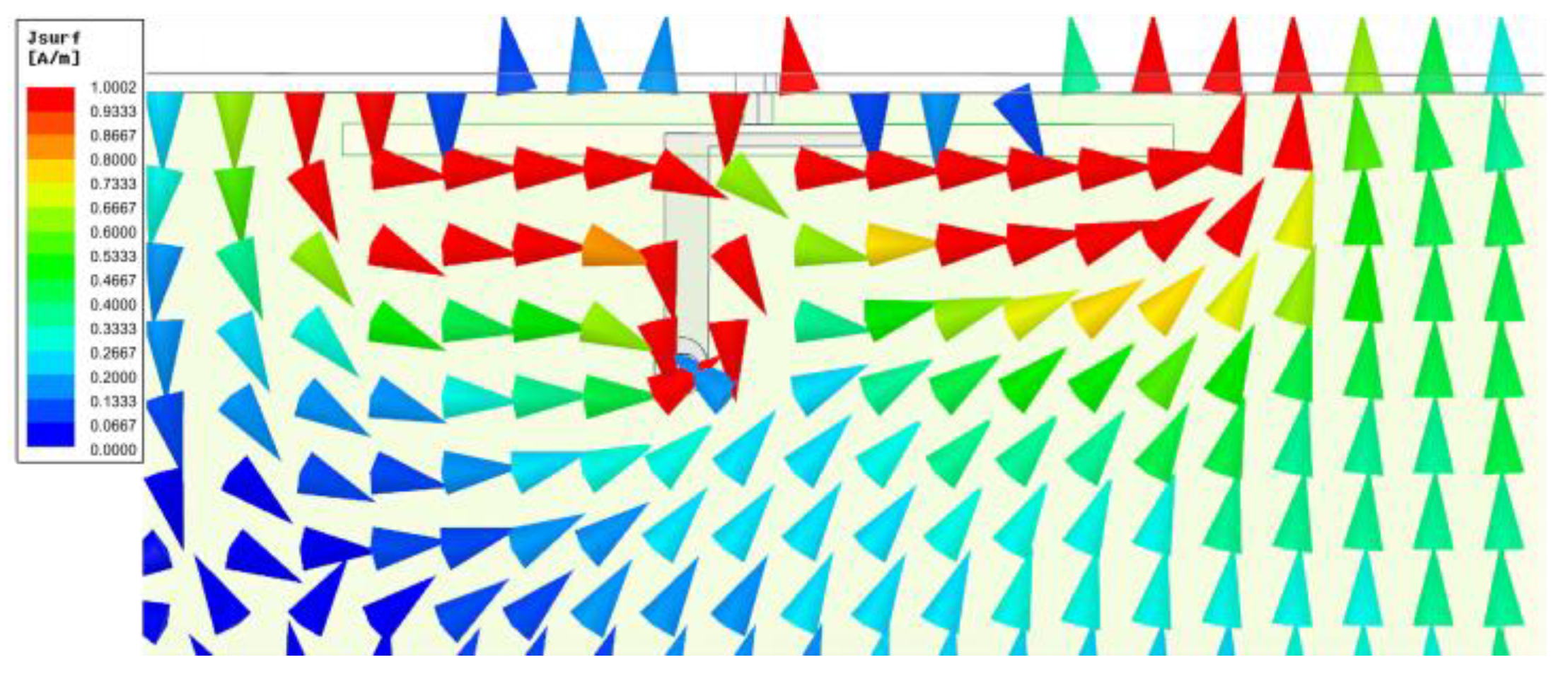
4.4. The Decoupling Principle of the “Ring-Slot” Structure
- Both antenna elements excite completely different resonant modes. When this occurs, an analysis of the overall structure is needed to find the most suitable placement for the antenna elements. However, this approach has limitations in practical antenna design.
- Both antenna elements can excite partially similar or completely identical resonant modes. In this section, for a mobile terminal antenna with added metal frame, operating in the 3.4–3.6 GHz frequency range, the ring antenna element and the slot antenna element can excite multiple identical resonant modes. In a dual-element “ring-slot” MIMO antenna system, the radiated electric fields from the ring antenna and slot antenna can be represented as a superposition of characteristic electric fields.
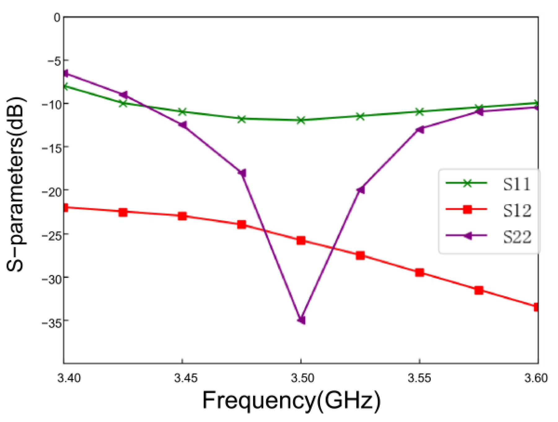
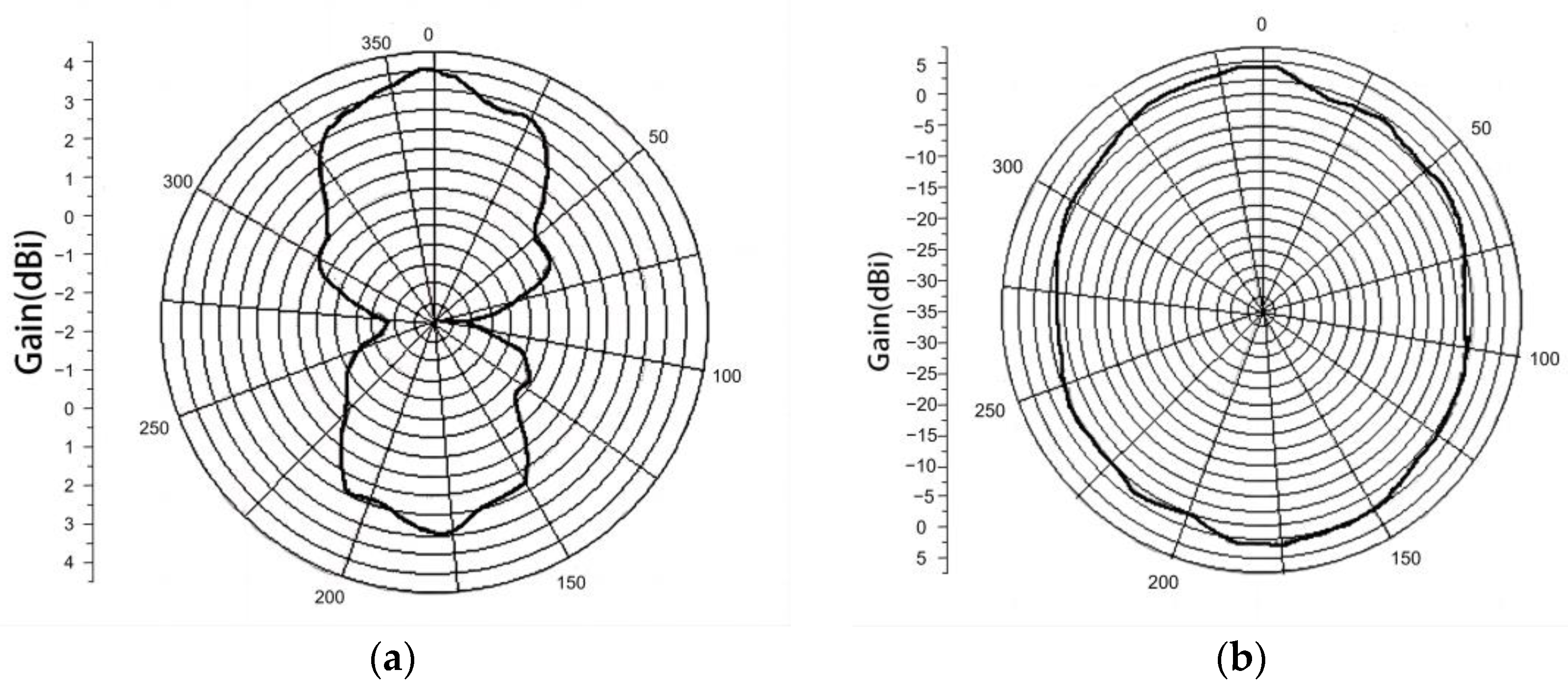
4.5. Results Analysis
5. Design of an Eight-Element MIMO Array Antenna for Mobile Terminals with a Metal Frame
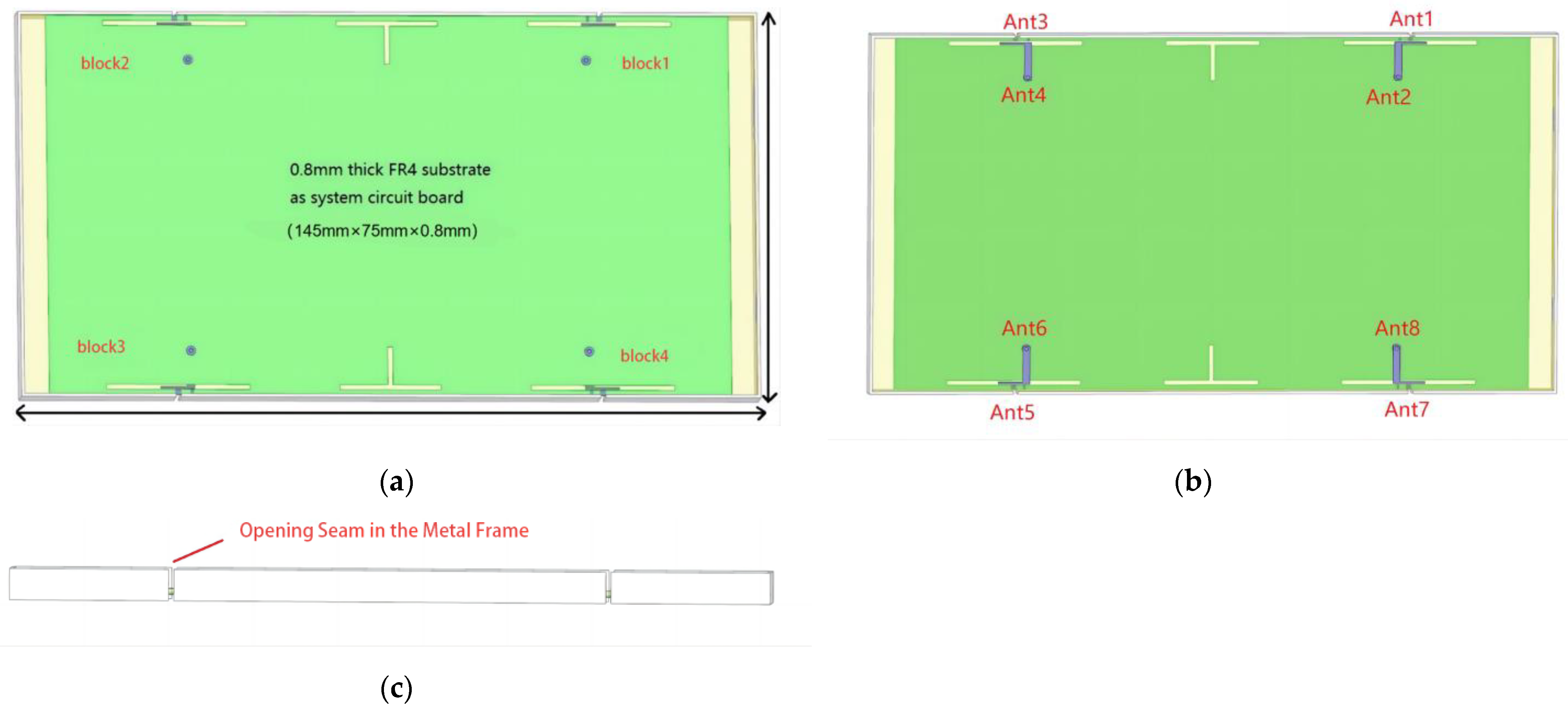
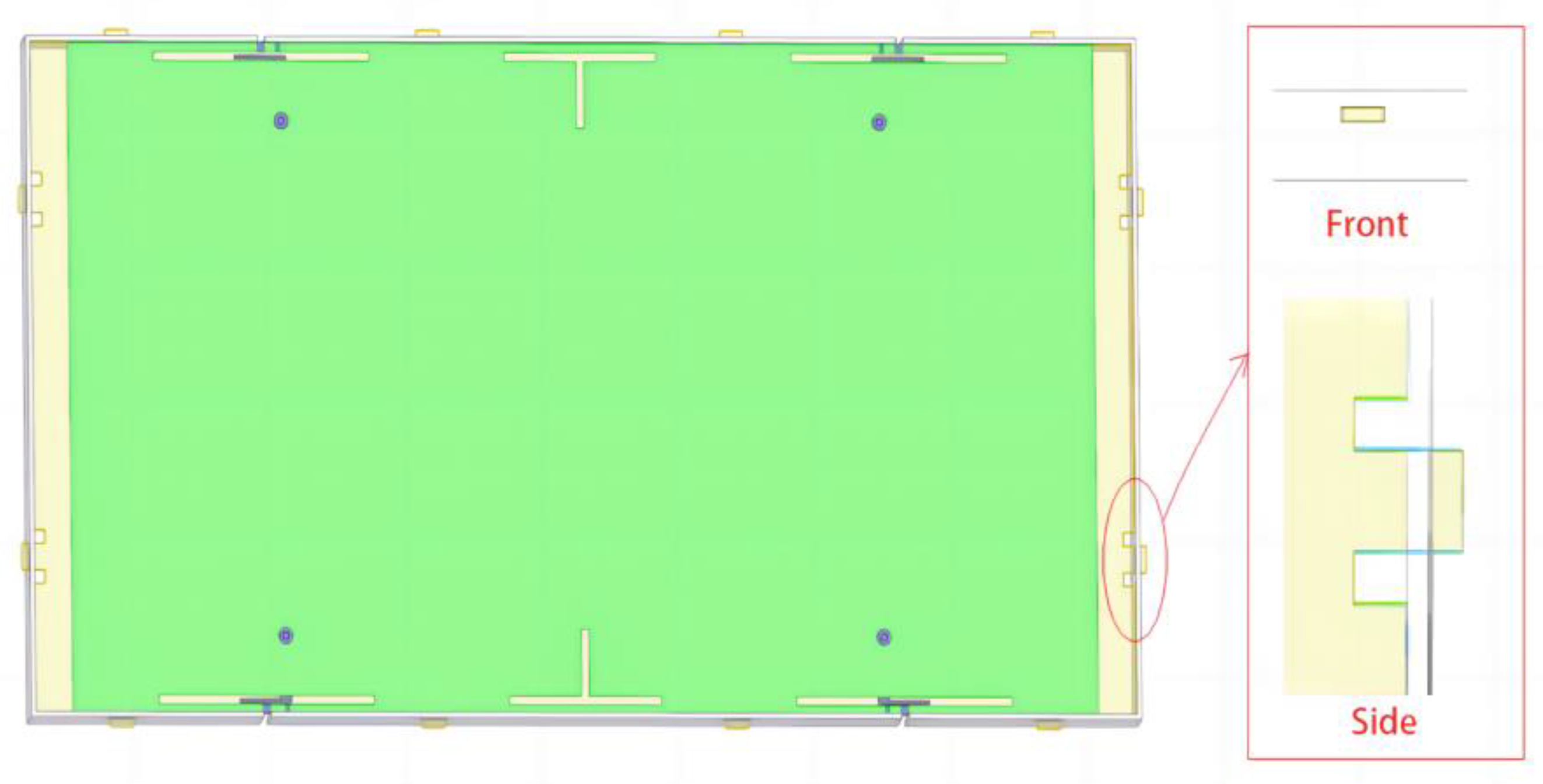
5.1. Design and Simulation of an Eight-Element MIMO Array Antenna
5.2. Optimization of the Parameters for the Eight-Element MIMO Array Antenna
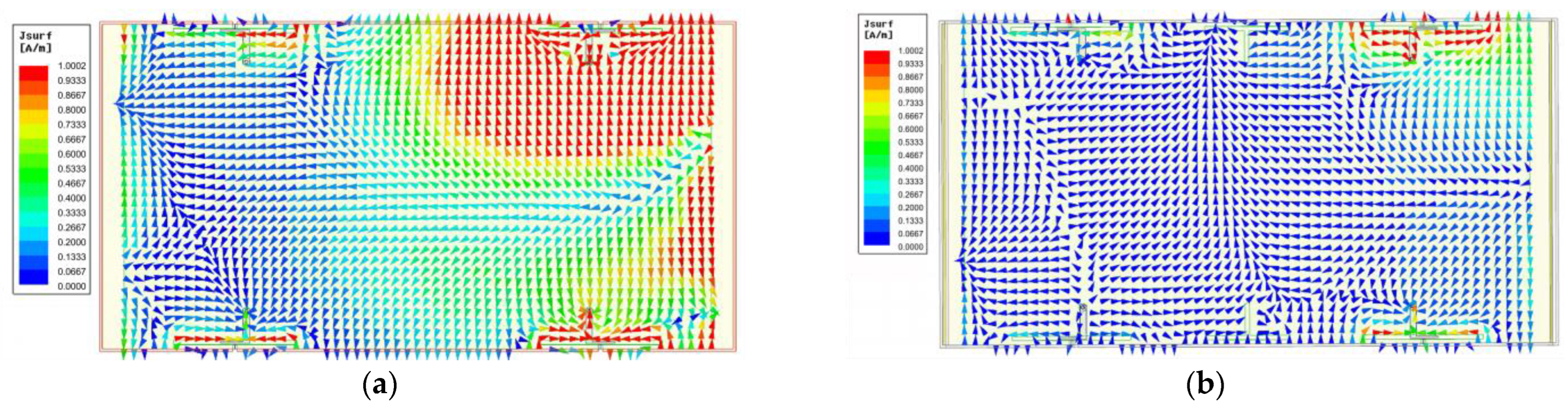
5.2.1. Adding T-Type Decoupling Structures
5.2.2. Layout of the “Ring-Slot” Unit Modules
5.2.3. Optimization of the Spacing between the “Ring-Slot” Unit Modules
5.3. Fabrication and Measurement of the Eight-Element MIMO Array Antenna
5.3.1. Fabrication of the Antenna
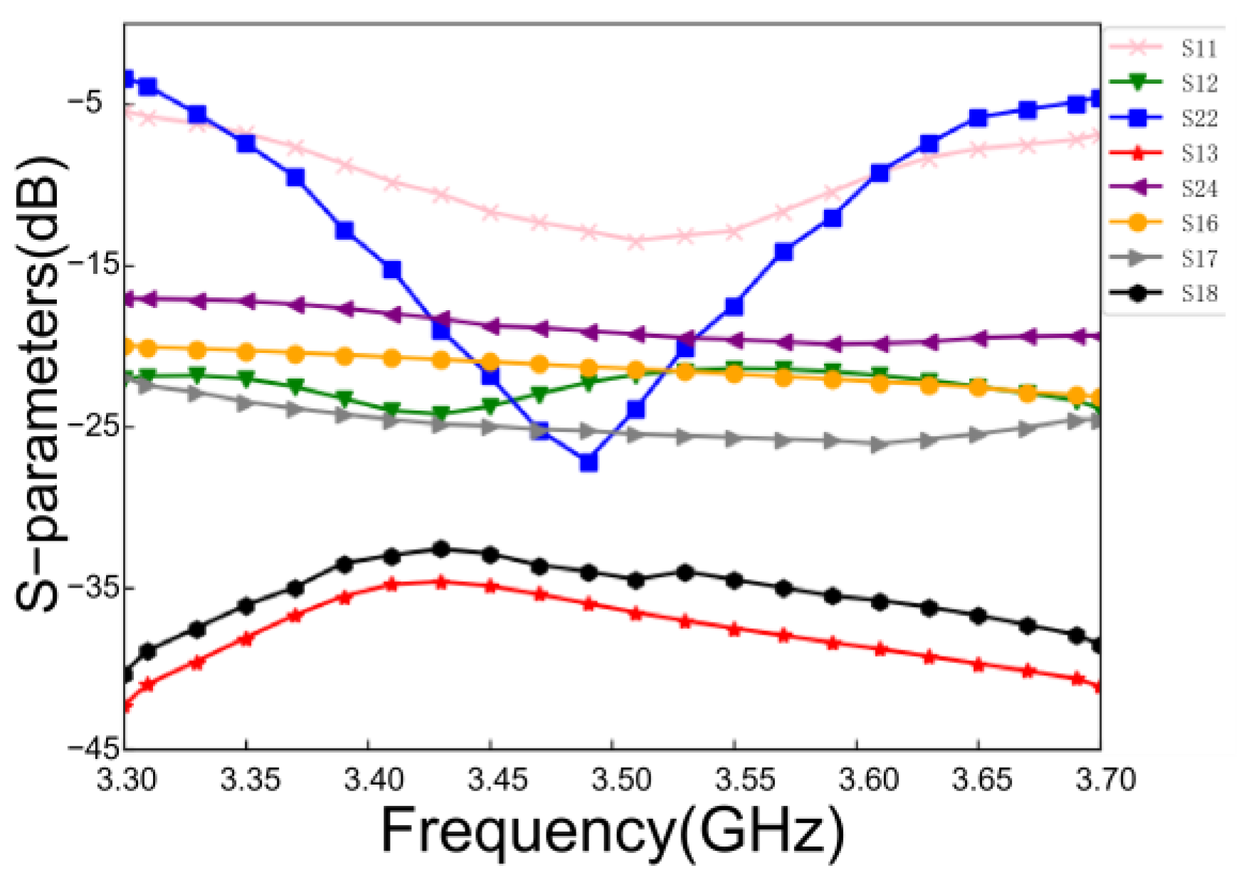
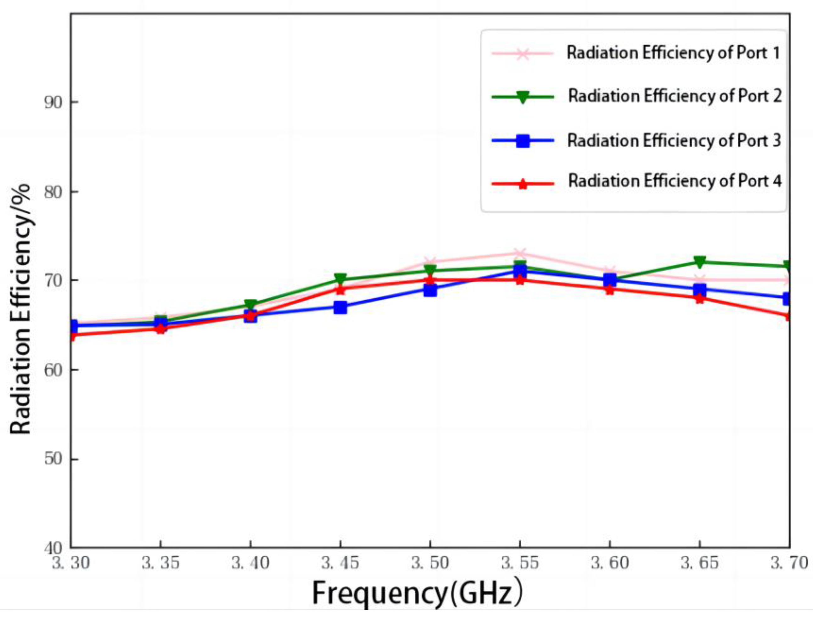
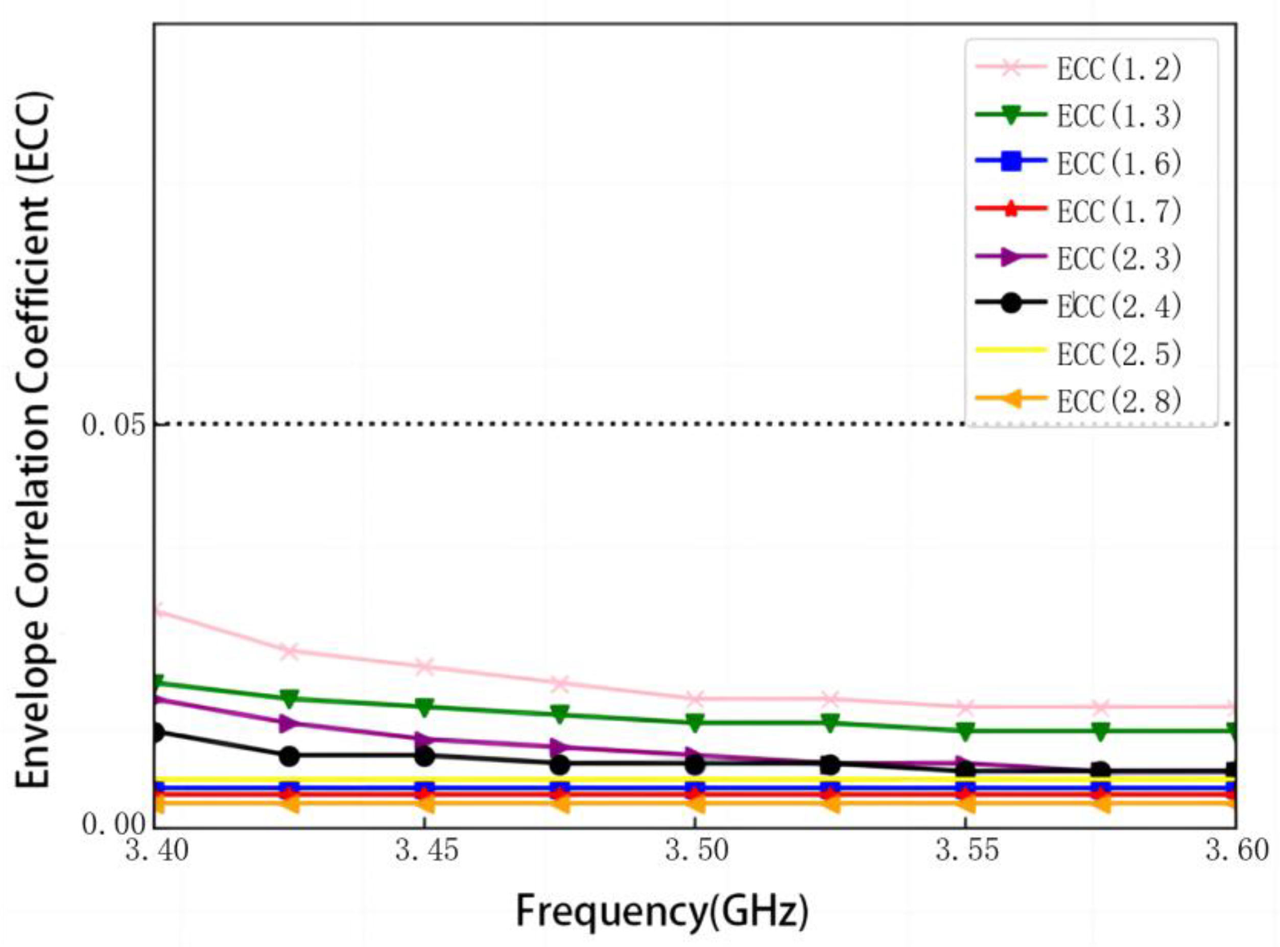
5.3.2. Analysis of Antenna Performance Results
6. Conclusions and Future Outlook
Author Contributions
Funding
Institutional Review Board Statement
Informed Consent Statement
Data Availability Statement
Conflicts of Interest
References
- Zhuhui, Y. Research and Design of High Performance Broadband Dual Polarization Microstrip Patch Antenna. Master’s Thesis, Xi’an University of Science and Technology, Xi’an, China, 2020. [Google Scholar]
- Fengyi, Y.; Weiliang, X.; Jianming, Z. 5G Wireless Network and Key Technologies, 1st ed.Posts & Telecom. Press: Beijing, China, 2017; p. 391. [Google Scholar]
- Di, X. Research on Hybrid Precoding Algorithm of Millimeter Wave Massive MIMO System. Master’s Thesis, Xidian University, Xi’an, China, 2020. [Google Scholar]
- Long, L.F. Research and Design of MIMO Antenna. Master’s Thesis, Xidian University, Xi’an, China, 2020. [Google Scholar]
- Tan, Z.-Y.; Li, P.-H. Comparative Discussion of Millimeter Wave Microstrip Antenna based on Multiple Feeding Methods. Commun. Technol. 2020, 53, 2136–2141. [Google Scholar]
- Hui-Qing, C.; Yu-Feng, P.; Xue-Yun, H.; Yi, Z. The Design of Microstrip Patch Antenna Based on Small Coaxial Feed. Tech. Autom. Appl. 2020, 39, 72–74. [Google Scholar]
- Xiaoyuan, Z.; Runbo, M.; Jiao, Z.; Yufeng, L. Design of Dielectric Rod Antenna Based on Microstrip Feeding. J. Test Meas. Technol. 2020, 34, 89–92. [Google Scholar]
- Chunchao, X.; Min, D. Study on the Design of Microstrip Array Antenna for Microdeformation Radar. Technol. Highw. Transp. 2020, 36, 73–77. [Google Scholar]
- Nilsson, A.; Bodlund, P.; Stjernman, A.; Johansson, M.; Derneryd, A. Compensation Network for Optimizing Antenna System for MIMO Application, Proceedings of the 2nd European Conference on Antennas and Propagation, EuCAP 2007, Edinburgh, UK, 11–16 November 2007; Institution of Engineering and Technology: Edinburgh, UK, 2007. [Google Scholar]
- Lu, J.-Y.; Wong, K.-L.; Li, W.-Y. Compact eight-antenna array in the smartphone for the 3.5GHz LTE 8×8 MIMO operation. IEEE Asia-Pac. Conf. Antennas Propag. 2016, 22, 323–324. [Google Scholar]
- Wong, K.L.; Li, Y.J. Low-Profile Open-Slot Antenna with Three Branch Slots for Triple-Wideband Lte Operation in the Metal-Framed Smartphone. Microw. Opt. Technol. Lett. 2015, 10, 2231–2238. [Google Scholar] [CrossRef]
- Huang, D.W.; Du, Z.W. Eight-Band Antenna with A Small Ground Clearance for LTE Metal-Frame Mobile Phone Applications. IEEE Antennas Wirel. Propag. Lett. 2018, 17, 34–37. [Google Scholar] [CrossRef]
- Li, M.Y.; Ban, Y.L.; Xu, Z.Q.; Guo, J.H.; Yu, Z.F. Tri-Polarized 12-Antenna MIMO Array for Future 5G Smartphone Applications. IEEE Access 2018, 6, 6160–6170. [Google Scholar] [CrossRef]
- Yueru, L. Design of the New Miniaturized Broadband Bow-Tie Antenn. Master’s Thesis, Southwest Jiaotong University, Chengdu, China, 2020. [Google Scholar]
- Zesheng, Z. Research on Compact Wideband Magneto-Electric Dipole Antenna. Master’s Thesis, Hangzhou Dianzi University, Hangzhou, China, 2019. [Google Scholar]
- Ritu, W. Design Of Phaesd Array Antenna Applied to 5g Frequency Ban. Master’s Thesis, Inner Mongolia University, Hohhot, China, 2021. [Google Scholar]
- Lu, L. Research on Some Key Technologies of Wideband Array Transmitting Antenna. Ph.D. Thesis, Xidian University,, Xi’an, China, 2020. [Google Scholar]
- Liang, Q. Research on Array antenna synthesis algorithm and its application. Master’s Thesis, China West Normal University, Nanchong, China, 2021. [Google Scholar]
- Zhang, L. MIMO Antenna for Terminal under Metal Boundary. Master’s Thesis, University of Electronic Science and Technology of China, Chengdu, China, 2018. [Google Scholar]
- Jia, Y. Design of Miniaturized 5G Communication Filter and Antenna Based on LTCC. Master’s Thesis, China University of Mining and Technology, Xuzhou, China, 2020. [Google Scholar]
- Wen-Tao, Z. Design of a Series-Fed Microstrip Plane Array Antenna. Electron. Qual. 2020, 9, 91–94. [Google Scholar]
- Su-Wei, C.; Chueh-Jen, L.; Wen-Tsai, T.; Tzu-Chieh, H.; Po-Chia, H. Design of Millimeter-Wave Antenna-in-Package (AiP) for 5G NR. ZTE Commun. 2020, 18, 26–32. [Google Scholar]
- Chengwen, Z.; Feihuang, C. Influencing Factors of Mutual Coupling Effect of Antenna Array. Instrum.·Anal.·Monit. 2017, 1, 21–25. [Google Scholar]
- Zijian, Z. Optimal Design of Several Typical Antenna Array. Master’s Thesis, Nanjing University of Information Science & Technology, Nanjing, China, 2017. [Google Scholar]
- Li, R. 5G Technology Induced Application of Indoor Antenna with Advanced Devices. Master’s Thesis, University of Electronic Science and Technology of China, Chengdu, China, 2021. [Google Scholar]
- Zhou, Q.-Q. Common-Metal-Frame MIMO Antenna for Terminal Device. Master’s Thesis, University of Electronic Science and Technology of China, Chengdu, China, 2017. [Google Scholar]
- Wang, W. Research on Multi-band High-isolation Antenna. Master’s Thesis, Beijing University of Posts and Telecommunications, Beijing, China, 2021. [Google Scholar]
- Zeng, W. Research on Wireless Channel Modeling and Channel State Information Acquisition of Massive MIMO Systems. Ph.D. Thesis, Hefei University of Technology, Hefei, China, 2021. [Google Scholar]
- Gaoya, J.; Chengzhu, D.; Zhejing, J.; Fuhui, Y. A high isolation triple band-notched ultra-wideband multiple-input-multiple-output antenna. Electron. Compon. Mater. 2021, 40, 93–98. [Google Scholar]


| Parameters | Value | Units |
|---|---|---|
| ) | 3.5 | GHz |
| Relative dielectric constant (εᵣ) | 4.4 | \ |
| Substrate thickness (h) | 1.6 | mm |
| Patch width (W) | 22 | mm |
| Effective dielectric constant (εe) | 3.99 | \ |
| Equivalent radiating aperture length (ΔL) | 0.734 | mm |
| Patch length (L) | 19.6 | mm |
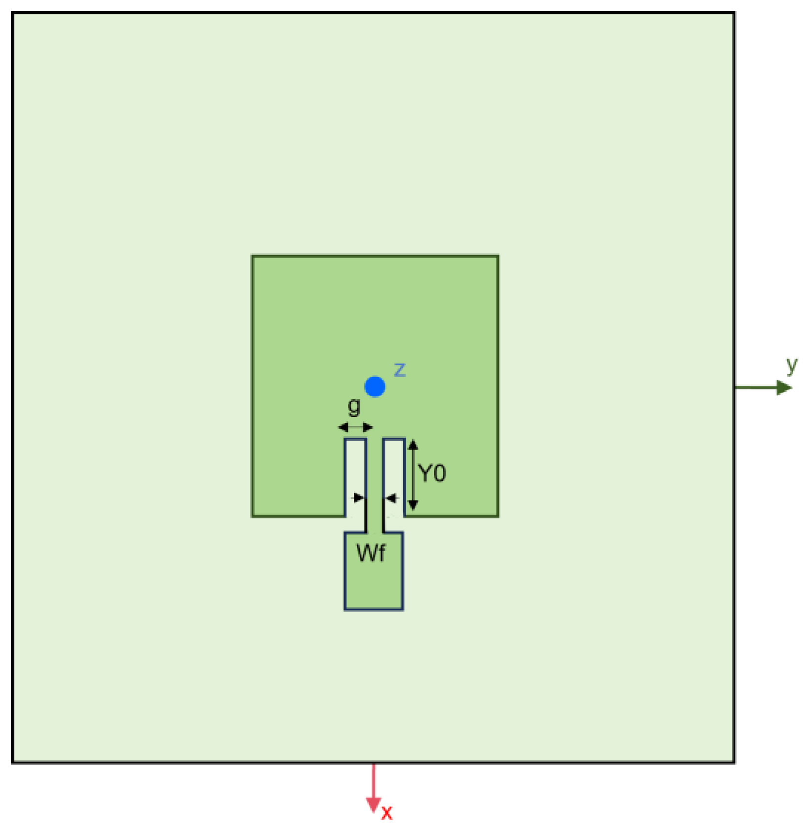
| Parameters | Values (mm) |
|---|---|
| Microstrip feedline width (Wf) | 1 |
| Embedding depth (Y0) | 5.25 |
| Embedding width (g) | 1.5 |
Disclaimer/Publisher’s Note: The statements, opinions and data contained in all publications are solely those of the individual author(s) and contributor(s) and not of MDPI and/or the editor(s). MDPI and/or the editor(s) disclaim responsibility for any injury to people or property resulting from any ideas, methods, instructions or products referred to in the content. |
© 2024 by the authors. Licensee MDPI, Basel, Switzerland. This article is an open access article distributed under the terms and conditions of the Creative Commons Attribution (CC BY) license (https://creativecommons.org/licenses/by/4.0/).
Share and Cite
Li, K.; Wu, D.; Chu, D.; Ping, L. Simulation and Design of Three 5G Antennas. Appl. Sci. 2024, 14, 8032. https://doi.org/10.3390/app14178032
Li K, Wu D, Chu D, Ping L. Simulation and Design of Three 5G Antennas. Applied Sciences. 2024; 14(17):8032. https://doi.org/10.3390/app14178032
Chicago/Turabian StyleLi, Keyu, Dongsheng Wu, Dapeng Chu, and Lanlan Ping. 2024. "Simulation and Design of Three 5G Antennas" Applied Sciences 14, no. 17: 8032. https://doi.org/10.3390/app14178032
APA StyleLi, K., Wu, D., Chu, D., & Ping, L. (2024). Simulation and Design of Three 5G Antennas. Applied Sciences, 14(17), 8032. https://doi.org/10.3390/app14178032