Article

Multi-Layer QCA Reversible Full Adder-Subtractor Using Reversible Gates for Reliable Information Transfer and Minimal Power Dissipation on Universal Quantum Computer

Department of Convergence Science, Kongju National University, Gongju 32588, Republic of Korea
Appl. Sci. 2024, 14(19), 8886; https://doi.org/10.3390/app14198886
Submission received: 16 August 2024 / Revised: 1 September 2024 / Accepted: 30 September 2024 / Published: 2 October 2024

Abstract

:
The effects of quantum mechanics dominate nanoscale devices, where Moore’s law no longer holds true. Additionally, with the recent rapid development of quantum computers, the development of reversible gates to overcome the problems of energy and information loss and the nano-level quantum-dot cellular automata (QCA) technology to efficiently implement them are in the spotlight. In this study, a full adder-subtractor, a core operation of the arithmetic and logic unit (ALU), the most important hardware device in computer operations, is implemented as a circuit capable of reversible operation using QCA-based reversible gates. The proposed circuit consists of one reversible QCA gate and two Feynman gates and is designed as a multi-layer structure for efficient use of area and minimization of delay. The proposed circuit is tested on QCADesigner 2.0.3 and QCADesigner-E 2.2 and shows the best performance and lowest energy dissipation. In particular, it shows tremendous improvement rates of 180% and 562% in two representative standard design cost indicators compared to the best existing studies, and also shows the highest circuit average output polarization.

1. Introduction

The International Technology and Roadmap for Semiconductors (ITRS) points out major problems with existing CMOS technology, such as high-power loss, threshold voltages, thermal runaway, and high leakage current, and states that it is approaching the end of its semiconductor nano-system roadmap [1]. Moore’s law, which states that the number of components on a single chip doubles approximately every two years [2], no longer applies in nanoscale devices, and various quantum mechanical effects dominate device physics [3]. In addition, as CMOS-VLSI micro technology reduces the size of transistors disproportionately, large energy and information losses are emerging as major problems. Information loss is a major problem in irreversible digital computation systems, and there is a large and growing demand for nanoscale computation systems that can minimize heat dissipation [4].
Therefore, the design of reversible circuits is a key structural engineering challenge for solving the problem of information loss while minimizing energy dissipation. Landauer demonstrated that 1-bit information loss results in energy dissipation of kBTln2 joules, where kB = 1.38 × 10⁻²³ JK−1 is the Boltzmann constant and T is the temperature in Kelvin [5]. At room temperature (T = 300 K), the heat release occurring during a binary transaction is 0.017 eV and is considered physically irreversible, and this microscopic physical state can be restored to what it was before the process occurred. Bennett demonstrated the validity that energy loss of kBTln2 joules in an irreversible circuit can be recovered in a reversible circuit [6].
Recently, with the rapid rise of quantum computing [7], quantum logic gates are attracting attention as logic gates that can replace existing digital circuits in quantum circuit calculation models. The Toffoli gate, developed in 1980, is a universal gate that can implement any desired Boolean function as a reversible circuit [8], and it can be realized by five two-qubit quantum gates [9]. Along with this, various universal reversible gates, such as the Fredkin gate, Feynman gate, and Peres, were developed [10,11,12]. Since then, various reversible gates, such as RUG [13], RQCA [14], URG [15], TR [16], and PQR [17], have been continuously developed and implemented using QCA [18].
Quantum-dot cellular automata (QCA), proposed by Lent and Tougaw, has emerged as an alternative to overcome the problems of existing CMOS and implements existing reversible circuits with ultra-low power consumption. The dissipated energy is measured based on the Hamiltonian matrix, using the HartreeFock approximation in relation to the Coulomb repulsion between QCA cells, as shown in (1) [19].
H = E k 2 i C i f i , j γ γ E k 2 i C i f i , j = E k 2 C j 1 + C j + 1 γ γ E k 2 C j 1 + C j + 1
where E k is the energy cost of two neighboring cells with opposite polarization, called kink energy, C i denotes the polarization of the i-th neighboring cell, and f i , j denotes the geometrical factor identifying the electrostatic interaction between cells i and j due to the geometrical distance. This kink energy is related to the energy cost of two cells with the opposite polarization. γ denotes the electron tunneling energy inside the cell, which is controlled by the clock. The nonadiabatic power estimation model was used to estimate the power loss or energy dissipation of the cell [20,21]. The expected value of the Hamiltonian at each time instant is given by
E = H = 2 Г · λ
where Г is the 3-D energy vector, and λ is the coherence vector. Based on (2), the equation for instantaneous power is given as (3).
P T o t a l = d E d t = 2 d Г d t · λ + 2 Г · d d t λ
The first term in (4) represents the power going in and out of the clock and inter-cell power flow, and the second term represents the power dissipated. By multiplying these two terms, the power dissipation at a specific time can be obtained.
P d i s s ( t ) = 2 Г ( t ) · d d t λ ( t )
Therefore, power dissipation can be summarized in terms of energy per clock cycle, as shown in (5).
P d i s s = E d i s s T c 2 T c Г + × Г + Г + tanh Г + k B T + Г Г tanh Г k B T
where T c is the clock period and Г + and Г are the Hamiltonian values before and after the transaction processing.
Multilayer structures are a design method that minimizes energy dissipation and are a field of QCA design that is being studied extensively. Although feasibility is lower and design cost is higher than that of a co-planar structure, a well-designed multi-layer structure plays a significant role in minimizing space, delay, and energy consumption, and is continuously being studied at various major universities and research institutes. In 2020, Song et al. [22] and Heikalabad et al. [23] proposed a QCA-based RAM and full adder using a multi-layer structure, respectively, and in 2021, Chu et al. proposed a 3-input XOR-based QCA BCD adder using a multi-layer structure [24]. In 2022, Perri et al. [25] and Das et al. [26] proposed a QCA multi-bit comparator and a 3:8 decoder using a multi-layer crossover, respectively.
In 2023 and 2024, Khan et al. presented various analyses of the latest trends and problems related to QCA design [27,28]. In particular, much research has been conducted based on QCA on the full adder-subtractor (FAS), the core circuit of the ALU, which consumes the most power in computer processors [29,30,31], and research on reversible FAS (RFAS) continues to minimize energy dissipation. Recently, various reversible gates have been implemented using QCA.
Kianpour et al. designed a Toffoli gate and a Fredkin gate using a rotated QCA cell and proposed RFAS based on a QR gate using these gates [32]. Hashemi et al. and Kumar et al. proposed RFA without a subtractor along with a new reversible gate using a QCA-based 3-input majority gate and a 5-input majority gate, respectively [33,34]. Taherkhani et al. proposed a more efficient RFAS using the newly proposed reversible QCA gate (RQG) and two Feynman gates (FGs) [35], and Ahmad et al. developed a new reversible gate (NRG) using QCA-based multiple gates and FG, and proposed NRG-based RFAS [36]. Vahabi efficiently redesigned various reversible gates using QCA and proposed RFAS with excellent performance using the existing RQG [37]. Table 1 summarizes the major contributions to the development of RFA(S).
In this study, we review previously proposed QCA-based RFAS circuits and propose the most efficient RFAS that improves the problems of the circuits using QCA. The contributions of this study are summarized as follows.
  • Review of the structure, operation, and characteristics of existing excellent QCA-based RFAS circuits
  • Design of a reversible quantum gate (RQG)-based RFAS after presenting the problems of implementing the existing QCA circuits
  • Best performance in all aspects compared with the existing circuits and significant improvements of at least 67% and 54% in delay and energy dissipation, respectively.
  • Remarkable improvements of 180% and 562% in two representative design costs, CostAD and CostED, respectively, compared to the best existing circuit
  • Noise-free and high and stable output polarization, especially a significant improvement of 3.8% in the average output polarization
  • Proposal of an efficient QCA-based RFAS that minimizes information loss and provides reliable information transmission through the best performance of the proposed reversible circuit
The structure of the paper is as follows. Section 2 explains the basic operation principle of QCA and reviews existing QCA reversible full adder-subtractors. Section 3 explains the operation and structure of the proposed reversible full adder-subtractor. Section 4 analyzes and compares the results through simulations. Section 5 concludes.

2. Related Works

In this section, we look at basic gate operations and clock states using QCA, and review existing reversible gates and RFAS circuits based on them. Various reversible gates are being developed to optimize RFAS, but there are still many shortcomings in areas, delays, energy dissipation, and output polarization.

2.1. QCA Gates and Clock Sates

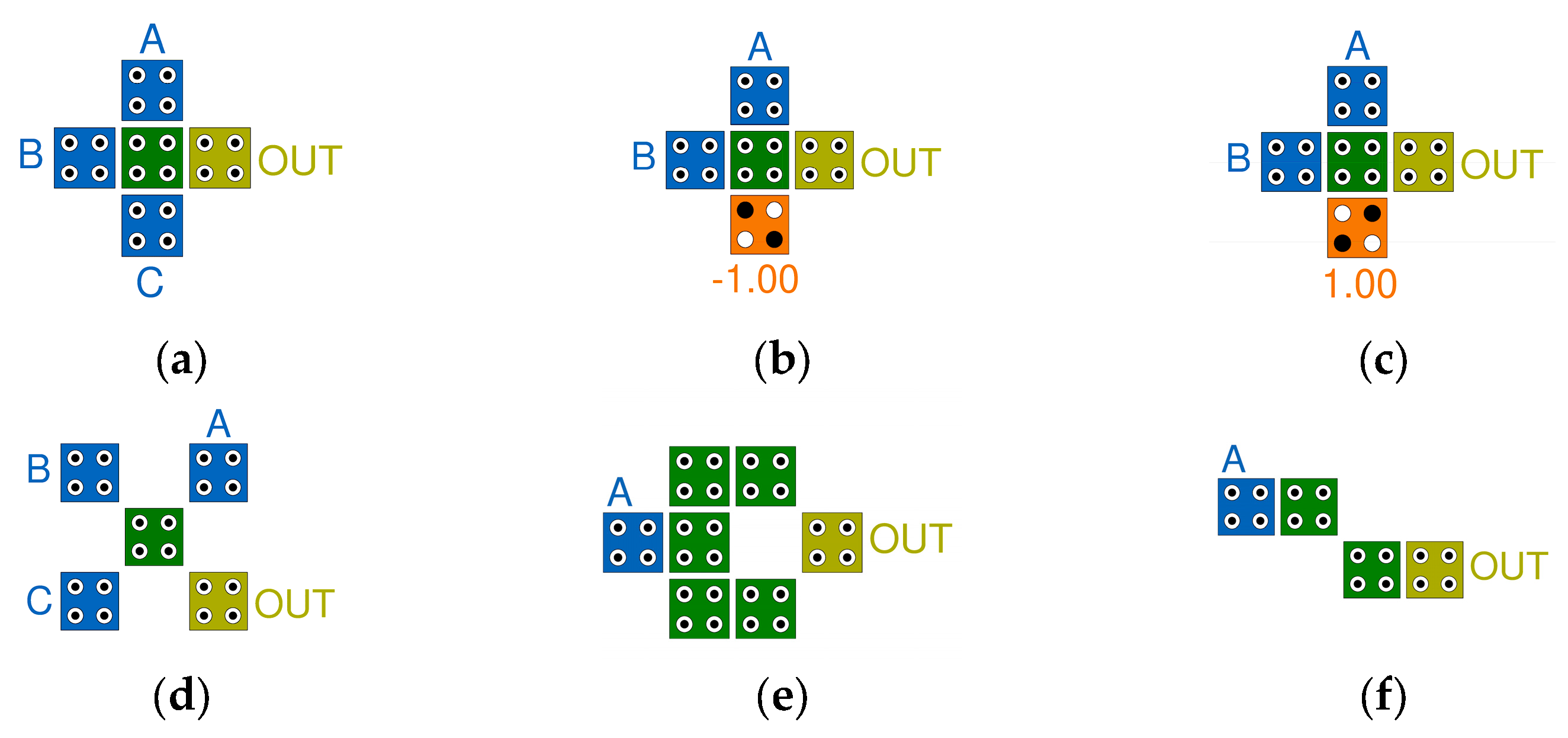
A QCA cell consists of four quantum dots and is located at each corner of a square. Two electrons repel each other by Coulomb repulsion and exist in two quantum dots located diagonally among the four quantum dots. There are two such cases, and each polarization is expressed as P = +1 or P = −1, and in binary operation, they correspond to “1” and “0”, respectively [38,39]. Logical operations in the QCA environment are based on a majority vote function in which the result value is the value of two or more of the three inputs and are implemented through a majority gate in the QCA environment. Figure 1a,d show a majority gate and a rotated majority gate with three inputs A, B, and C, respectively. If the polarization of one of these inputs is fixed to P = +1 or P = −1, it is used as a 2-input AND and OR logic gate, respectively, as shown in Figure 1b,c. Another representative logical operation is an Inverter. Figure 1e is a robust NOT gate that makes the output signal stronger, and Figure 1f is a simple NOT gate that can be easily implemented in a small space [40,41].
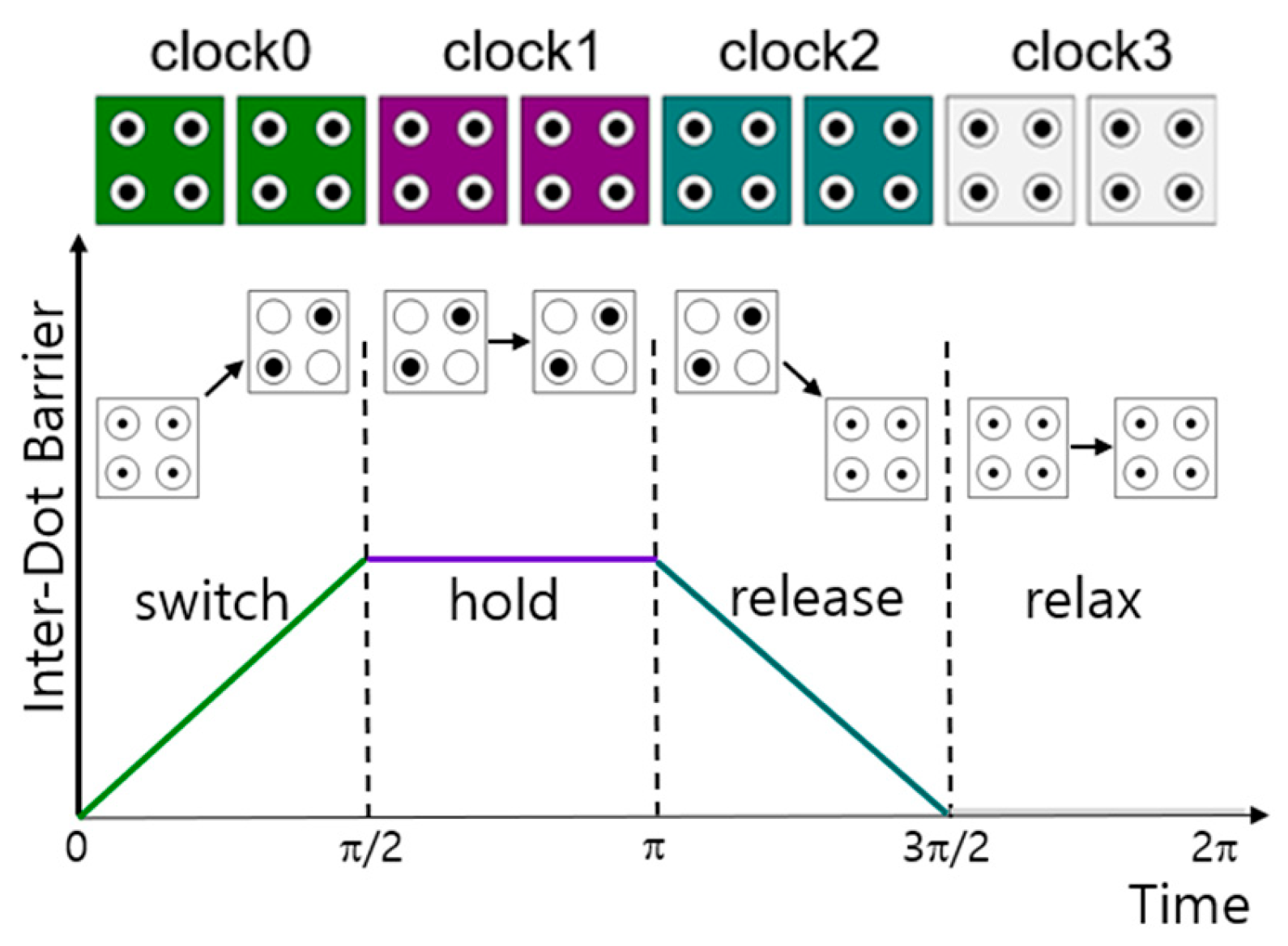
A QCA cell has four clock states, and the circuit operates by repeating changes from clock0 to clock3 [19,39]. The switch state refers to a state in which the barrier between quantum dots gradually increases as the potential energy of electrons becomes stronger. In the hold state, the potential energy of electrons becomes high enough to prevent them from crossing the barrier between quantum dots. At this time, each cell has a clear polarization and the strongest potential energy. In the release state, electrons gradually lose potential energy, and the barrier between quantum dots gradually decreases. In the relaxed state, the potential energy of the electrons is lowered so that they can freely pass through the barrier between quantum dots, and the cell does not have any polarization. Figure 2 shows a graph of the barrier height and time relationship between quantum dots according to the four states of the QCA cell.

2.2. Conventional QCA Reversible Full Adder-Subtractors

Recently, various reversible gates have been proposed, and efficient RFAS using them are being proposed. As shown in the truth table in Table 2, RFAS has three inputs, A, B, and C, and three outputs, Carry, Borrow, and Sum/Diff. It can also have additional garbage inputs and outputs to enable reversible operations. To obtain the output Carry, Borrow, and Sum/Diff, the operation of M G ( A , B , C ) , M G ( A , B , C ) , and A B C were used respectively.
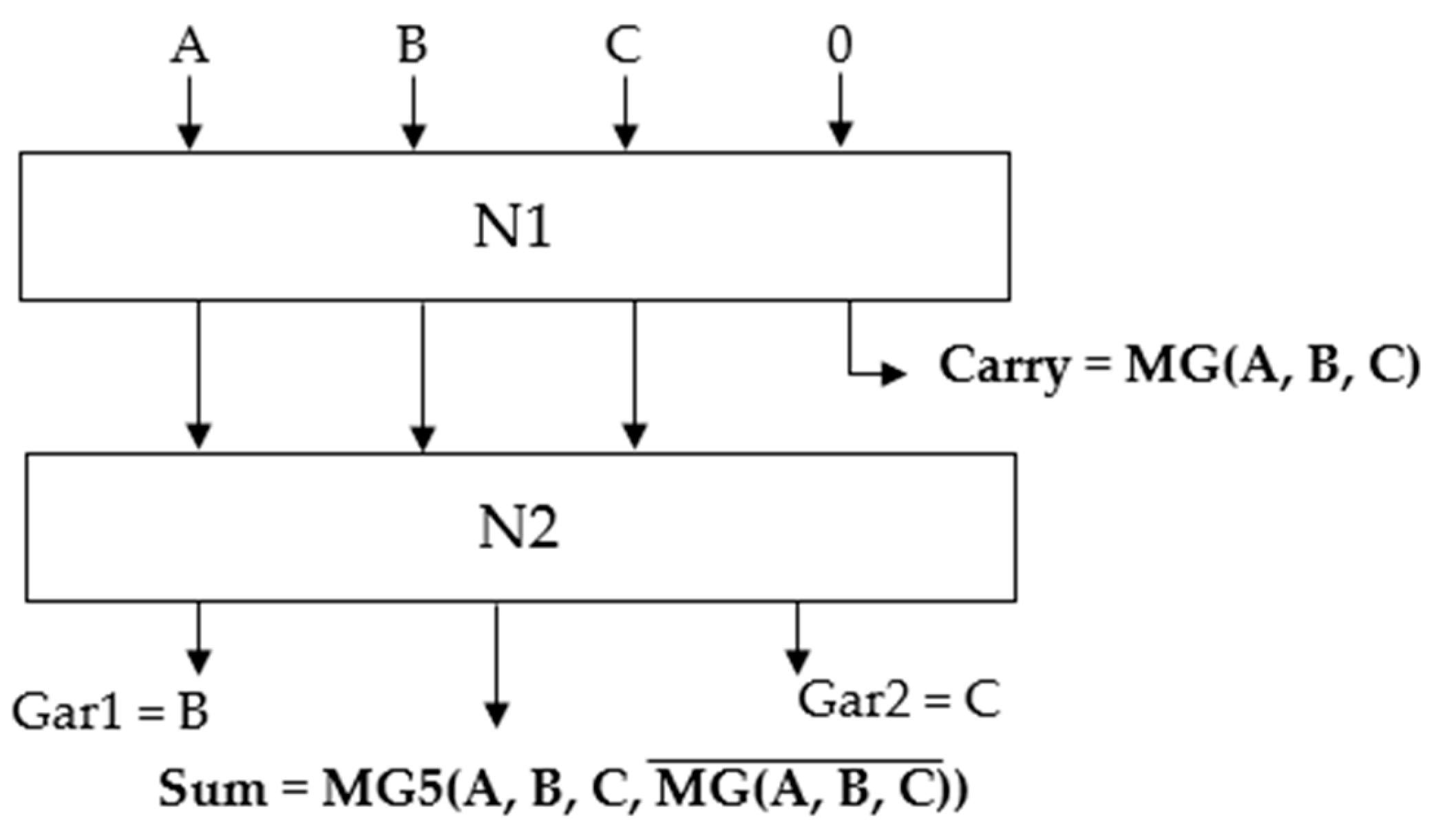
Figure 3 shows the logic diagram of the reversible full adder circuit proposed by Hashemi et al. [33]. They newly proposed two reversible gates, 4 × 4 N1 and 3 × 3 N2. The N1 gate uses a 3-input majority gate to output Carry, and the N2 gate uses a 5-input majority gate to output two garbage values and Sum.
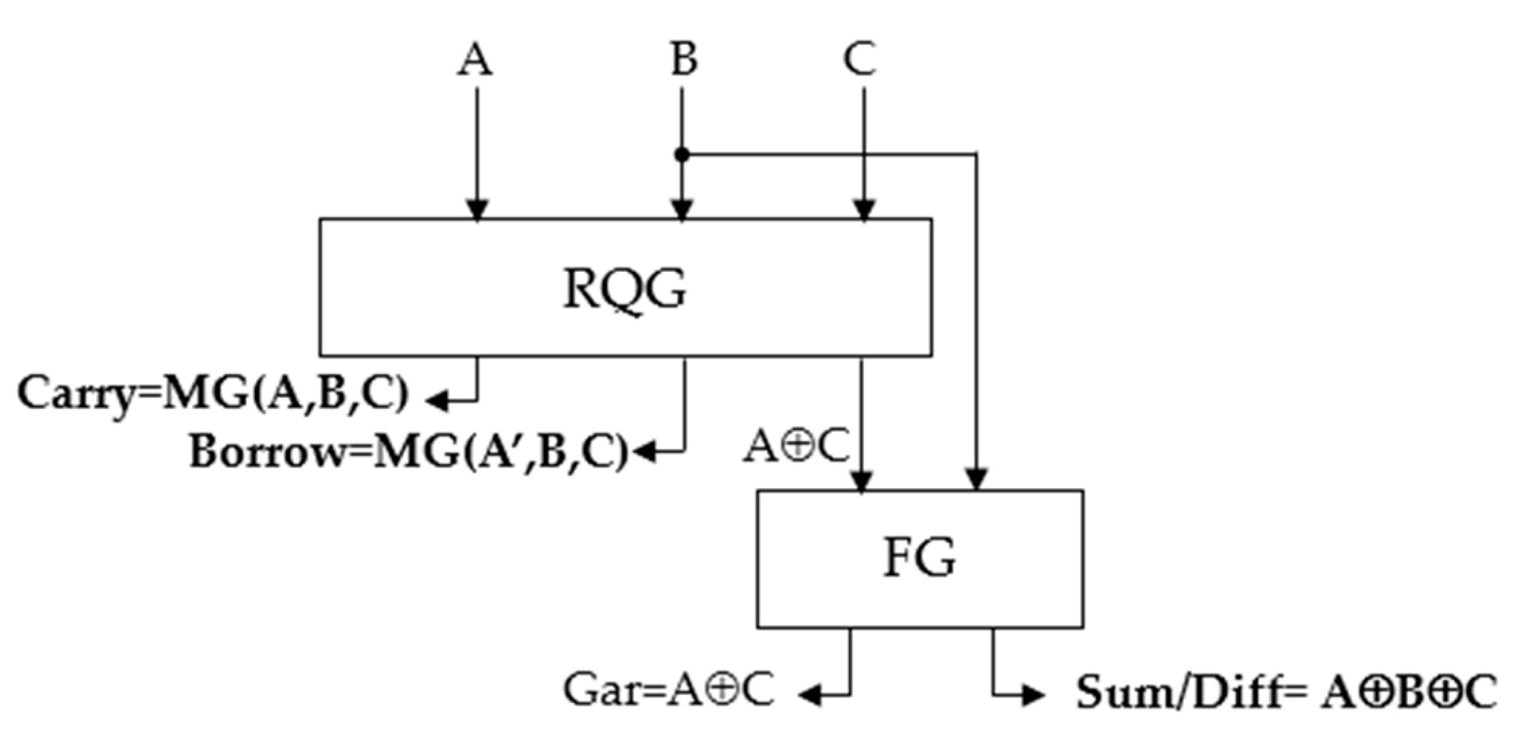
Taherkhani et al. developed a 3 × 3 RQG producing three outputs, M G ( A , B , C ) , M G ( A , B , C ) , and A B C , and proposed an RFAS circuit with two FGs [35]. The first FG was used to match the number of inputs and outputs for a reversible operation, and the second FG was used for an additional reversible XOR operation. Figure 4 shows the logic diagram of RFAS proposed by Taherkhani et al.
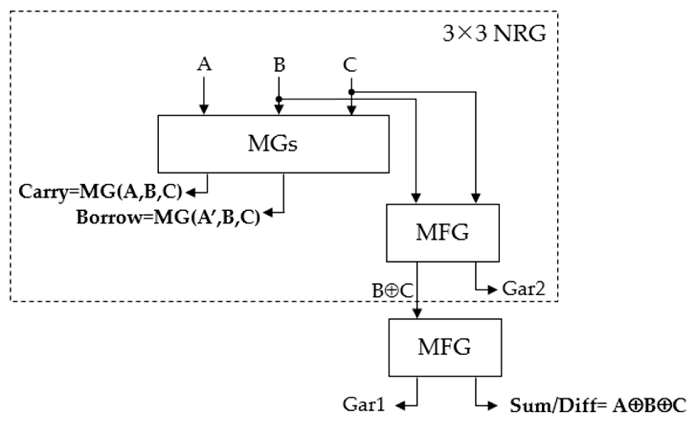
Ahmad et al. proposed a single-layer RFSA with 3 × 3 NRG and 2 × 2 MFG [36], as shown in Figure 5. The three inputs, A, B, and C, each pass through two MGs to produce output values Carry and Borrow. The MFG plays the same role as the FG and passes through two MFGs to output Sum/Diff, which is the output value of the full adder-subtractor.
Vahabi et al. recently proposed a circuit that improved the performance of RFAS using existing RQG. In the existing circuit, an attempt was made to minimize the overall area and delay by excluding the first FG and using a new XOR gate [37], as shown in Figure 6. However, because the number of inputs and outputs is different, it cannot function as a logical or physical reversible circuit.

3. Proposed Reversible Full Adder-Subtractor

This section shows the RFAS circuit proposed in this study. To effectively implement the proposed circuit, the 3-input XOR gate proposed in paper [42] is modified to a 2-input XOR gate. In addition, we implement the logic diagram of reversible RFAS based on RQG introduced in Figure 4. For this purpose, the QCA implementation of effective FG and RQG circuits is necessary.
Figure 7a implements the 2 × 2 FG using the proposed 2-input XOR gate using QCA. It has two inputs, A and B, and two outputs, P and Q. The value input to A can be directly output as the value of P, and the value of Q is output by the XOR operation of A and B. Figure 7b shows the QCA layout of RQG using one majority gate, one rotated majority gate, and the proposed 2-input XOR gate. At the center of the circuit is a rotated majority gate consisting of three inputs, A, B, and C, which produces the first result, P. A has the value A’ by the simple inverter located at the bottom, and the remaining inputs, B and C, meet at the majority gate located on the left side of the circuit to produce Q. At the same time, A and C produce the value of R by operating with the 2-input XOR gate located on the right side of the circuit.
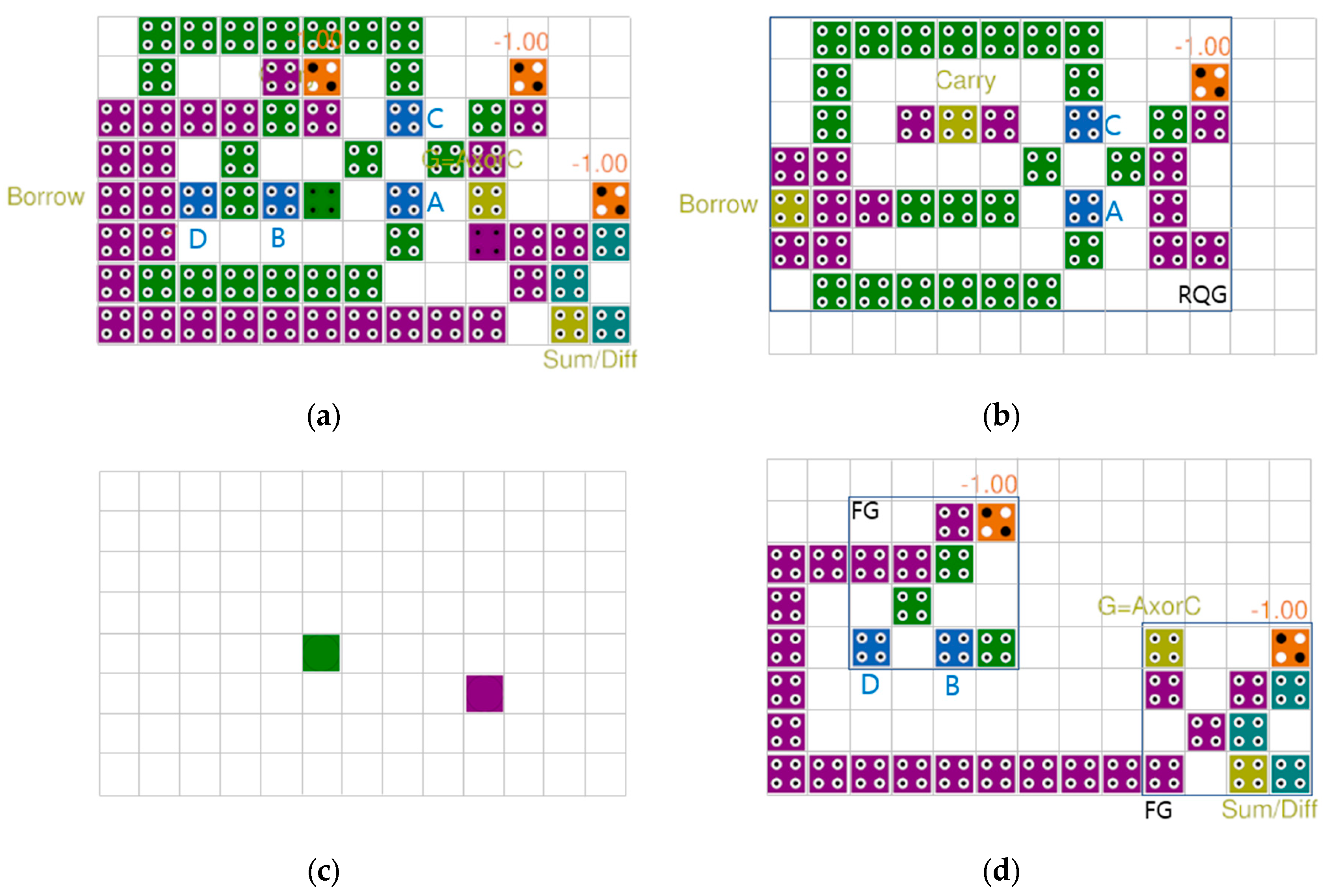
Figure 8 shows the QCA layout of the proposed multi-layered 4 × 4 RFAS circuit consisting of three layers. The first layer, as shown in Figure 8b, faithfully implements the RQG circuit shown in Figure 7b. Two FGs are implemented in the third layer of Figure 8d. Figure 8c serves as a bridge connecting the first and third layers. In the first clock phase, the input value B of the third layer crosses the bridge of the second layer and comes down to the first layer. In the second phase, the FG located on the left side of the circuit of the third layer outputs B as inputs of B and D, and transmits it to the input value of the FG on the right side of the circuit. At this time, the value of the A⊕C output from the first layer is transmitted to the input of the FG of the third layer through the bridge of the second layer, and Carry and Borrow are also output. Finally, in the third phase, Sum/Diff is output through the XOR operation on the two values input to FG.
Figure 9 shows the simulation results of the proposed RFAS. In Figure 9, it is confirmed that Carry and Borrow are output on CLOCK1, the second clock phase, and Sum/Diff are output on CLOCK2, the third clock phase. In addition, the RFAS circuit outputs normally, as shown in Table 2, and the output polarization is very high, up to 0.992, and a stable output signal without noise is confirmed. The following metrics are defined for performance comparison. Cell count refers to the number of cells required for circuit design, area refers to the rectangular area required for circuit design, and delay refers to the clock cycle (1 clock cycle = 4 clock phases) until the first output of the circuit is produced.

4. Simulation and Performance Analysis

In this section, QCADesigner 2.0.3 and its extended version, QCADesigner-E 2.2, are used to measure QCA performance and energy dissipation [43,44]. They each use “Bistable Approximation” and “Coherence Vector with Energy” as simulation engines, and the related parameters are summarized in Table 3.
Recently, with the rapid development of hardware, the importance of delay is evaluated more highly than area. Therefore, Equation (7) is the most commonly used cost calculation formula including area and delay [45,46]. Here, area and delay refer to the rectangular area and clock phase required for circuit design, respectively. In particular, the area of a multi-layer structure is the flat area multiplied by the number of layers. Equation (6) is applied to the area of a multilayer structure.
A r e a m u l t i l a y e r = A r e a s i n g l e l a y e r × m
where m is the number of layers on a multi-layer structure to reflect the higher area cost of a multi-layer design over a coplanar structure [24,45].
As shown in Table 4, the proposed circuit performs both reversible full adder and full subtractor, and has the best performance and cost in terms of number of cells, area, delay, and CostAD. Compared to the best existing structure in [37], it showed significant improvements of 67% and 180% in delay and CostAD. Due to the rapid development of hardware, delay is becoming more important than area, so CostAD is proportional to the square of delay.
C o s t A D = A × D 2
where A and D refers to the area and the delay of a circuit, respectively. Equation (8) is a standard design cost measurement method including energy dissipation and delay [44,45]. The importance of energy dissipation is viewed as being equal to delay, and CostED is proportional to the square of energy dissipation and the square of delay.
C o s t E D = E 2 × D 2
where E and D refers to the energy dissipation and the delay of a circuit, respectively [47]. Avg_Ebath and Sum_Ebath in Table 5 indicate the average energy dissipation per cycle and the total energy dissipation for all coordinates, respectively [48,49,50,51]. Both Avg_Ebath and Sum_Ebath showed an improvement of 54% compared to the existing circuit in [37], which had the lowest energy dissipation, and CostED achieved a remarkable reduction of 562%.
A O P = 1 n M a x   P o l a r i z a t i o n M i n   P o l a r i z a t i o n 2 n
The average output polarization (AOP) is an important indicator of the output strength of a circuit [48]. The output of a circuit with high AOP can stably transmit values to subsequent circuits, so it is one of the important performance indicators that is directly related to the scalability and connectivity of the circuit. AOP calculates the average of the highest and lowest values of output polarization, as shown in Equation (9) [52]. As shown in Table 6, the highest meaningful AOP of the proposed circuit was measured at all outputs. The total AOP, calculated as the average value of AOP of all outputs, improved by more than 3.8% compared to the best existing circuit in [37].

5. Conclusions

Recently, due to the development of quantum computers, much attention has been paid to the development and implementation of reversible gates. This is because effective implementation of reversible gates can accelerate the development of universal quantum computers and dramatically improve the performance of computing systems by minimizing energy and information loss. The proposed study constructed a FAS, one of the operation circuits that has the greatest impact on the performance of computing systems, as a circuit capable of reversible operation using QCA-based reversible gates. Although there have been QCA implementations for circuit design using various existing reversible gates, the RFAS using multilayer RQG proposed in this study was verified to be the best in all performance aspects such as area, delay, energy dissipation, and AOP required for circuit design. In addition, it demonstrated outstanding excellence in two standard design cost indicators compared to existing excellent circuits. The implementation of RFAS and reversible gates using multi-layer QCA can lead to many creative ideas and development of various circuits. However, it always has a weakness in the difficulty of actual implementation. With the rapid development of 3D stacked memories such as HBM in semiconductors, the feasibility of multilayer structures in QCA is increasing, and QCA technology will further develop through challenging research.

Funding

This research received no external funding.

Institutional Review Board Statement

Not applicable.

Informed Consent Statement

Not applicable.

Data Availability Statement

The original contributions presented in the study are included in the article, further inquiries can be directed to the corresponding author/s.

Conflicts of Interest

The author declares no conflicts of interest.

References

  1. Bilal, B.; Ahmed, S.; Kakkar, V. An insight into beyond CMOS Next generation computing using quantum-dot cellular automata nanotechnology. Int. J. Eng. Manuf. 2018, 8, 25–37. [Google Scholar] [CrossRef]
  2. Moore, G.E. No exponential is forever: But “Forever” can be delayed! [semiconductor industry]. In Proceedings of the 2003 IEEE International Solid-State Circuits Conference, 2003. Digest of Technical Papers, ISSCC, San Francisco, CA, USA, 13–13 February 2003; pp. 20–23. [Google Scholar]
  3. Dennard, R.H.; Gaensslen, F.H.; Kuhn, L.; Yu, H.N. Design of micron MOS switching devices. In Proceedings of the International Electron Devices Meeting, Washington, DC, USA, 4–6 January 1972; pp. 168–170. [Google Scholar]
  4. Iwai, H. Roadmap for 22 nm and beyond. Microelectron. Eng. 2009, 86, 1520–1528. [Google Scholar] [CrossRef]
  5. Landauer, R. Irreversibility and heat generation in the computing process. IBM J. Res. Dev. 1961, 5, 183–191. [Google Scholar] [CrossRef]
  6. Bennett, C.H. Logical reversibility of computation. IBM J. Res. Dev. 1973, 17, 525–532. [Google Scholar] [CrossRef]
  7. Song, Y.; Wu, Y.; Wu, S.; Li, D.; Wen, Q.; Qin, S.; Gao, F. A quantum federated learning framework for classical clients. Sci. China Phys. Mech. Astron. 2024, 67, 250311. [Google Scholar] [CrossRef]
  8. Toffoli, T. Reversible computing. In International Colloquium on Automata, Languages, and Programming; Springer: Berlin/Heidelberg, Germany, 1980; pp. 632–644. [Google Scholar]
  9. Barenco, A.; Bennett, C.H.; Cleve, R.; DiVincenzo, D.P.; Margolus, N.; Shor, P.; Sleator, T.; Smolin, J.A.; Weinfurter, H. Elementary gates for quantum computation. Phys. Rev. A 1995, 52, 3457–3467. [Google Scholar] [CrossRef] [PubMed]
  10. Fredkin, E.; Toffoli, T. Conservative Logic. Int. J. Theor. Phys. 1982, 21, 219–253. [Google Scholar] [CrossRef]
  11. Feynman, R. Quantum Mechanical Computers. Opt. News 1985, 11, 11–20. [Google Scholar] [CrossRef]
  12. Peres, A. Reversible logic and quantum computers. Phys. Rev. A 1985, 32, 3266–3276. [Google Scholar] [CrossRef]
  13. Sen, B.; Adak, T.; Anand, A.S.; Sikdar, B.K. Synthesis of reversible universal QCA gate structure for energy efficient digital design. In Proceedings of the IEEE Region 10 Conference TENCON, Bali, Indonesia, 21–24 November 2011; pp. 806–810. [Google Scholar]
  14. Sen, B.; Dutta, M.; Some, S.; Sikdar, B.K. Realizing Reversible Computing in QCA Framework Resulting in Efficient Design of Testable ALU. ACM J. Emerg. Technol. Comput. Syst. 2014, 11, 1–22. [Google Scholar] [CrossRef]
  15. Islam, M.S.; Abdullah-Al-Shafi, M.; Bahar, A.N. A new approach of presenting universal reversible gate in nanoscale. Int. J. Comput. Appl. 2016, 134, 1–4. [Google Scholar]
  16. Saravanan, S.; Vennila, I.; Mohanram, S. Design and Implementation of an Efficient Reversible Comparator Using TR Gate. Circuits Syst. 2016, 7, 2578–2592. [Google Scholar] [CrossRef]
  17. Chabi, A.M.; Roohi, A.; Khademolhosseini, H.; Sheikhfaal, S.; Angizi, S.; Navi, K.; De-Mara, R.F. Towards ultra-efficient QCA reversible circuits. Microprocess. Microsyst. 2017, 49, 127–138. [Google Scholar] [CrossRef]
  18. Moustafa, A.; Younes, A. Efficient Synthesis of Reversible Circuits Using Quantum Dot Cellular Automata. IEEE Access 2021, 9, 76662–76673. [Google Scholar] [CrossRef]
  19. Lent, C.; Tougaw, P. A device architecture for computing with quantum dots. Proc. IEEE 1997, 85, 541–557. [Google Scholar] [CrossRef]
  20. Srivastava, S.; Sarkar, S.; Bhanja, S. Power dissipation bounds and models for quantum-dot cellular automata circuits. In Proceedings of the 2006 Sixth IEEE Conference on Nanotechnology, Cincinnati, OH, US, 17–20 July 2006; Volume 1, pp. 375–378. [Google Scholar]
  21. Srivastava, S.; Sarkar, S.; Bhanja, S. Estimation of upper bound of power dissipation in QCA circuits. IEEE Trans. Nanotechnol. 2009, 8, 116–127. [Google Scholar] [CrossRef]
  22. Song, Z.; Xie, G.; Cheng, X.; Wang, L.; Zhang, Y. An Ultra-Low Cost Multilayer RAM in Quantum-Dot Cellular Automata. IEEE Trans. Circuits Syst. II Express Briefs 2020, 67, 3397–3401. [Google Scholar] [CrossRef]
  23. Heikalabad, S.R.; Salimzadeh, F.; Barughi, Y.Z. A unique three-layer full adder in quantum-dot cellular automata. Comput. Electr. Eng. 2020, 86, 106735. [Google Scholar] [CrossRef]
  24. Chu, Z.; Li, Z.; Xia, Y.; Wang, L.; Liu, W. BCD Adder Designs Based on Three-Input XOR and Majority Gates. IEEE Trans. Circuits Syst. II Express Briefs 2021, 68, 1942–1946. [Google Scholar] [CrossRef]
  25. Perri, S.; Spagnolo, F.; Frustaci, F.; Corsonello, P. Multibit Full Comparator Logic in Quantum-Dot Cellular Automata. IEEE Trans. Circuits Syst. II Express Briefs 2022, 69, 4508–4512. [Google Scholar] [CrossRef]
  26. Das, R.; Alam, M.S.; Ahmmed, K.T. An energy efficient design of a multi-layered crossover based 3:8 decoder using quantum-dot cellular automata. Heliyon 2022, 8, e11643. [Google Scholar] [CrossRef] [PubMed]
  27. Khan, A.; Parameshwara, M.C.; Arya, R. Defects of quantum dot cellular automata computing devices: An extensive review, evaluation, and future directions. Microprocess. Microsyst. 2023, 101, 104912. [Google Scholar] [CrossRef]
  28. Khan, A.; Bahar, A.N.; Arya, R. Quad-functioning Parity Layout for Nanocomputing: A QCA Design. Nano Commun. Netw. 2024, 41, 100525. [Google Scholar] [CrossRef]
  29. Safoev, N.; Jeon, J.C. A novel controllable inverter and adder/subtractor in quantum-dot cellular automata using cell interaction based XOR gate. Microelectron. Eng. 2020, 222, 111197. [Google Scholar] [CrossRef]
  30. Safoev, N.; Jeon, J.C. Design of high-performance QCA incrementer/decrementer circuit based on adder/subtractor methodology. Microprocess. Microsyst. 2020, 72, 102927. [Google Scholar] [CrossRef]
  31. Erniyazov, S.; Jeon, J.C. Carry save adder and carry look ahead adder using inverter chain based coplanar QCA full adder for low energy dissipation. Microelectron. Eng. 2019, 211, 37–43. [Google Scholar] [CrossRef]
  32. Kianpour, M.; Sabbaghi-Nadooshan, R. Novel 8-bit reversible full adder/subtractor using a QCA reversible gate. J. Comput. Electron. 2017, 16, 459–472. [Google Scholar] [CrossRef]
  33. Hashemi, S.; Azghadi, M.R.; Navi, K. Design and analysis of efficient QCA reversible adders. J. Supercomput. 2018, 75, 2106–2125. [Google Scholar] [CrossRef]
  34. Kumar, P.; Singh, S. Optimization of the area efficiency and robustness of a QCA-based reversible full adder. J. Comput. Electron. 2019, 18, 1478–1489. [Google Scholar] [CrossRef]
  35. Taherkhani, E.; Moaiyeri, M.H.; Angizi, S. Design of an ultra-efficient reversible full adder-subtractor in quantum-dot cellular automata. Optik 2017, 142, 557–563. [Google Scholar] [CrossRef]
  36. Ahmad, F.; Ahmed, S.; Kakkar, V.; Bhat, G.M.; Bahar, A.N.; Wani, S. Modular Design of Ultra-Efficient Reversible Full Adder-Subtractor in QCA with Power Dissipation Analysis. Int. J. Theor. Phys. 2018, 57, 2863–2880. [Google Scholar] [CrossRef]
  37. Vahabi, M.; Rahimi, E.; Lyakhov, P.; Bahar, A.N.; Wahid, K.A.; Otsuki, A. Novel Quan-tum-Dot Cellular Automata-Based Gate Designs for Efficient Reversible Computing. Sustainability 2023, 15, 2265. [Google Scholar] [CrossRef]
  38. Lent, C.S.; Tougaw, P.D.; Porod, W. Quantum cellular automata: The physics of computing with arrays of quantum dot molecules. In Proceedings of the Workshop on Physics and Computation, PhysComp ‘94, Dallas, TX, USA, 17–20 November 1994; pp. 5–13. [Google Scholar]
  39. Lent, C.S.; Tougaw, P.D. Logical devices implemented using quantum cellular automata. J. Appl. Phys. 1993, 75, 1818–1825. [Google Scholar]
  40. Jeon, J.C. “Multi-Layer QCA Shift Registers and Wiring Structure for LFSR in Stream Cipher with Low Energy Dissipation in Quantum Nanotechnology. Electronics 2023, 12, 4093. [Google Scholar] [CrossRef]
  41. Hosseinzadeh, M.; Hussain, D.; Azimi, N.; Alenizi, F.A.; Safaiezadeh, B.; Ahmed, O.H.; Lee, S.-W.; Rahmani, A.M. Design and simulation of Full-Subtractor based on Quantum-Dot cellular automata technology. AEU—Int. J. Electron. Commun. 2023, 171, 154927. [Google Scholar] [CrossRef]
  42. Abutaleb, M.M. Utilizing charge reconfigurations of quantum-dot cells in building blocks to design nanoelectronic adder circuits. Comput. Electr. Eng. 2020, 86, 106712. [Google Scholar] [CrossRef]
  43. Walus, K.; Dysart, T.J.; Jullien, G.A.; Budiman, R.A. QCADesigner: A rapid design and simulation tool for quantum-dot cellular automata. IEEE Trans. Nanotechnol. 2004, 3, 26–31. [Google Scholar] [CrossRef]
  44. QCADesigner-E. Available online: https://github.com/FSillT/QCADesigner-E (accessed on 18 August 2024).
  45. Liu, W.; Lu, L.; O’Neill, M.; Swartzlander, E.E. A First Step toward Cost Functions for Quantum-Dot Cellular Automata Designs. IEEE Trans. Nanotechnol. 2014, 12, 476–487. [Google Scholar]
  46. Seo, D.K.; Jeon, J.C. QCA-Based Secure RAM Cell Structure Using Logic Transformation and Cell Interaction with Signal Reliability and Energy Dissipation in Quantum Computing. Appl. Sci. 2023, 13, 9998. [Google Scholar] [CrossRef]
  47. Jeon, J.C. Quantum-Dot CA-Based Fredkin Gate and Conservative D-latch for Reliability-Based Information Transmission on Reversible Computing. Electronics 2024, 13, 2872. [Google Scholar] [CrossRef]
  48. Timler, J.; Lent, C.S. Power gain and dissipation in quantum-dot cellular automata. J. Appl. Phys. 2002, 91, 823–831. [Google Scholar] [CrossRef]
  49. Torres, F.S.; Wille, R.; Niemann, P.; Drechsler, R. An Energy-Aware Model for the Logic Synthesis of Quantum-Dot Cellular Automata. IEEE Trans. Comput.-Aided Des. Integr. Circuits Syst. 2018, 37, 3031–3041. [Google Scholar] [CrossRef]
  50. Jeon, J.C. Low-complexity QCA universal shift register design using multiplexer and D flip-flop based on electronic correlations. J. Supercomput. 2020, 76, 6438–6452. [Google Scholar] [CrossRef]
  51. Jeon, J.C. Designing nanotechnology QCA–multiplexer using majority function-based NAND for quantum computing. J. Supercomput. 2021, 77, 1562–1578. [Google Scholar] [CrossRef]
  52. Abdullah-Al-Shafi, M.; Bahar, A.N.; Bhuiyan, M.M.R.; Shamim, S.M.; Ahmed, K. Average out-put polarization dataset for signifying the temperature influence for QCA designed reversible logic circuits. Data Brief 2018, 19, 42–48. [Google Scholar] [CrossRef]
Figure 1. QCA logic gates: (a) 3-input majority gate; (b) AND gate; (c) OR gate; (d) rotated 3-input majority gate; (e) robust NOT gate; (f) simple NOT gate.
Applsci 14 08886 g001
Figure 2. Four states of the QCA clock.
Applsci 14 08886 g002
Figure 3. Logic diagram of RFA proposed by Hashemi et al. [33].
Applsci 14 08886 g003
Figure 4. Logic diagram of RFAS proposed by Taherkhani et al. [35].
Applsci 14 08886 g004
Figure 5. Logic diagram of RFAS proposed by Ahmad et al. [36].
Applsci 14 08886 g005
Figure 6. Logic diagram of RFAS proposed by Ahmad et al. [37].
Applsci 14 08886 g006
Figure 7. Proposed QCA implementation of reversible gates: (a) FG; (b) RQG.
Applsci 14 08886 g007
Figure 8. QCA implementation of the proposed RFAS: (a) top view; (b) first layer; (c) second layer; (d) third layer.
Applsci 14 08886 g008
Figure 9. Simulation results of the proposed RFAS circuit.
Applsci 14 08886 g009
Table 1. Major contributions to the development of RFA(S).
ReferenceYearStructureMajor Contributions
[32]2017RFAS3 × 3 QCA Reversible (QR) gate using Toffoli and Fredkin gates
[33]2018RFA4 × 4 N1 and 3 × 3 N2 gates based on a 5-input majority gate
[34]2019RFAArea optimization using a 5-input majority gate
[35]2017RFAS3 × 3 Reversible Quantum Gate (RQG)
[36]2018RFAS3 × 3-New Reversible Gate (NRG) and Modified Feynman Gate (MFG)
[37]2023RFASOptimization of RQG
Table 2. Truth table of RFAS.
InputsOutputs
ABCCarryBorrowSum/Diff
000000
001011
010011
011110
100001
101100
110100
111111
Table 3. Simulation engines and parameters.
QCADesigner 2.0.3QCADesigner-E 2.2
ParametersBistable ApproximationCoherence Vector with Energy
Cell size (nm)1818
Dot diameter (nm)55
Cell separation (nm)22
Layer separation (nm)11.511.5
Clock high (J)9.8 × 10−229.8 × 10⁻²²
Clock low (J)3.8 × 10−233.8 × 10⁻²³
Clock shift00
Clock amplitude factor2.02.0
Relative permittivity12.912.9
Radius of effect (nm)6580
Number of samples12,800-
Convergence tolerance1.0 × 10−3-
Maximum iterations per sample100-
Temperature (K)-1
Relaxation time (s)-1.0 × 10⁻¹⁵
Clock slope (s)-1.0 × 10⁻¹²
Time step (s)-1.0 × 10⁻¹⁶
Clock/input period (s)-4.0 × 10⁻¹²
Table 4. Performance comparison of RFA(S) circuits.
CircuitCell CountAreaDelayCostADOperation
no.Ratioµm2RatioClockRatioAD2Ratio
[32]3995.180.504.222.672.0029.6RFAS
[33]2363.060.322.73.254.333.3850.1RFA
[34]1782.310.231.93.254.332.4336.0RFA
[35]2282.960.282.31.752.330.8612.7RFAS
[36]1211.570.141.21.251.670.223.2RFAS
[37]1231.600.121.01.251.670.192.8RFAS
Ours771.000.121.00.751.000.071.0RFAS
Table 5. Energy dissipations and CostED comparison of RFA(S) circuits.
CircuitAvg_EbathError_AvgSum_EbathError_SumCostED
10−3 eVRatio−10−4 eVRatio10−2 eVRatio−10−3 eVRatioE2D2Ratio
[33]5.392.744.212.525.932.734.632.52371.43140.23
[34]4.902.493.952.375.382.484.352.36305.73115.42
[35]4.662.373.452.075.132.363.792.0680.6030.43
[36]3.521.793.011.803.871.783.311.8023.408.83
[37]3.041.542.491.493.351.542.741.4917.546.62
Ours1.971.001.671.002.171.001.841.002.651.00
Table 6. Average output polarization of RFA(S) circuits.
CircuitCarryBorrowSum/DiffTotal
AOPRatioAOPRatioAOPRatioAOPRatio
[33]9.5400.967--9.5500.9699.5450.966
[34]9.5400.967--9.5500.9699.5450.966
[35]9.5400.9679.5500.9639.5400.9689.5430.966
[36]9.5400.9679.5300.9619.5300.9679.5330.965
[37]9.5400.9679.5300.9619.4750.9619.5150.963
Ours9.8701.0009.9201.0009.8601.0009.8831.000
Disclaimer/Publisher’s Note: The statements, opinions and data contained in all publications are solely those of the individual author(s) and contributor(s) and not of MDPI and/or the editor(s). MDPI and/or the editor(s) disclaim responsibility for any injury to people or property resulting from any ideas, methods, instructions or products referred to in the content.