1. Introduction
The International Technology and Roadmap for Semiconductors (ITRS) points out major problems with existing CMOS technology, such as high-power loss, threshold voltages, thermal runaway, and high leakage current, and states that it is approaching the end of its semiconductor nano-system roadmap [
1]. Moore’s law, which states that the number of components on a single chip doubles approximately every two years [
2], no longer applies in nanoscale devices, and various quantum mechanical effects dominate device physics [
3]. In addition, as CMOS-VLSI micro technology reduces the size of transistors disproportionately, large energy and information losses are emerging as major problems. Information loss is a major problem in irreversible digital computation systems, and there is a large and growing demand for nanoscale computation systems that can minimize heat dissipation [
4].
Therefore, the design of reversible circuits is a key structural engineering challenge for solving the problem of information loss while minimizing energy dissipation. Landauer demonstrated that 1-bit information loss results in energy dissipation of
kBTln2 joules, where
kB = 1.38 × 10
−23 JK
−1 is the Boltzmann constant and
T is the temperature in Kelvin [
5]. At room temperature (
T = 300 K), the heat release occurring during a binary transaction is 0.017 eV and is considered physically irreversible, and this microscopic physical state can be restored to what it was before the process occurred. Bennett demonstrated the validity that energy loss of
kBTln2 joules in an irreversible circuit can be recovered in a reversible circuit [
6].
Recently, with the rapid rise of quantum computing [
7], quantum logic gates are attracting attention as logic gates that can replace existing digital circuits in quantum circuit calculation models. The Toffoli gate, developed in 1980, is a universal gate that can implement any desired Boolean function as a reversible circuit [
8], and it can be realized by five two-qubit quantum gates [
9]. Along with this, various universal reversible gates, such as the Fredkin gate, Feynman gate, and Peres, were developed [
10,
11,
12]. Since then, various reversible gates, such as RUG [
13], RQCA [
14], URG [
15], TR [
16], and PQR [
17], have been continuously developed and implemented using QCA [
18].
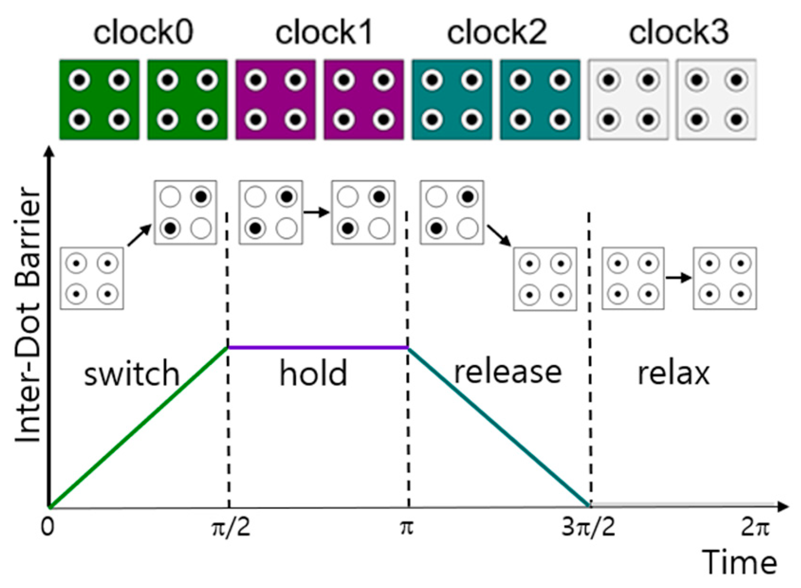
Quantum-dot cellular automata (QCA), proposed by Lent and Tougaw, has emerged as an alternative to overcome the problems of existing CMOS and implements existing reversible circuits with ultra-low power consumption. The dissipated energy is measured based on the Hamiltonian matrix, using the HartreeFock approximation in relation to the Coulomb repulsion between QCA cells, as shown in (1) [
19].
where
is the energy cost of two neighboring cells with opposite polarization, called kink energy,
denotes the polarization of the
i-th neighboring cell, and
denotes the geometrical factor identifying the electrostatic interaction between cells
i and
j due to the geometrical distance. This kink energy is related to the energy cost of two cells with the opposite polarization. γ denotes the electron tunneling energy inside the cell, which is controlled by the clock. The nonadiabatic power estimation model was used to estimate the power loss or energy dissipation of the cell [
20,
21]. The expected value of the Hamiltonian at each time instant is given by
where
is the 3-D energy vector, and
is the coherence vector. Based on (2), the equation for instantaneous power is given as (3).
The first term in (4) represents the power going in and out of the clock and inter-cell power flow, and the second term represents the power dissipated. By multiplying these two terms, the power dissipation at a specific time can be obtained.
Therefore, power dissipation can be summarized in terms of energy per clock cycle, as shown in (5).
where
is the clock period and
and
are the Hamiltonian values before and after the transaction processing.
Multilayer structures are a design method that minimizes energy dissipation and are a field of QCA design that is being studied extensively. Although feasibility is lower and design cost is higher than that of a co-planar structure, a well-designed multi-layer structure plays a significant role in minimizing space, delay, and energy consumption, and is continuously being studied at various major universities and research institutes. In 2020, Song et al. [
22] and Heikalabad et al. [
23] proposed a QCA-based RAM and full adder using a multi-layer structure, respectively, and in 2021, Chu et al. proposed a 3-input XOR-based QCA BCD adder using a multi-layer structure [
24]. In 2022, Perri et al. [
25] and Das et al. [
26] proposed a QCA multi-bit comparator and a 3:8 decoder using a multi-layer crossover, respectively.
In 2023 and 2024, Khan et al. presented various analyses of the latest trends and problems related to QCA design [
27,
28]. In particular, much research has been conducted based on QCA on the full adder-subtractor (FAS), the core circuit of the ALU, which consumes the most power in computer processors [
29,
30,
31], and research on reversible FAS (RFAS) continues to minimize energy dissipation. Recently, various reversible gates have been implemented using QCA.
Kianpour et al. designed a Toffoli gate and a Fredkin gate using a rotated QCA cell and proposed RFAS based on a QR gate using these gates [
32]. Hashemi et al. and Kumar et al. proposed RFA without a subtractor along with a new reversible gate using a QCA-based 3-input majority gate and a 5-input majority gate, respectively [
33,
34]. Taherkhani et al. proposed a more efficient RFAS using the newly proposed reversible QCA gate (RQG) and two Feynman gates (FGs) [
35], and Ahmad et al. developed a new reversible gate (NRG) using QCA-based multiple gates and FG, and proposed NRG-based RFAS [
36]. Vahabi efficiently redesigned various reversible gates using QCA and proposed RFAS with excellent performance using the existing RQG [
37].
Table 1 summarizes the major contributions to the development of RFA(S).
In this study, we review previously proposed QCA-based RFAS circuits and propose the most efficient RFAS that improves the problems of the circuits using QCA. The contributions of this study are summarized as follows.
Review of the structure, operation, and characteristics of existing excellent QCA-based RFAS circuits
Design of a reversible quantum gate (RQG)-based RFAS after presenting the problems of implementing the existing QCA circuits
Best performance in all aspects compared with the existing circuits and significant improvements of at least 67% and 54% in delay and energy dissipation, respectively.
Remarkable improvements of 180% and 562% in two representative design costs, CostAD and CostED, respectively, compared to the best existing circuit
Noise-free and high and stable output polarization, especially a significant improvement of 3.8% in the average output polarization
Proposal of an efficient QCA-based RFAS that minimizes information loss and provides reliable information transmission through the best performance of the proposed reversible circuit
The structure of the paper is as follows.
Section 2 explains the basic operation principle of QCA and reviews existing QCA reversible full adder-subtractors.
Section 3 explains the operation and structure of the proposed reversible full adder-subtractor.
Section 4 analyzes and compares the results through simulations.
Section 5 concludes.
3. Proposed Reversible Full Adder-Subtractor
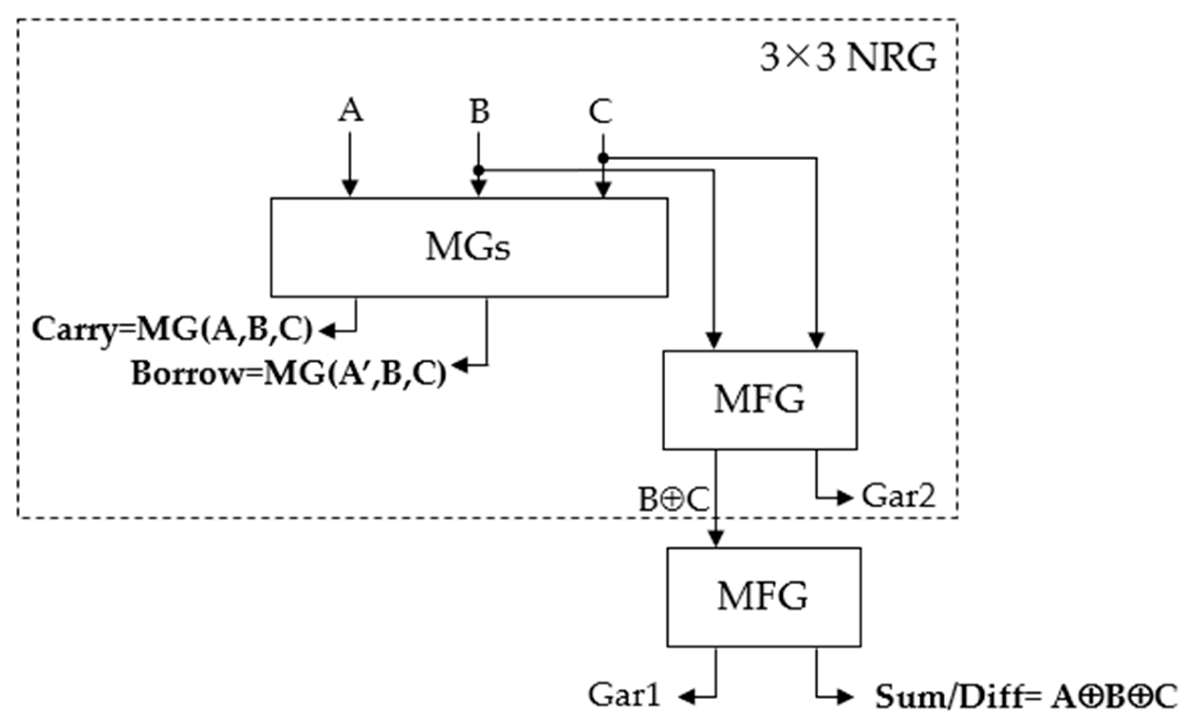
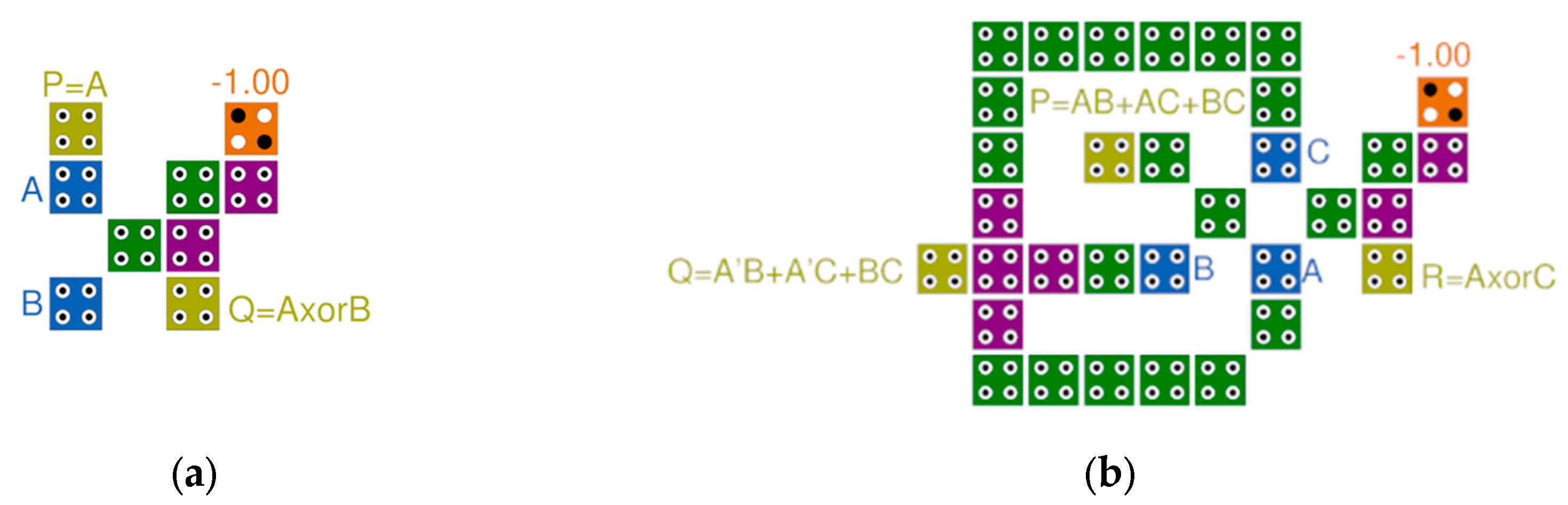
This section shows the RFAS circuit proposed in this study. To effectively implement the proposed circuit, the 3-input XOR gate proposed in paper [
42] is modified to a 2-input XOR gate. In addition, we implement the logic diagram of reversible RFAS based on RQG introduced in
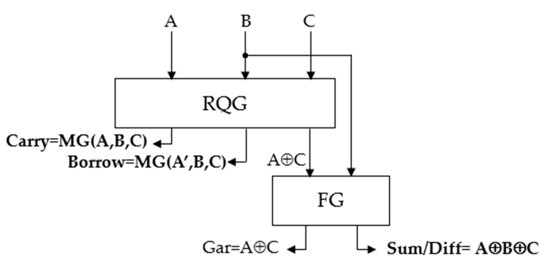
Figure 4. For this purpose, the QCA implementation of effective FG and RQG circuits is necessary.
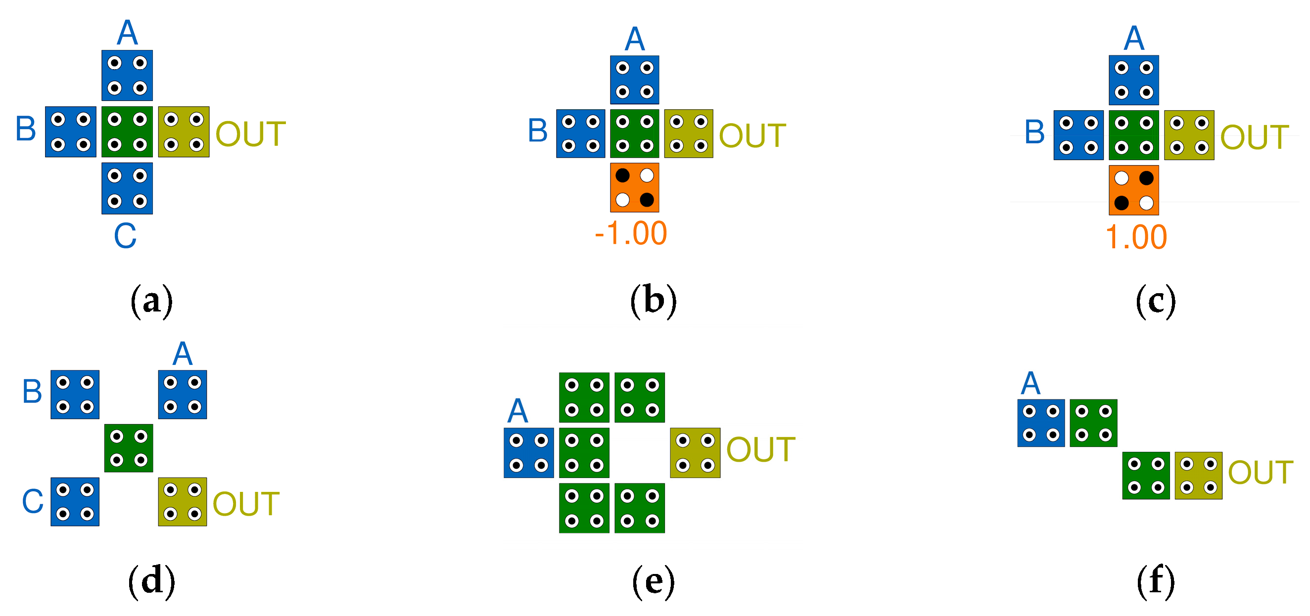
Figure 7a implements the 2 × 2 FG using the proposed 2-input XOR gate using QCA. It has two inputs, A and B, and two outputs, P and Q. The value input to A can be directly output as the value of P, and the value of Q is output by the XOR operation of A and B.
Figure 7b shows the QCA layout of RQG using one majority gate, one rotated majority gate, and the proposed 2-input XOR gate. At the center of the circuit is a rotated majority gate consisting of three inputs, A, B, and C, which produces the first result, P. A has the value A’ by the simple inverter located at the bottom, and the remaining inputs, B and C, meet at the majority gate located on the left side of the circuit to produce Q. At the same time, A and C produce the value of R by operating with the 2-input XOR gate located on the right side of the circuit.
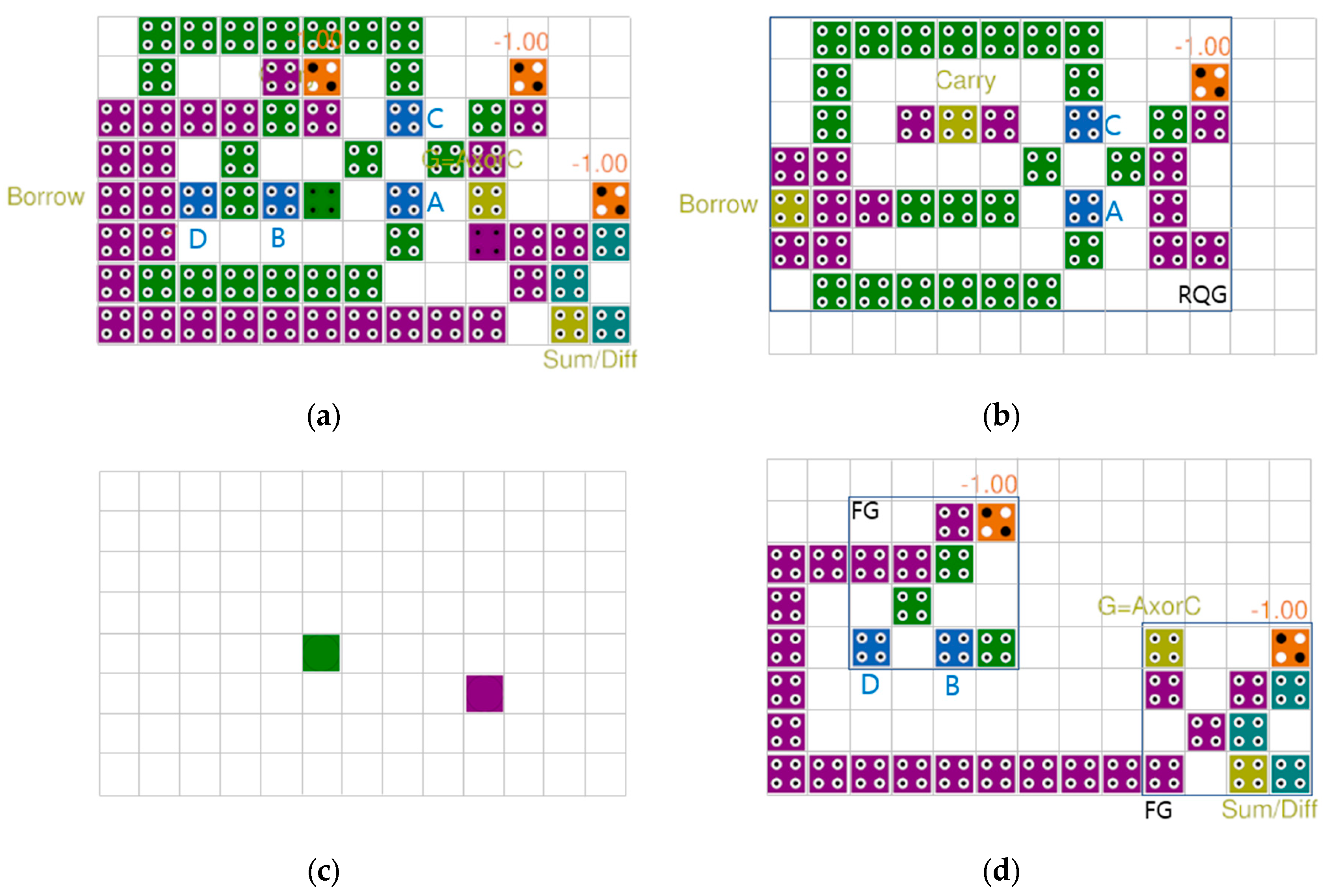
Figure 8 shows the QCA layout of the proposed multi-layered 4 × 4 RFAS circuit consisting of three layers. The first layer, as shown in
Figure 8b, faithfully implements the RQG circuit shown in
Figure 7b. Two FGs are implemented in the third layer of
Figure 8d.
Figure 8c serves as a bridge connecting the first and third layers. In the first clock phase, the input value B of the third layer crosses the bridge of the second layer and comes down to the first layer. In the second phase, the FG located on the left side of the circuit of the third layer outputs B as inputs of B and D, and transmits it to the input value of the FG on the right side of the circuit. At this time, the value of the A⊕C output from the first layer is transmitted to the input of the FG of the third layer through the bridge of the second layer, and Carry and Borrow are also output. Finally, in the third phase, Sum/Diff is output through the XOR operation on the two values input to FG.
Figure 9 shows the simulation results of the proposed RFAS. In
Figure 9, it is confirmed that Carry and Borrow are output on CLOCK1, the second clock phase, and Sum/Diff are output on CLOCK2, the third clock phase. In addition, the RFAS circuit outputs normally, as shown in
Table 2, and the output polarization is very high, up to 0.992, and a stable output signal without noise is confirmed. The following metrics are defined for performance comparison. Cell count refers to the number of cells required for circuit design, area refers to the rectangular area required for circuit design, and delay refers to the clock cycle (1 clock cycle = 4 clock phases) until the first output of the circuit is produced.
4. Simulation and Performance Analysis
In this section, QCADesigner 2.0.3 and its extended version, QCADesigner-E 2.2, are used to measure QCA performance and energy dissipation [
43,
44]. They each use “Bistable Approximation” and “Coherence Vector with Energy” as simulation engines, and the related parameters are summarized in
Table 3.
Recently, with the rapid development of hardware, the importance of delay is evaluated more highly than area. Therefore, Equation (7) is the most commonly used cost calculation formula including area and delay [
45,
46]. Here, area and delay refer to the rectangular area and clock phase required for circuit design, respectively. In particular, the area of a multi-layer structure is the flat area multiplied by the number of layers. Equation (6) is applied to the area of a multilayer structure.
where
m is the number of layers on a multi-layer structure to reflect the higher area cost of a multi-layer design over a coplanar structure [
24,
45].
As shown in
Table 4, the proposed circuit performs both reversible full adder and full subtractor, and has the best performance and cost in terms of number of cells, area, delay, and
CostAD. Compared to the best existing structure in [
37], it showed significant improvements of 67% and 180% in delay and
CostAD. Due to the rapid development of hardware, delay is becoming more important than area, so
CostAD is proportional to the square of delay.
where
and
refers to the area and the delay of a circuit, respectively. Equation (8) is a standard design cost measurement method including energy dissipation and delay [
44,
45]. The importance of energy dissipation is viewed as being equal to delay, and
CostED is proportional to the square of energy dissipation and the square of delay.
where
and
refers to the energy dissipation and the delay of a circuit, respectively [
47]. Avg_Ebath and Sum_Ebath in
Table 5 indicate the average energy dissipation per cycle and the total energy dissipation for all coordinates, respectively [
48,
49,
50,
51]. Both Avg_Ebath and Sum_Ebath showed an improvement of 54% compared to the existing circuit in [
37], which had the lowest energy dissipation, and
CostED achieved a remarkable reduction of 562%.
The average output polarization (AOP) is an important indicator of the output strength of a circuit [
48]. The output of a circuit with high AOP can stably transmit values to subsequent circuits, so it is one of the important performance indicators that is directly related to the scalability and connectivity of the circuit. AOP calculates the average of the highest and lowest values of output polarization, as shown in Equation (9) [
52]. As shown in
Table 6, the highest meaningful AOP of the proposed circuit was measured at all outputs. The total AOP, calculated as the average value of AOP of all outputs, improved by more than 3.8% compared to the best existing circuit in [
37].


