Abstract
With the advancement of CMOS technology, the susceptibility of SRAM to single node upset (SNU), double node upset (DNU), and multiple node upset (MNU) induced by radiation has increased. To address this issue, various cutting-edge solutions, such as radiation hardened sextuple cross coupled (RHSCC)-16T and DNU-completely-tolerant memory (DNUCTM) cells, have been proposed. While the RHSCC-16T cell is robust against SNU, it may be vulnerable to DNU. The DNUCTM cell is resistant to both SNU and DNU, but it remains susceptible to MNU. In this paper, we propose a radiation hardened read-stability and speed enhanced (RHRSE)-20T SRAM, which is immune to all potential cases of SNU, DNU, and MNU. Additionally, the proposed design demonstrates improvements in read and write delays compared to conventional SRAM designs. Experimental results confirm that the RHRSE-20T SRAM maintains stability under various charge levels for SEU, DNU, and MNU. The proposed integrated circuit is implemented in a 90-nm CMOS process and operates on a 1 V supply voltage, offering significant advantages for next-generation radiation-hardened memory applications.
1. Introduction
SRAM plays a crucial role in modern digital systems, ranging from embedded systems to high-performance computing applications. Due to its high speed, low latency, and ease of integration with logic circuits, SRAM is an essential component of contemporary semiconductor technology. According to the International Roadmap for Devices and Systems (IRDS) 2023, CMOS technology is expected to continue advancing, reaching approximately 2 nm by 2025, which is predicted to improve circuit performance [1].
With these advancements in CMOS technology, SRAM cells are shrinking in size each year, increasing the density of SRAM. As transistor sizes decrease, node capacitance naturally diminishes. Additionally, supply voltage is reduced to lower power consumption and mitigate thermal issues. Consequently, the amount of critical charge stored in circuit nodes decreases, making SRAM increasingly susceptible to soft errors caused by particle strikes such as protons, neutrons, electrons, muons, and alpha particles. These soft errors can destroy the information stored in memory elements, posing a significant threat to terrestrial electronic devices [2].
When a particle strikes a sensitive node in the circuit, the collected charge can generate a transient pulse known as a single event transient (SET). An SET can affect the charge state of the memory cell or the stored data bit, causing the node to retain an incorrect logic value, known as a single node upset (SNU). Moreover, with the increased integration density of circuits due to advances in CMOS manufacturing technology, a single radiation particle can simultaneously strike multiple memory cells. This can lead to a double node upset (DNU), where two nodes are simultaneously affected, or a multiple node upset (MNU), where three or more nodes are impacted [3,4,5].
Various radiation-hardened SRAM designs have been proposed to mitigate the soft error issues caused by radiation effects. For example, the We-Quatro SRAM employs additional negative feedback paths to improve the data stored in nodes affected by radiation [6]. However, this design is not fully immune to all cases of SNU and faces issues with write failures at low voltages. The radiation hardened sextuple cross coupled (RHSCC)-16T cell, which uses two storage nodes and four internal nodes, is fully immune to SNU but not entirely immune to DNU [7]. The QUCCE12T, composed of four cross-coupled input-split inverters, forms a large error-tolerant feedback loop to robustly maintain the stored value, but it also cannot withstand all cases of DNU [8]. The DNU-completely-tolerant memory (DNUCTM) design uses six access transistors, resulting in a relatively low read/write delay. Additionally, by spacing specific nodes apart in the layout, it is fully immune to DNU. However, because all nodes are sensitive, it does not fully recover from MNU despite the layout techniques [9]. The quadruple cross-coupled SRAM (QCCS) design demonstrates low read/write delays by using access transistors for both storage nodes and internal nodes, but it is not entirely immune to DNU. The sextuple cross-coupled SRAM(SCCS) can self-recover from all cases of DNU, but due to the use of many internal nodes, it is not fully immune to MNU [10]. The RSP14T improves SEU immunity and reduces leakage power but still struggles with high leakage [11]. To address SEMNU resistance, the RHD12T was proposed as a cell which can recover from SEMNU in specific internal node pairs [12]. However, it still cannot recover SEUs at nodes storing ‘0’ and has a higher leakage power compared to other designs. In an effort to minimize SEMNU, the RHPD14T was introduced, using a polar design to make certain nodes less vulnerable to SEU [13]. Despite its improved write performance, this design has the highest leakage power and the lowest read stability among the discussed cells.
In this paper, we propose the radiation hardened read-stability and speed enhanced (RHRSE)-20T design to address several challenges. The key contributions of this study are as follows. First, the proposed RHRSE-20T is resistant to various cases of single-node upsets (SNU) and, through advanced layout techniques, significantly enhances its immunity to dual-node and multi-node upsets (DNU and MNU), representing a major improvement over existing designs. Second, performance evaluations indicate that the read/write delay of the proposed design is not only shorter than that of various current designs but also maintains superior stability during both read and write operations, setting a new benchmark in radiation-hardened SRAM technology. These innovative features allow for efficient power consumption without compromising performance, thereby ensuring long-term reliability in high-radiation environments.
2. Proposed RHRSE-20T SRAM
2.1. Architecture
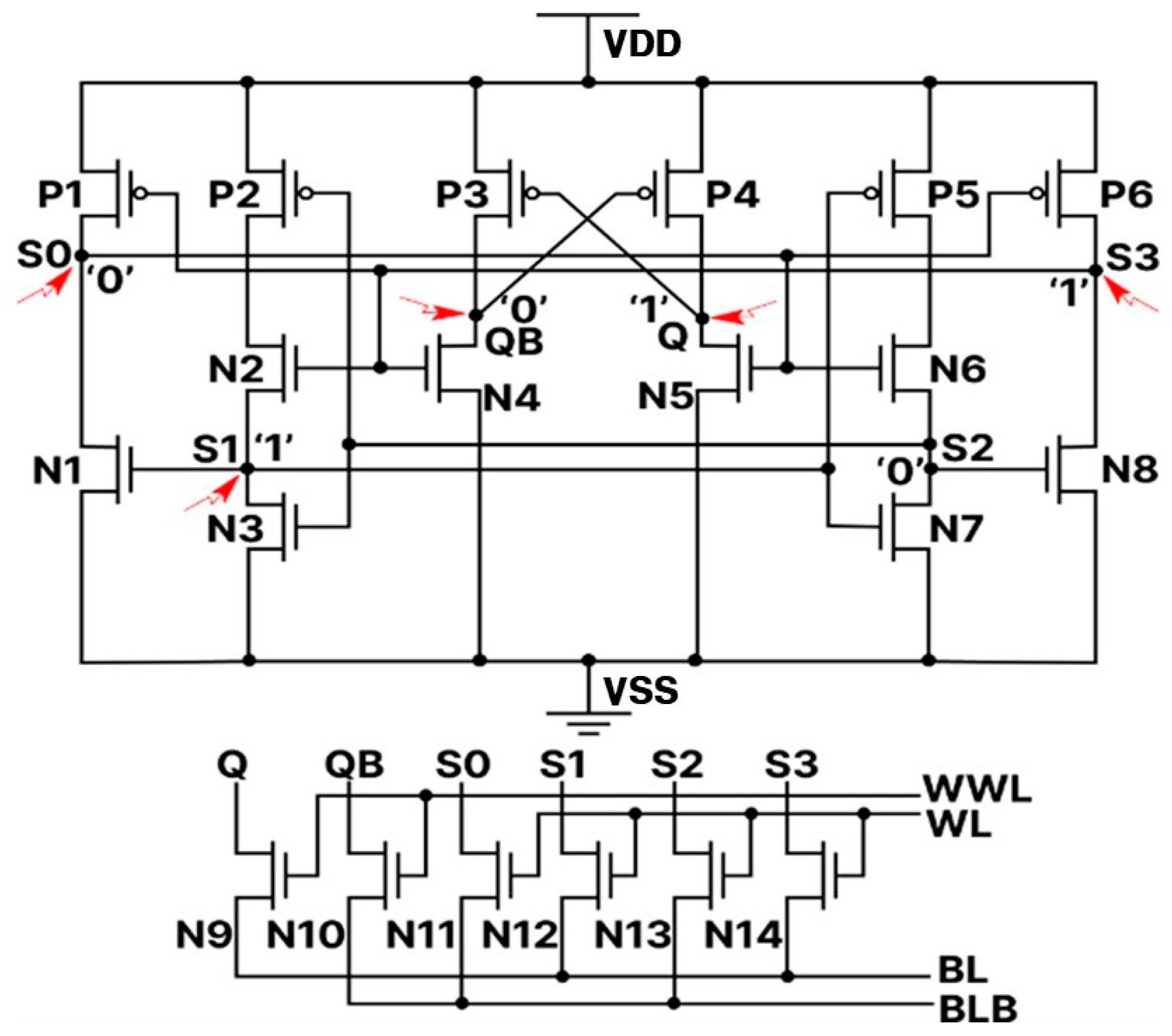
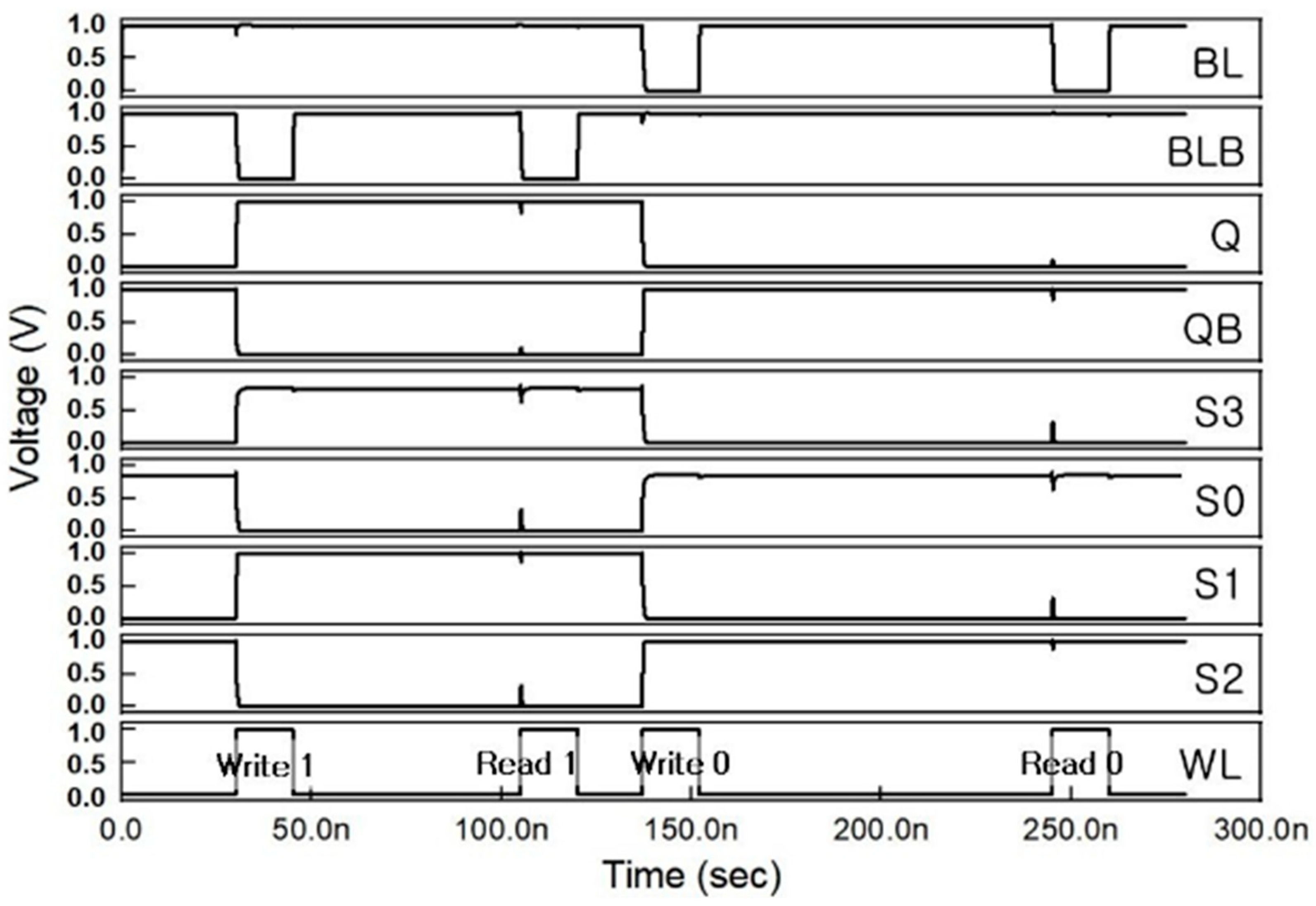
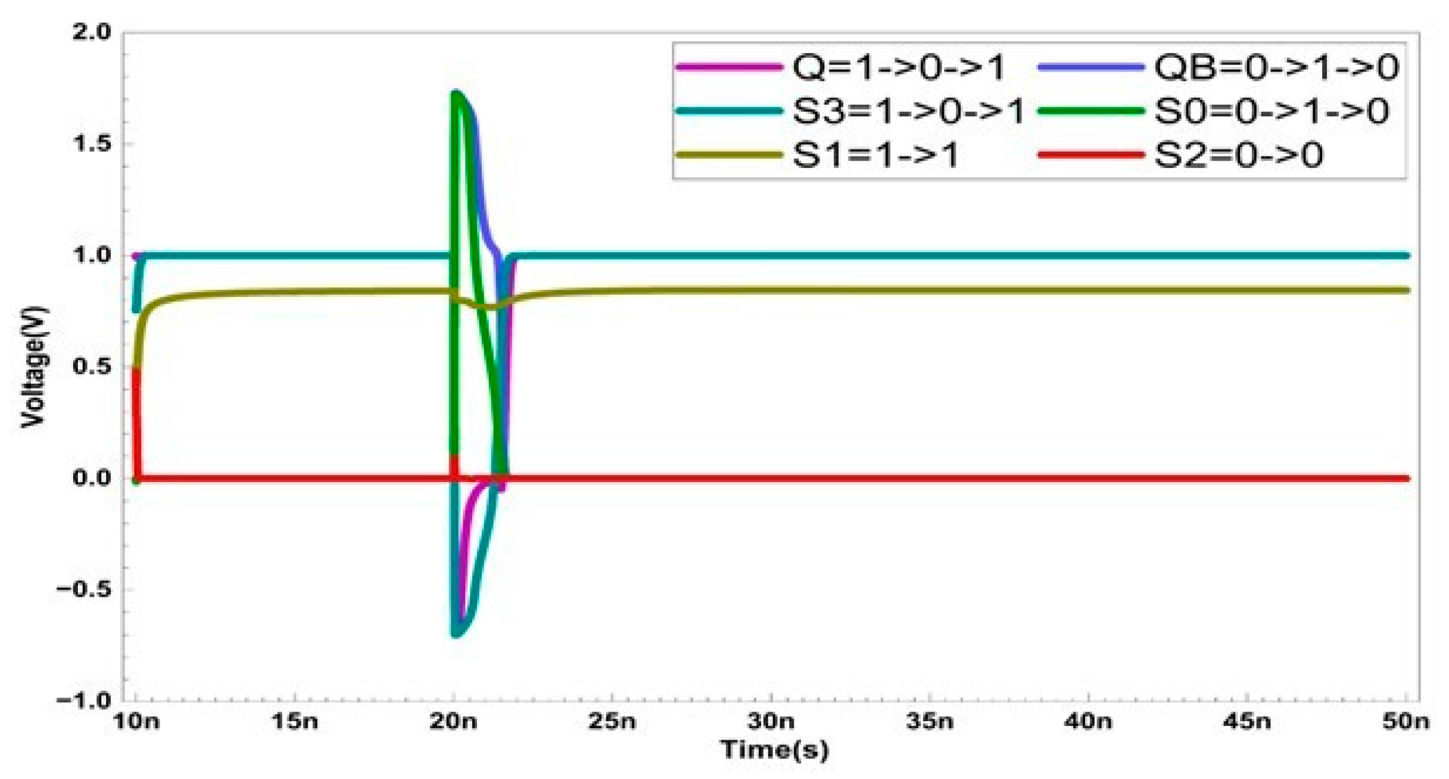
The schematic and layout of the proposed RHRSE-20T SRAM are shown in Figure 1 and Figure 2, respectively. The RHRSE-20T features two storage nodes, Q and QB, and four internal nodes, S0, S1, S2, and S3. With a total of six nodes, it is composed of 20 transistors. Transistors N4 and N5 have a width that is 2.5 times the minimum transistor width in the process, while transistors N9 and N10 have a width that is approximately 1.7 times the minimum width. The remaining transistors maintain the minimum width and length specified by the process. The widths of the transistors were determined through a series of experiments to ensure complete immunity to SNU and to enhance certain performance aspects over existing designs. The transistor widths of N4 and N5 strengthen the pull-down of the main storage node QB, ensuring that the values of Q and QB are immune to SEU. Figure 1 shows the scenario when the cell stores a ‘1’. In this state, Q = S1 = S3 = ‘1’, and QB = S0 = S2 = ‘0’. The read operation is performed through access transistors N11, N12, N13, and N14, while the write operation is carried out using a total of six access transistors, including N9 and N10. In Figure 3, it can be seen that the write, read, and hold operations of the RHRSE-20T are functioning normally.
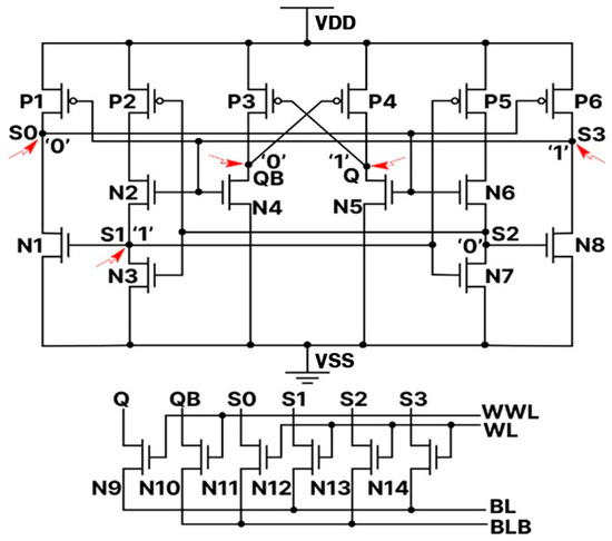
Figure 1.
Proposed RHRSE-20T SRAM schematic.

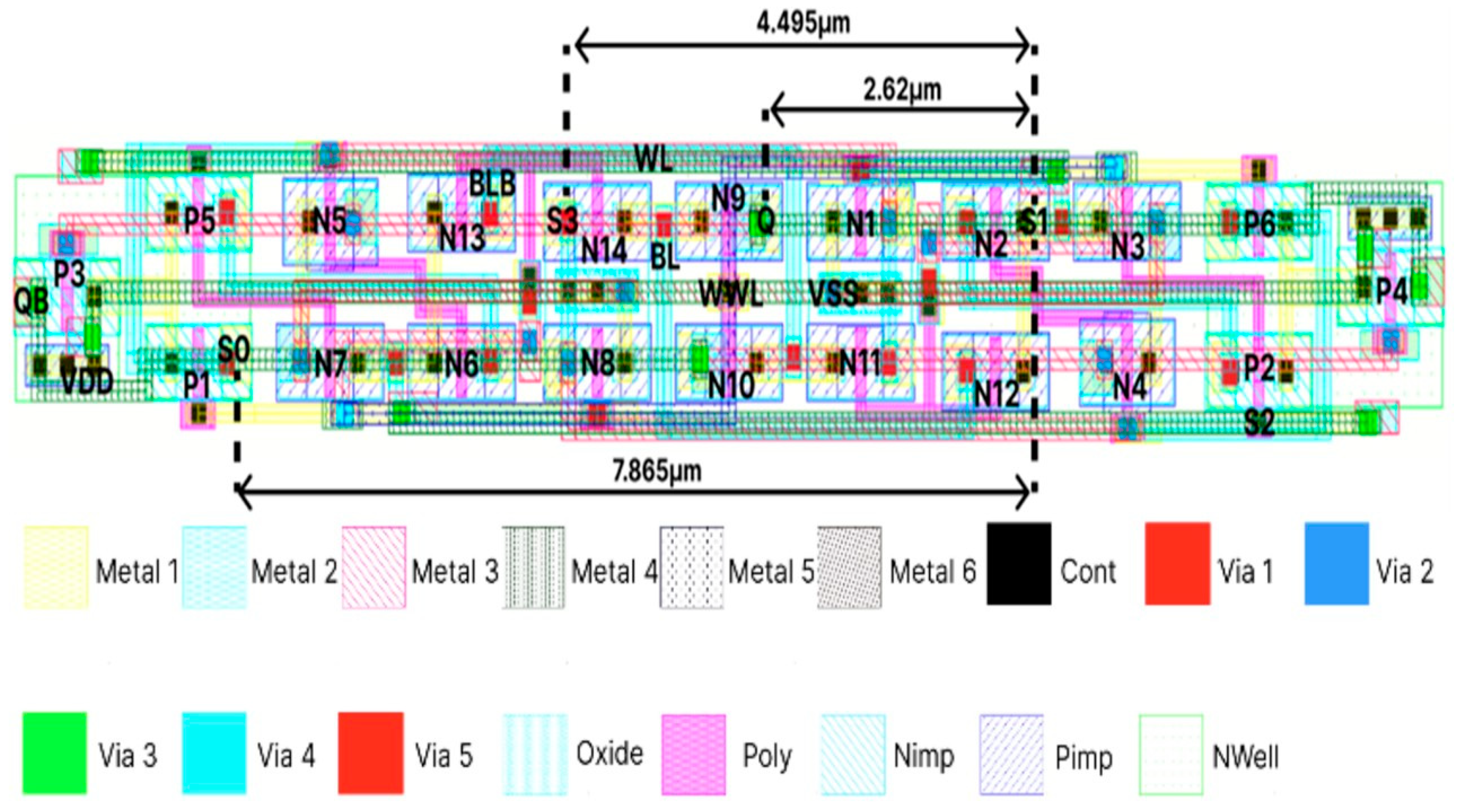
Figure 2.
Layout of RHRSE-20T SRAM.
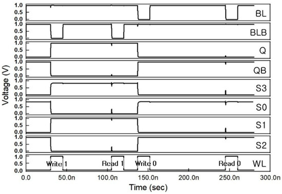
Figure 3.
Simulation results of normal write, hold, and read operations of the proposed RHRSE-20T SRAM.
2.2. Write Operation
Assume the cell is in a state where logic ‘1’ is stored (Q = S1 = S3 = 1, QB = S0 = S2 = 0). To perform a write operation for ‘0’, BL is set to ‘0’ and BLB is set to ‘1’. Both WL and WWL are driven HIGH, activating all three pairs of access transistors during the write operation. As WL and WWL transition from ‘0’ to ‘1’, the following occurs: node Q switches from ‘1’ to ‘0’ through transistor N9, node S3 switches from ‘1’ to ‘0’ through transistor N14, and node S1 switches from ‘1’ to ‘0’ through transistor N12. Simultaneously, node QB switches from ‘0’ to ‘1’ through transistor N10, node S0 switches from ‘0’ to ‘1’ through transistor N11, and node S2 switches from ‘0’ to ‘1’ through transistor N13. This completes the write operation of ‘0’ in the SRAM.
2.3. Hold Operation
Throughout the hold operation, as neither read nor write actions take place, both WL and WWL stay in a low state. The SRAM maintains the stored value through negative feedback. Assume that the data stored in the SRAM is ‘1’ (Q = S1 = S3 = 1, QB = S0 = S2 = 0), transistors P2, P4, P6, and N2 are turned on, while transistors N3, N5, and N8 are turned off to maintain the data ‘1’. Additionally, transistors N1, N4, and N7 are turned on, while transistors P1, P3, P5, and N6 are turned off, allowing the data ‘0’ to be maintained.
2.4. Read Operation
To describe the process of the read operation, assume that the SRAM is in a state where ‘0’ is stored (Q = S1 = S3 = 0, QB = S0 = S2 = 1). For the read operation, BL and BLB are pre-charged to ‘1’. Since WL and WWL are separate, WWL is not activated during the read operation. Therefore, only WL is HIGH, and the read operation utilizes only two pairs of access transistors. The access transistor connected to the node storing ‘1’ maintains the voltage of BL at the pre-charged level. In contrast, BLB, which is connected to the node storing ‘0’, will have a voltage lower than the pre-charged level. At this point, the sense amplifier detects the voltage difference between BL and BLB, and if the difference exceeds the specified threshold, it provides the output.
The following subsections provide a detailed explanation of the soft-error recovery mechanism implemented in the proposed architecture. In this section, we examine the case in which the cell stores a ‘1’ (Q = S1 = S3 = 1, QB = S0 = S2 = 0). The proposed design can recover from all SNU cases. Additionally, with the aid of layout techniques, it can recover from all DNU and MNU cases.
To simulate a radiation strike on sensitive nodes, an exponential current is applied, which can fully invert the state of the node. In such scenarios, the sensitive nodes of the cell will return to their original state through a recovery mechanism whenever data corruption occurs due to external disturbances. The self-recovery principle of the proposed RHRSE-20T cell is designed to automatically restore the cell to its original state in the event of data corruption caused by external disturbances, such as radiation.
2.5. Single Node Upset Recovery Analysis
2.5.1. Single Event Transient Occurs at Node Q
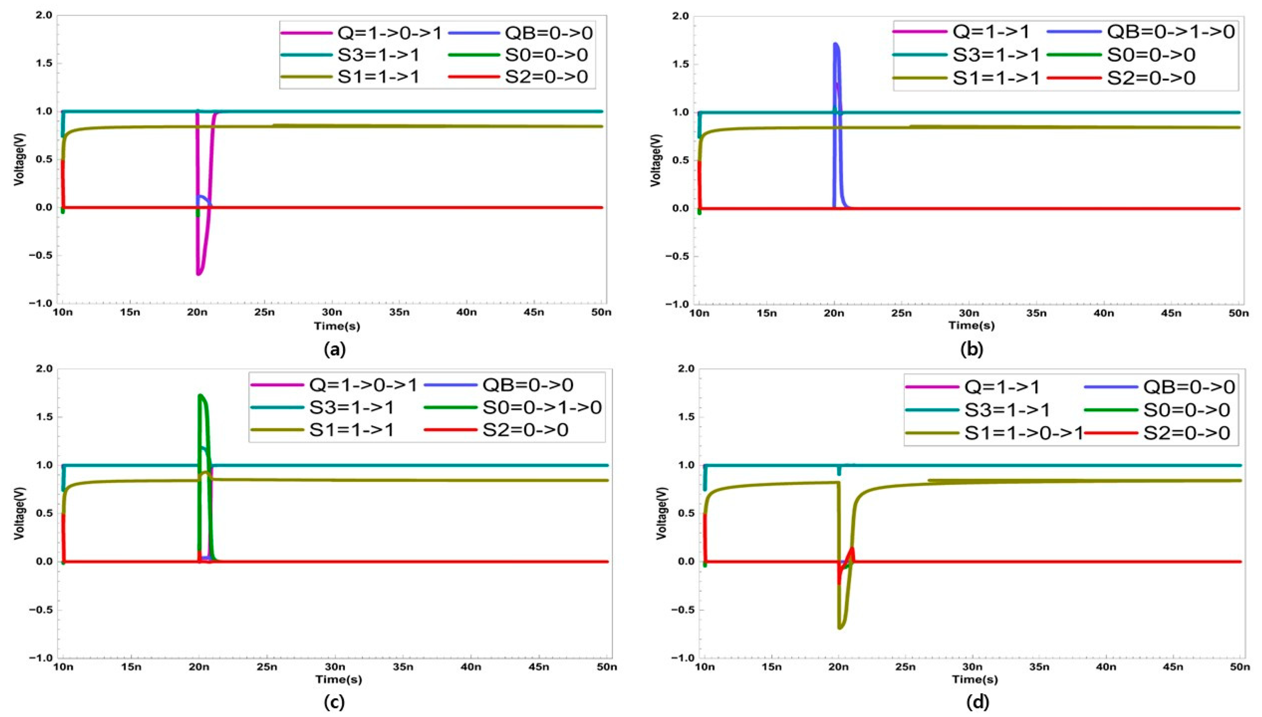
In the case of an SNU, only five sensitive nodes (Q, QB, S0, S1, S3) are considered. In Figure 4, the recovery process of the five sensitive nodes (Q, QB, S0, S1, S3) is presented. Node S2 stores a strong ‘0’, and the possibility of it being ’1’ is not considered, as it is surrounded by NMOS transistors. When a SET occurs at node Q, Q changes from ‘1’ to ‘0’. This activates transistor P3. Since the other nodes are unaffected by the SET at Q, they maintain their original values. As a result, the SEU that occurred in Q does not affect S3, and N4 remains activated. Since the width of the transistor N4 is larger, QB maintains ‘0’ despite the influence of P3. Therefore, QB activates P4. Since S0 is storing ‘0’, N5 is deactivated. Ultimately, Q is restored to ‘1’ through P4.
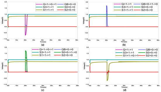
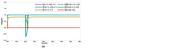
Figure 4.
Single node upset recovery when SET occurs at node (a) Q (b) QB (c) S0 (d) S1, and (e) S3.
2.5.2. Single Event Transient Occurs at Node QB
QB changes from ‘0’ to ‘1’. This deactivates transistor P4. However, the other nodes remain unaffected by the SET at QB, preserving their original values. As a result, even though transistor P4 is deactivated, Q maintains its ‘1’ state due to the activation of N5. Node S3 retains the value ‘1’, which activates transistor N4, allowing QB to recover from ‘1’ to ‘0’. Through this process, all nodes are restored to their original states.
2.5.3. Single Event Transient Occurs at Node S0
S0 changes from ‘0’ to ‘1’. This activates transistors N5 and N6, causing node Q to change from ‘1’ to ‘0’. However, nodes S1, S2, and S3 remain unaffected by the SET at S0, preserving their original values. Consequently, transistor P4 remains deactivated due to node S3, while N1 is activated by S1, allowing S0 to recover to ‘0’. As the restored S0 deactivates transistors N5 and N6, Q recovers to ‘1’. Through this process, all nodes are restored to their original states.
2.5.4. Single Event Transient Occurs at Node S1
S1 changes from ‘1’ to ‘0’. This deactivates transistor N1 and activates P5 but does not affect the values stored in the other nodes. Transistor N2 is activated by node S3, and P2 is activated by node S2 while N3 is deactivated. Consequently, S1 recovers from ‘0’ to ‘1’. Through this process, all nodes are restored to their original states.
2.5.5. Single Event Transient Occurs at Node S3
S3 changes from ‘1’ to ‘0’. This deactivates transistors N2 and N4 and activates P1. However, since node S1 firmly maintains the value ‘1’, transistor N1 also remains activated, although both P1 and N1 are temporarily activated at node S0. However, since S1 remains unchanged and continues to hold a ‘1’, transistor N1 remains continuously activated as well. This allowing S0 to recover to ‘0’. Consequently, S0 activates transistor P6, and S3 recovers to ‘1’. Through this process, all nodes are restored to their original states.
2.6. Double Node Upset Recovery Analysis
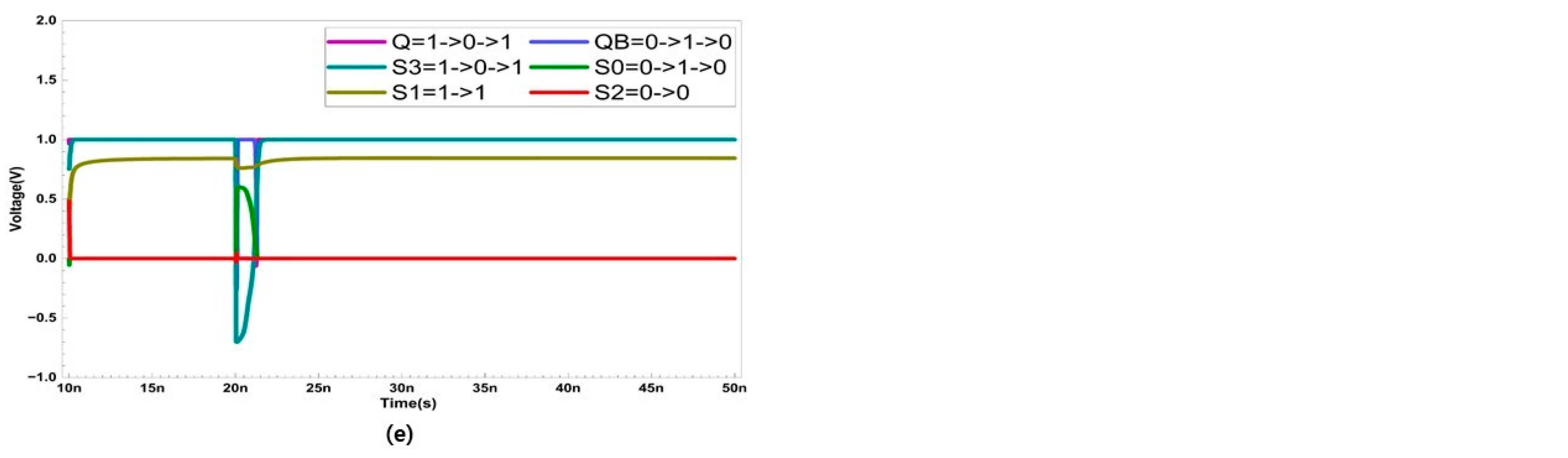
To prevent DNU, the layout is configured to separate node S1 from the other five nodes. Additionally, since S2 is an insensitive node, scenarios where S2 is struck by radiation are not considered. In Figure 5, the recovery process of all possible cases of DNU is presented.
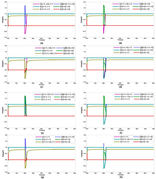
Figure 5.
Double node upset recovery when SET occurs at nodes (a) Q and QB (b) Q and S0 (c) Q and S1 (d) Q and S3 (e) S0 and QB (f) S0 and S3 (g) S1 and QB, and (h) S3 and QB.
2.6.1. Single Event Transient Occurs Simultaneously at Nodes Q and QB
Q changes from ‘1’ to ‘0’, and QB changes from ‘0’ to ‘1’. In this situation, transistor P3 is activated, and P4 is deactivated. However, the changes in Q and QB do not affect the values stored in the other nodes. Therefore, node S3 activates transistor N4, causing QB to recover to ‘0’. Consequently, node Q also recovers to ‘1’. Through this process, all nodes are restored to their original states.
2.6.2. Single Event Transient Occurs Simultaneously at Nodes Q and S0
Q changes from ‘1’ to ‘0’, and S0 changes from ‘0’ to ‘1’. This activates transistor P3, N5 and deactivates P6. However, since N4 is configured with a wider channel width than P3, node QB maintains its ‘0’ state. Except for nodes Q and S0, all other nodes retain their originally stored values. Therefore, S3 retains the value of ‘1’, which deactivates transistor P1, and S1 retains the value of ‘1’, which activates transistor N1. As a result, S0 is restored to ‘0’, deactivating transistor N5, and ultimately, Q is restored to ‘1’via P4. Through this process, all nodes are restored to their original states.
2.6.3. Single Event Transient Occurs Simultaneously at Nodes Q and S1
Q changes from ‘1’ to ‘0’, and S1 changes from ‘1’ to ‘0’. This activates transistors P3 and P5. However, these changes do not affect the other nodes, so the stored values in nodes other than Q and S1 remain unchanged. Consequently, node S2 activates transistor P2, leading to the recovery of S1 to ‘1’. Additionally, QB maintains its ‘0’ state, activating transistor P4 and allowing Q to recover to ‘1’.
2.6.4. Single Event Transient Occurs Simultaneously at Nodes Q and S3
Q changes from ‘1’ to ‘0’, and S3 changes from ‘1’ to ‘0’. This activates transistors P1 and P3. Since transistor N4 is deactivated in this scenario, QB changes to ‘1’. However, nodes S1 and S2 remain unchanged, preserving their original values. As a result, transistor N1 remains firmly activated, keeping S0 at ‘0’. Consequently, transistor P6 is activated, allowing S3 to recover to ‘1’. The recovered S3 then activates transistor N4, leading to the recovery of QB to ‘0’, and ultimately, Q also recovers to ‘1’. Through this process, all nodes are restored to their original states.
2.6.5. Single Event Transient Occurs Simultaneously at Nodes QB and S0
QB changes from ‘0’ to ‘1’, and S0 changes from ‘0’ to ‘1’. However, these changes do not affect the values stored in the other nodes. As a result, node S3 maintains its ‘1’ state, activating transistor N4, which in turn restores QB to ‘0’. Additionally, node S1 retains its ‘1’ state, activating transistor N1 and restoring S0 to ‘0’. Through this process, all nodes are restored to their original states.
2.6.6. Single Event Transient Occurs Simultaneously at Nodes QB and S1
QB changes from ‘0’ to ‘1’, and S1 changes from ‘1’ to ‘0’. This activates transistor P5 but does not affect the values stored in the other nodes. Since node S2 maintains its ‘0’ state, transistor P2 is activated, and S3 also activates N2. Consequently, S1 is restored to ‘1’. Simultaneously, S3 activates N4, which restores QB to ‘0’. Through this process, all nodes are restored to their original states.
2.6.7. Single Event Transient Occurs Simultaneously at Nodes QB and S3
QB changes from ‘0’ to ‘1’, and S3 changes from ‘1’ to ‘0’. This activates transistor P1. However, the stored values in the other nodes remain unchanged. Node S1 maintains its ‘1’ state, ensuring the strong activation of transistor N1, which keeps S0 at ‘0’. Node S0 then activates transistor P6, leading to the recovery of S3 to ‘1’. The recovered S3 activates transistor N4, which restores QB to ‘0’. Through this process, all nodes are restored to their original states.
2.6.8. Single Event Transient Occurs Simultaneously at Nodes S0 and S3
S0 changes from ‘0’ to ‘1’, and S3 changes from ‘1’ to ‘0’. This activates transistor P1 and deactivates P6. These changes in node values do not affect the values stored in the other nodes, even though transistor P1 is temporarily activated. However, since S1 remains unchanged and continues to hold a ‘1’, transistor N1 remains continuously activated as well. This leads to the recovery of S0 to ‘0’. This activation also triggers transistor P6, ultimately restoring S3 to ‘1’. Through this process, all nodes are restored to their original states.
2.7. Multiple Node Upset Recovery Analysis
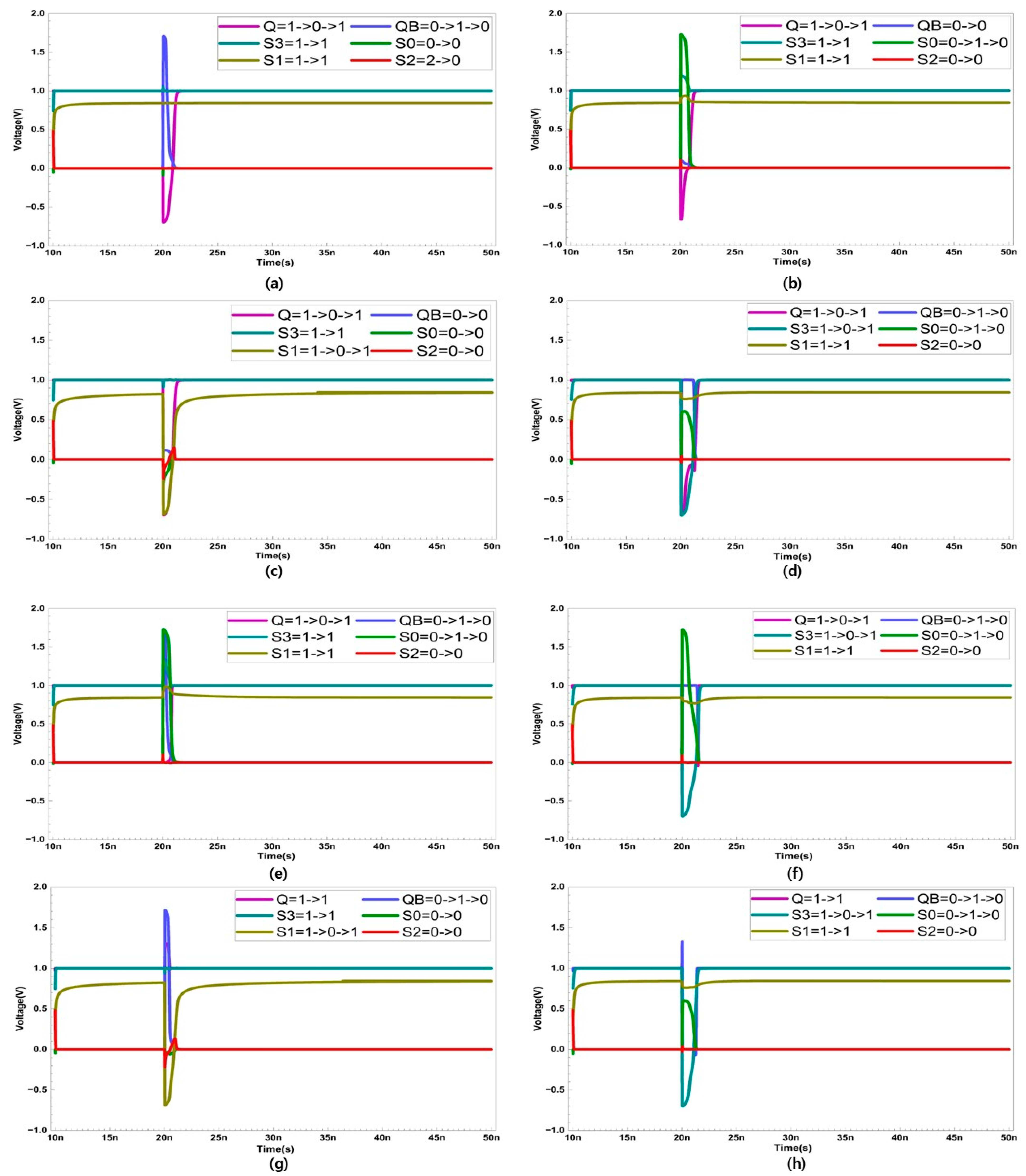
Single Event Transient Occurs Simultaneously at Nodes Q, QB, S0, and S3
The recovery process for all potential cases of MNU is presented in Figure 6. Due to the layout technique that isolates node S1 from the other nodes, MNU only considers scenarios where Q, QB, S0, and S3 are simultaneously affected by radiation.
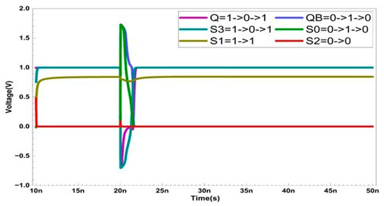
Figure 6.
Multiple node upset recovery when SET occurs at nodes Q, QB, S0, and S3.
When SETs occur simultaneously at nodes Q, QB, S0, and S3, Q changes from ‘1’ to ‘0’, QB from ‘0’ to ‘1’, S0 from ‘0’ to ‘1’, and S3 from ‘1’ to ‘0’. This situation activates transistors P3, P1, and N5. However, these changes do not affect the values stored in S1 and S2. Because node S1 firmly maintains its ‘1’ state and activates transistor N1, even if P1 is temporarily activated by radiation, S0 is restored to ‘0’. The recovered S0 then activates transistor P6, restoring S3 to ‘1’. The restored S3 subsequently activates transistor N4. Since N4 has a wider channel width than P3, even with P3 being activated, QB is restored to ‘0’. Consequently, QB activates transistor P4, and Q is also restored to ‘1’, ensuring that all nodes recover to their original states.
3. Simulation Results and Analysis
The performance of the proposed SRAM is assessed using various metrics, including read static noise margin, read and write access time, word line write trip voltage, hold power, and area. Additionally, the performance is compared with other existing designs measured under the same conditions. The performance metrics were calculated under a VDD = 1 V and 90-nm CMOS process.
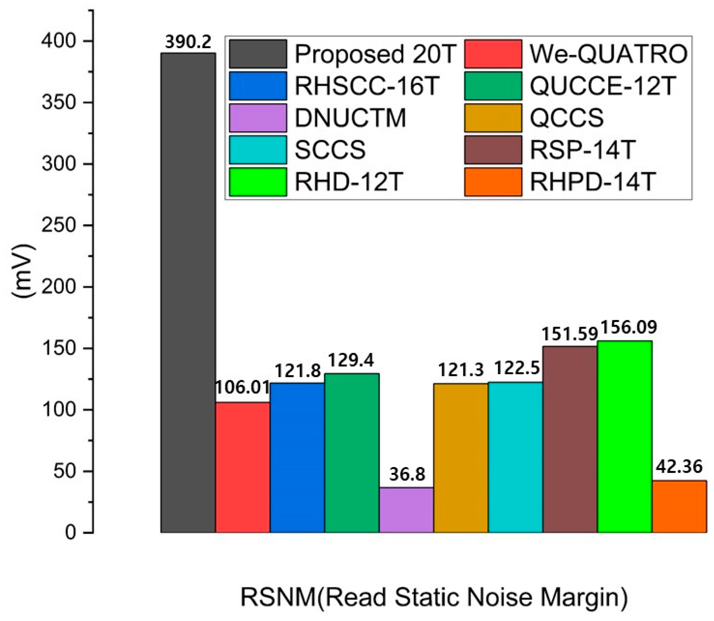
3.1. Read Static Noise Margin
During a read operation, the node storing a ‘0’ is connected to the pre-charged bit line at VDD, allowing the read current to flow. This current can cause a voltage change at the node storing the ‘0’, potentially altering the stored data. Therefore, read stability is a critical factor in SRAM design and is evaluated using the read static noise margin (RSNM). The RSNM is measured by applying a DC voltage sweep from 0 V to VDD to the main storage node and performing DC analysis to generate butterfly curves for the two main storage nodes. The RSNM is then derived from the largest square area that can be inserted within the butterfly curves measured at each storage node during the read operation [14]. RSNM is a critical parameter in SRAM design as it quantifies the cell’s ability to maintain data integrity during read operations. A higher RSNM indicates improved resistance to soft errors, thereby enhancing the reliability of memory devices in radiation-prone environments. Consequently, optimizing RSNM is essential for ensuring stable performance in advanced semiconductor applications.
The RHRSE-20T design separates the word line (WL) and the write word line (WWL), utilizing only two pairs of access transistors during the read operation. The use of more access transistors can degrade both read and write stability due to parasitic capacitance. Consequently, the RSNM of the RHRSE-20T is more than three times larger than that of the SCCS, which uses more than two pairs of access transistors, and more than ten times larger than that of the DNUCTM. Furthermore, the width (W) of transistors N4 and N5 is set to 300 nm, resulting in a higher cell ratio (CR) compared to other reference cells, thereby enhancing RSNM performance. The impact of CR on parasitic capacitance and area cost is critical in determining the stability and performance of SRAM cells. A higher CR typically necessitates larger transistors, which leads to an increase in area cost. However, larger transistors reduce parasitic capacitance due to their improved ability to handle larger currents, thus enhancing noise margins and improving stability. In this design, the transistor width was optimized to achieve a balance between improved stability (RSNM) and minimized parasitic capacitance, ultimately enhancing both read and write operations. Nevertheless, the increase in transistor size associated with a higher CR result in a trade-off as it increases the overall area cost. While the larger CR in the RHRSE-20T design improves the RSNM and mitigates the effects of parasitic capacitance, it also requires more chip area compared to designs with a lower CR. The RSNM of various SRAM designs is compared in Figure 7, confirming that the proposed RHRSE-20T exhibits the best RSNM performance.

Figure 7.
Comparison results of the read static noise margin of the proposed RHRSE-20T with previous works.
3.2. Read Access Time
Read access time (RAT) is crucial in SRAM design as it directly affects the speed at which data can be retrieved from memory. A faster RAT leads to improved overall system performance, particularly in high-speed applications where timely data access is essential. RAT is measured as the time interval from when the word line voltage reaches 50% of VDD to when a 50 mV voltage difference is established between BL and BLB. This occurs during the read operation due to the voltage drop on the bit line through the access transistor and the pull-down transistor. Therefore, an SRAM cell with a high CR generally has a lower RAT. However, the absolute number of access transistors does not necessarily reduce the RAT. As the number of access transistors connected to the bit line increases, parasitic capacitance also increases, which can lead to a higher RAT [15]. Thus, although the RHSCC-16T uses three pairs of access transistors, it has a longer RAT due to increased parasitic capacitance. The proposed SRAM uses only two access transistors but achieves the best RAT among the compared cells due to an optimal CR (node Q = 1.5) and a moderate number of access transistors. These results demonstrate the efficiency of the proposed design, particularly in applications where fast read times are critical. The RAT values of all comparison cells are shown in Figure 8.
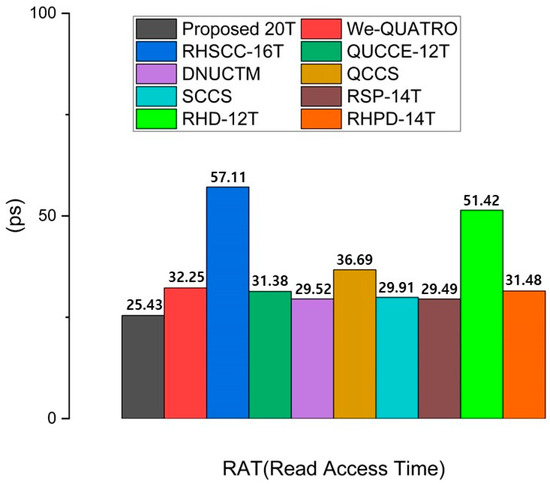
Figure 8.
Comparison results of the read access time of the proposed RHRSE-20T with previous works.
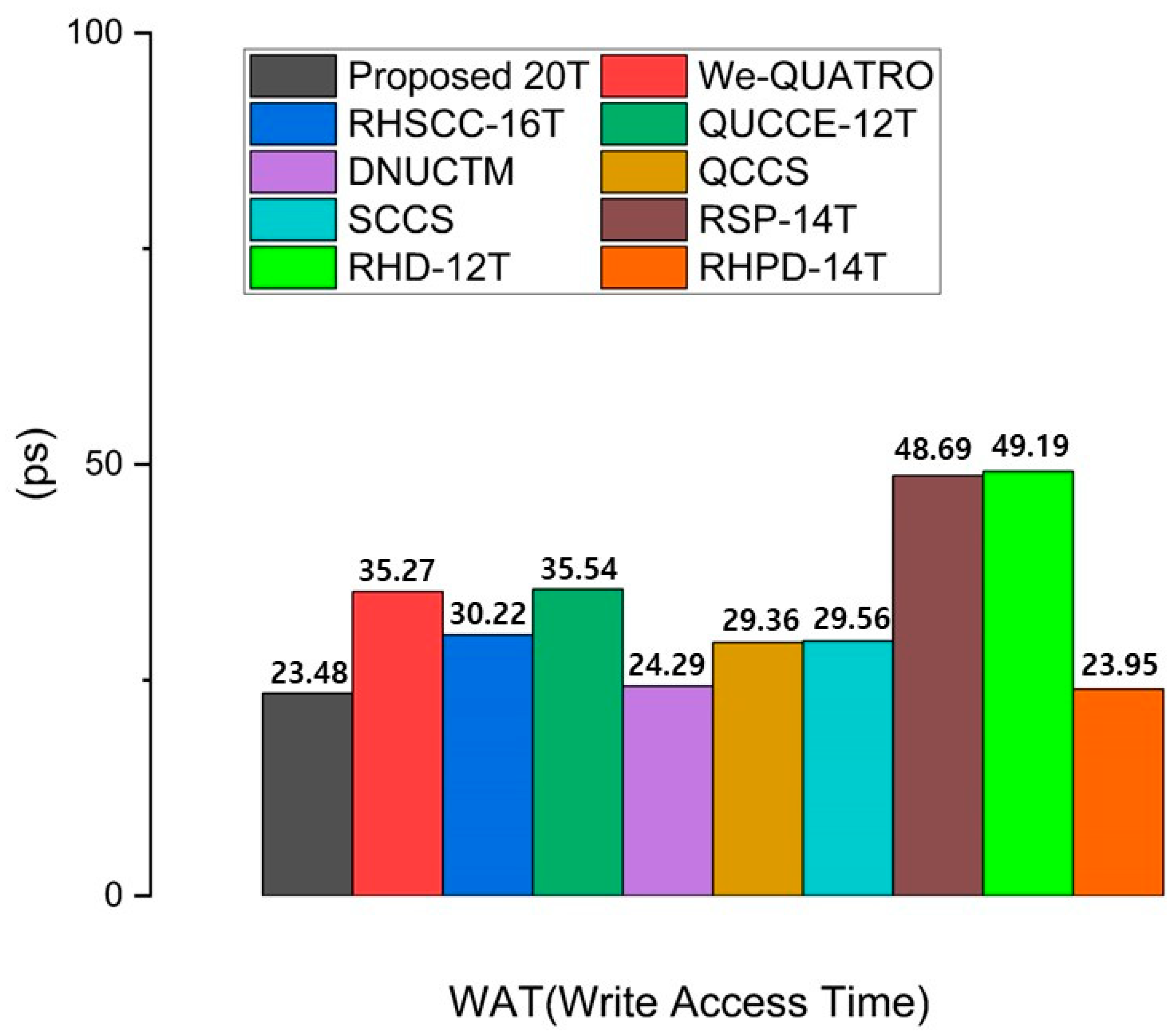
3.3. Write Access Time
Write access time (WAT) is important in SRAM design because it determines how quickly data can be written to memory cells. A shorter WAT enables faster updates and modifications, which is essential for applications requiring real-time data processing. Write access time (WAT) is defined as the time interval between when the word line reaches 50% of VDD and when the voltages at the storage nodes Q and QB intersect. Figure 9 shows that using more access transistors typically reduces WAT. However, despite using four pairs of access transistors, DNUCTM has a higher WAT compared to the proposed circuit. This is because the proposed RHRSE-20T allows the S1 node to store a weak ‘1’, enabling faster write times than DNUCTM. Additionally, without any additional paths for write operations, the proposed design uses three pairs of access transistors to directly perform write operations on two storage nodes and four internal nodes, resulting in the lowest WAT. This makes it highly suitable for applications requiring fast write performance. The WAT values of all comparison cells are presented in Figure 9.
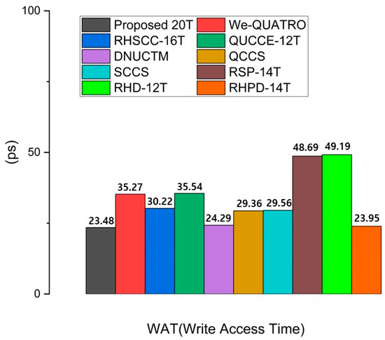
Figure 9.
Comparison results of the write access time of the proposed RHRSE-20T with previous works.
3.4. Word Line Write Trip Voltage
Word line write trip voltage (WWTV) is crucial in SRAM design as it influences the reliability and stability of write operations. A well-defined WWTV ensures that the correct voltage is applied to trigger the writing of data, reducing the risk of accidental data corruption. WWTV is defined as the voltage difference between VDD and the word line voltage at the intersection of the voltages at nodes Q and QB during a write operation. The proposed RHRSE-20T uses a total of three pairs of access transistors during the write operation, enhancing the SRAM’s write performance. In Figure 10, the WWTV values of all comparison cells are presented. As a result, it achieves the best WWTV among the compared cells.
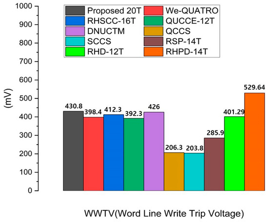
Figure 10.
Comparison results of the word line trip voltage of the proposed RHRSE-20T with previous works.
3.5. Hold Power
Hold power (HPWR) is important in SRAM design because it represents the power consumed when the memory cells are in a stable state and not actively reading or writing. The measurement method for HPWR in SRAM consists of two components: one through leakage power via the pull-up and pull-down paths and the other through the bit-line. To measure these, a pulse is applied to all nodes storing a ‘1’, ranging from 0 to VDD, and power is measured when VDD is reached. HPWR dissipation occurs due to leakage in the bit lines and within the SRAM’s internal structure. In bit lines, NMOS transistors, with their higher carrier mobility, exhibit greater HPWR compared to PMOS transistors. Within the internal structure, the more paths from VDD to the ground, the higher the HPWR. The proposed design, which uses three pairs of NMOS access transistors and has the highest number of paths (six) from VDD to the ground, exhibits the highest HPWR among the compared cells. However, in designing a radiation-hardened SRAM, more emphasis is placed on the robustness of the design against radiation strikes and the stability of the cells. Due to its superior radiation resistance compared to conventional designs, the proposed design is more suitable for radiation-hardened applications. The HPWR values of all comparison cells are presented in Figure 11.
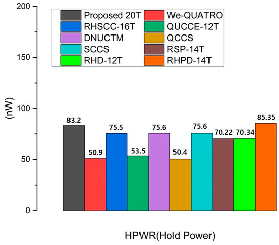
Figure 11.
Comparison results of the hold power of the proposed RHRSE-20T with previous works.
3.6. Area
A specific layout technique was employed to ensure recovery from all possible cases of DNU and MNU. In a DNU, if sufficient charge is injected at nodes (S1-S0) and (S1-S3), the stored value may flip. Therefore, the drains of the NMOS and PMOS transistors that could cause an SNU were separated by at least 1.62 μm [16,17]. Due to this arrangement, the proposed cell is resistant to all potential cases of soft errors. Of the 20 transistors used, 16 are sized at the minimum dimensions allowed by the fabrication process. However, due to the use of the largest number of transistors among the compared cells, the proposed design has the largest area, measuring 28.28 μm2.
3.7. Soft Error Robustness Analyses
To evaluate the robustness of the proposed cell against single event transient (SET) or soft errors, we examined its tolerance to soft errors by introducing a current source into the vulnerable nodes. The double exponential current is expressed as follows:
The constants and represent the time constants for the initial ion track formation and are set to 200 ps and 50 ps, respectively [7,18]. The robustness of the SRAM is measured by the critical charge (Qc). Qc refers to the minimum amount of charge required to flip the stored value in the cell when a sensitive node is affected by an SET. It is measured based on the node with the smallest Qc among the various nodes in the SRAM. Qc is expressed as follows, where denotes the time at which the cell’s stored value is flipped.
The Qc values of the existing and proposed SRAM cells are listed in Table 1. Cells where the value of the storage node did not flip within the measurement range are marked with a Qc of 300 or higher. Except for RHSCC-16T and DNUCTM, the remaining cells have finite Qc values because they are not fully immune to SNU or DNU. The proposed cell is immune to all cases of SNU and, in conjunction with layout techniques, is also immune to all possible cases of DNU and MNU. Therefore, it is highly suitable for environments exposed to radiation.

Table 1.
Critical charge comparisons for SNU.
4. Conclusions
In this paper, a radiation hardened read-stability and speed enhanced 20T (RHRSE-20T) SRAM is proposed for environments prone to radiation exposure. The RHRSE-20T SRAM demonstrates a read static noise margin (RSNM) that is improved by 255% compared to the average of conventional cells, along with a word line trip voltage (WWTV) that shows a 19% improvement. Additionally, read delays are reduced by 30% compared to conventional SRAM cells, significantly enhancing overall performance. Furthermore, the design shows immunity to potential soft errors, achieved for SEU, DNU, and MNU, thus providing superior radiation resistance. These advancements make the proposed RHRSE-20T SRAM particularly well-suited for terrestrial, atmospheric, and space applications, where reliability in harsh conditions is essential.
Author Contributions
Conceptualization, W.C.C. and S.-H.J.; methodology, W.C.C.; validation, W.C.C.; data curation, W.C.C.; writing—original draft preparation, W.C.C.; writing—review and editing, S.-H.J.; visualization, W.C.C.; supervision, S.-H.J.; project administration, S.-H.J. All authors have read and agreed to the published version of the manuscript.
Funding
This research received no external funding.
Institutional Review Board Statement
Not applicable.
Informed Consent Statement
Not applicable.
Data Availability Statement
Data are contained within the article.
Acknowledgments
The EDA Tool was supported by the IC Design Education Center, Korea.
Conflicts of Interest
The authors declare no conflicts of interest.
References
- International Roadmap for Devices and Systems. 2023 IRDS Perspectives. Institute of Electrical and Electronics Engineers. 2023. Available online: https://irds.ieee.org/editions/2023 (accessed on 25 September 2024).
- Hashimoto, M.; Kobayashi, K.; Furuta, J.; Abe, S.-I.; Watanabe, Y. Characterizing SRAM and FF soft error rates with measurement and simulation. Integration 2019, 69, 161–179. [Google Scholar] [CrossRef]
- Watkins, A.; Tragoudas, S. Radiation hardened latch designs for double and triple node upsets. IEEE Trans. Emerg. Top. Comput. 2017, 8, 616–626. [Google Scholar] [CrossRef]
- Rajaei, R.; Asgari, B.; Tabandeh, M.; Fazeli, M. Single event multiple upset-tolerant SRAM cell designs for nano-scale CMOS technology. Turk. J. Electr. Eng. Comput. Sci. 2017, 25, 1035–1047. [Google Scholar] [CrossRef]
- Guo, J.; Liu, S.; Zhu, L.; Lombardi, F. Design and Evaluation of Low-Complexity Radiation Hardened CMOS Latch for Double-Node Upset Tolerance. IEEE Trans. Circuits Syst. Regul. Pap. 2020, 67, 1925–1935. [Google Scholar] [CrossRef]
- Dang, L.D.T.; Kim, J.S.; Chang, I.J. We-quatro: Radiation-hardened SRAM cell with parametric process variation tolerance. IEEE Trans. Nucl. Sci. 2017, 64, 2489–2496. [Google Scholar] [CrossRef]
- Bharti, P.K.; Mekie, J. RHSCC-16T: Radiation Hardened sextuple cross coupled robust SRAM Design for Radiation prone environments. In Proceedings of the 2022 IEEE 40th International Conference on Computer Design (ICCD), IEEE, Olympic Valley, CA, USA, 23–26 October 2022. [Google Scholar] [CrossRef]
- Jiang, J.; Xu, Y.; Zhu, W.; Xiao, J.; Zou, S. Quadruple cross-coupled latch-based 10T and 12T SRAM bit-cell designs for highly reliable terrestrial applications. IEEE Trans. Circuits Syst. I Regul. Pap. 2019, 66, 967–977. [Google Scholar] [CrossRef]
- Yan, A.; Wu, Z.; Guo, J.; Song, J.; Wen, X. Novel double-node-upset-tolerant memory cell designs through radiation-hardening-by-design and layout. IEEE Trans. Reliab. 2019, 68, 354–363. [Google Scholar] [CrossRef]
- Yan, A.; Xiang, J.; Cao, A.; He, Z.; Cui, J.; Ni, T.; Huang, Z.; Wen, X.; Girard, P. Quadruple and sextuple cross-coupled SRAM cell designs with optimized overhead for reliable applications. IEEE Trans. Device Mater. Reliab. 2022, 22, 282–295. [Google Scholar] [CrossRef]
- Peng, C.; Huang, J.; Liu, C.; Zhao, Q.; Xiao, S.; Wu, X.; Lin, Z.; Chen, J.; Zeng, X. Radiation-hardened 14T SRAM bitcell with speed and power optimized for space application. IEEE Trans. Very Large Scale Integr. (VLSI) Syst. 2018, 27, 407–415. [Google Scholar] [CrossRef]
- Qi, C.; Xiao, L.; Wang, T.; Li, J.; Li, L. A highly reliable memory cell design combined with layout-level approach to tolerant single-event upsets. IEEE Trans. Device Mater. Reliab. 2016, 16, 388–395. [Google Scholar] [CrossRef]
- Hao, L.; Qiang, B.; Dai, C.; Peng, C.; Lu, W.; Lin, Z.; Liu, L.; Zhao, Q.; Wu, X.; Sun, F. Radiation-hardened 14T SRAM cell by polar design for space applications. IEICE Electron. Express 2023, 20, 20230083. [Google Scholar] [CrossRef]
- Seevinck, E.; List, F.; Lohstroh, J. Static-noise margin analysis of MOS SRAM cells. IEEE J. Solid-State Circuits 1987, 22, 748–754. [Google Scholar] [CrossRef]
- Sheu, M.-H.; Morsalin, S.M.S.; Tsai, C.-M.; Yang, C.-J.; Hsia, S.-C.; Hsueh, Y.-H.; Lin, J.-F.; Chang, C.-Y. Stable Local bit-line 6 T SRAM architecture design for low-voltage operation and access enhancement. Electronics 2021, 10, 685. [Google Scholar] [CrossRef]
- Pal, S.; Mohapatra, S.; Ki, W.-H.; Islam, A. Soft-error-immune read-stability-improved SRAM for multi-node upset tolerance in space applications. IEEE Trans. Circuits Syst. I Regul. Pap. 2021, 68, 3317–3327. [Google Scholar] [CrossRef]
- Pal, S.; Sri, D.D.; Ki, W.-H.; Islam, A. Soft-error resilient read decoupled SRAM with multi-node upset recovery for space applications. IEEE Trans. Electron Devices 2021, 68, 2246–2254. [Google Scholar] [CrossRef]
- Pal, S.; Mohapatra, S.; Ki, W.-H.; Islam, A. Design of soft-error-aware SRAM with multi-node upset recovery for aerospace applications. IEEE Trans. Circuits Syst. I Regul. Pap. 2021, 68, 2470–2480. [Google Scholar] [CrossRef]


Disclaimer/Publisher’s Note: The statements, opinions and data contained in all publications are solely those of the individual author(s) and contributor(s) and not of MDPI and/or the editor(s). MDPI and/or the editor(s) disclaim responsibility for any injury to people or property resulting from any ideas, methods, instructions or products referred to in the content. |
© 2024 by the authors. Licensee MDPI, Basel, Switzerland. This article is an open access article distributed under the terms and conditions of the Creative Commons Attribution (CC BY) license (https://creativecommons.org/licenses/by/4.0/).