
Analysis and Optimization of Output Low-Pass Filter for Current-Source Single-Phase Grid-Connected PV Inverters


Abstract
1. Introduction
Design Criteria
- From 20% to the rated output power, the power factor should be 0.8 leading and 0.95 lagging;
- It is essential to minimize high-frequency harmonics, ensuring that the output current maintains a THD of less than 5%.
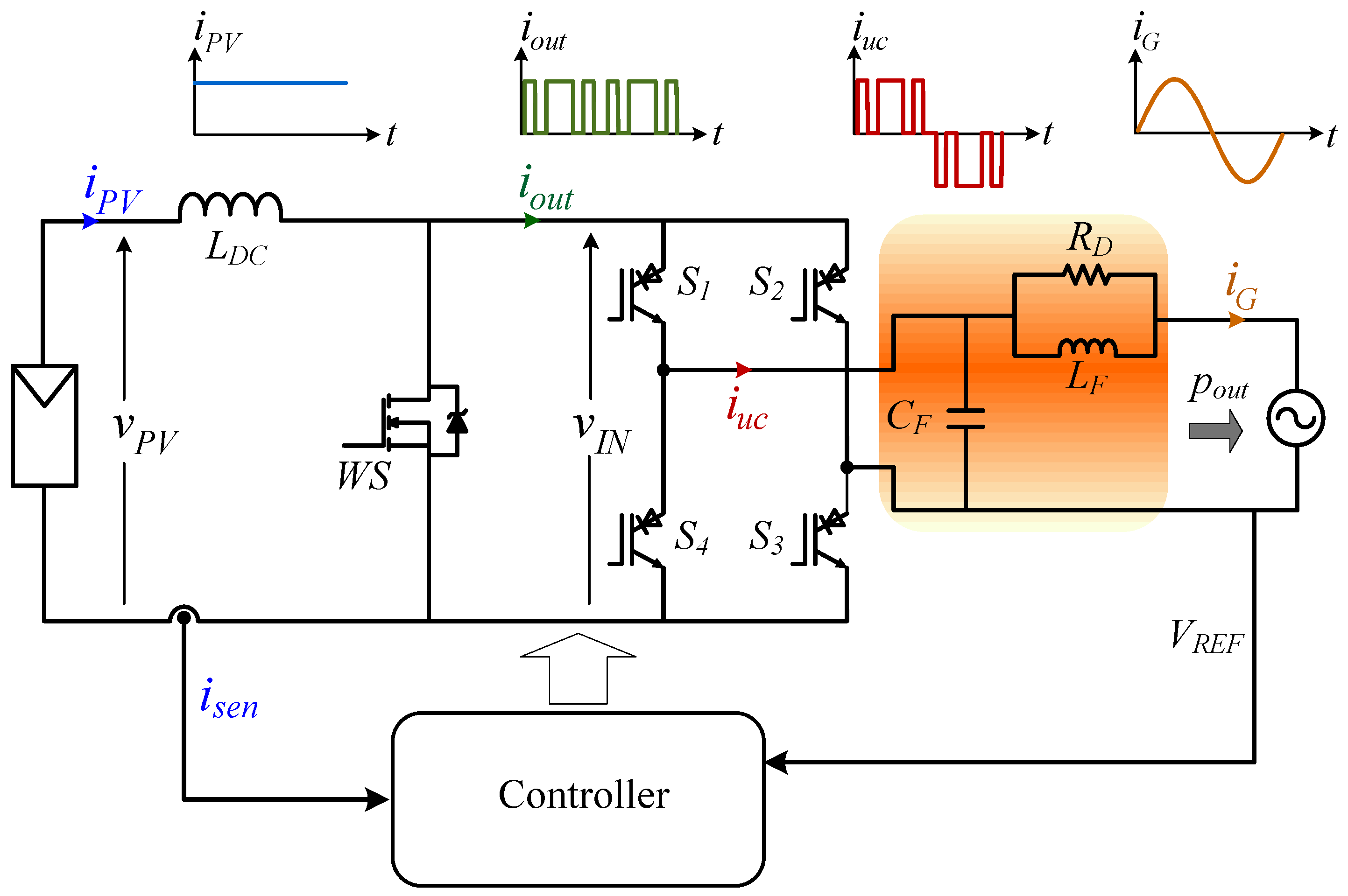
2. Filter Resonance and Damping
2.1. Filter Damping
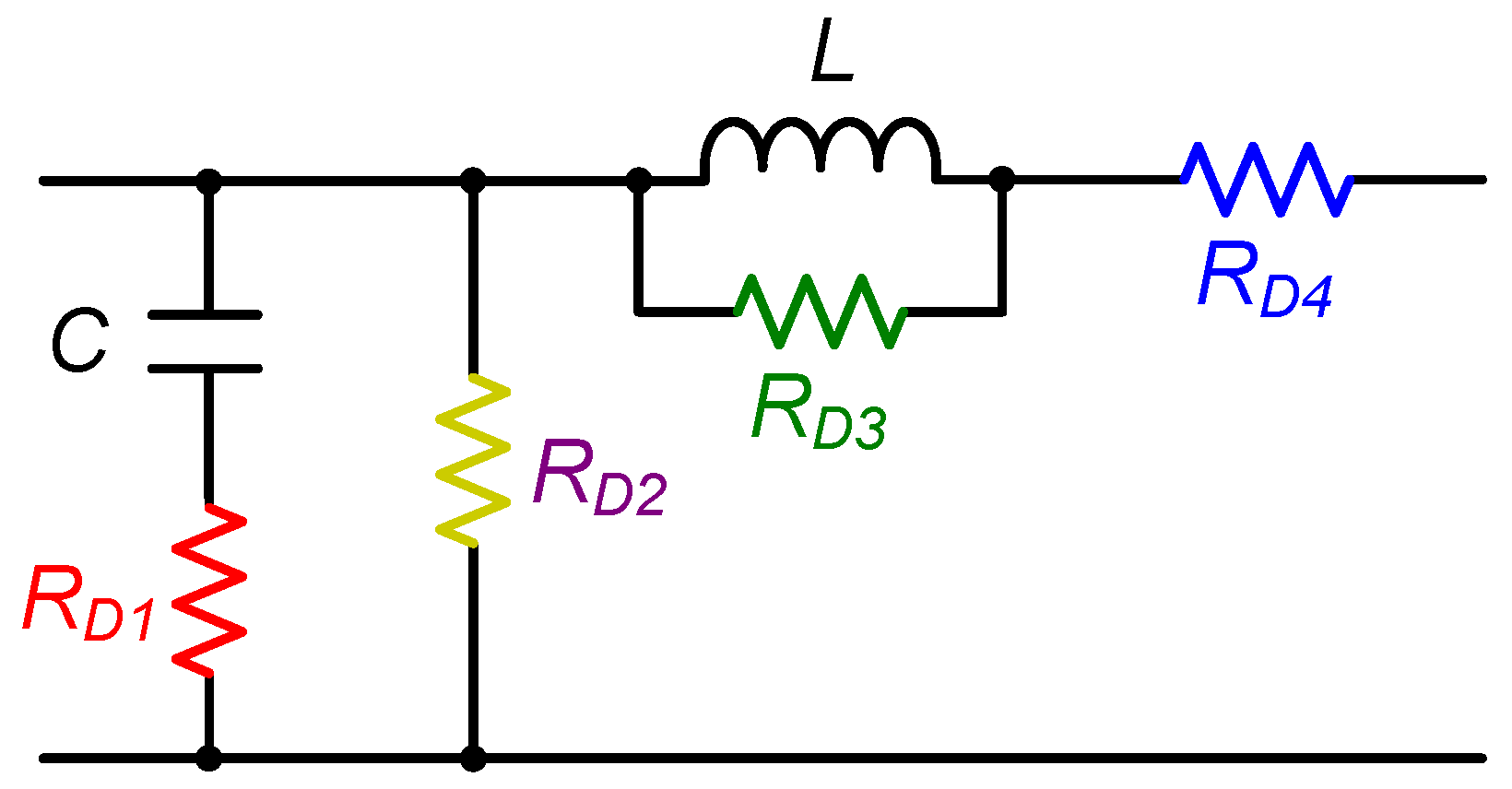
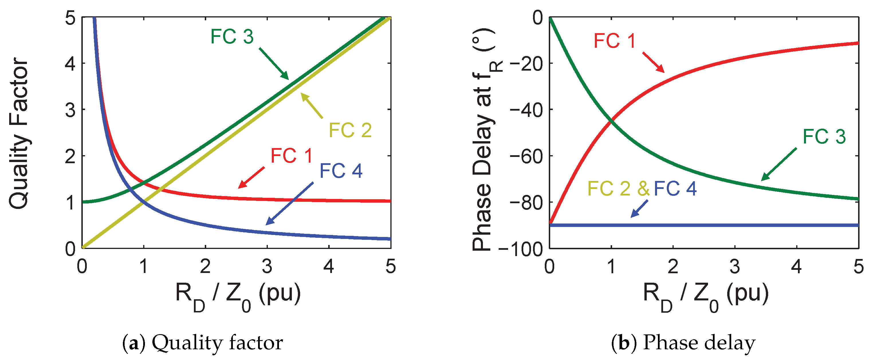
2.2. Damped Filter Response and Configuration Comparison
2.3. Filter Variables
3. Frequency and Filter Component Normalization
3.1. Practical Limits
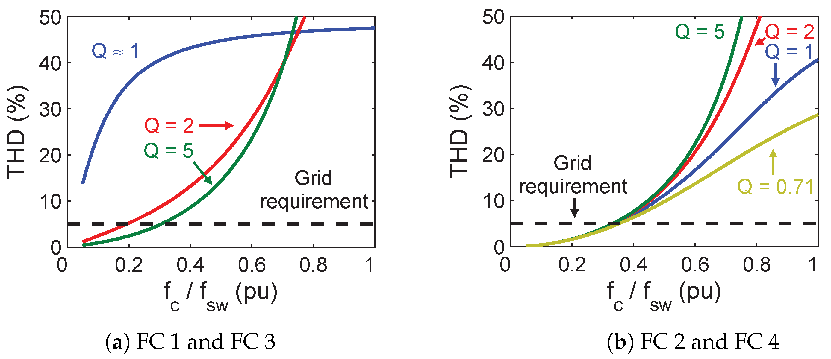
3.2. Harmonic Distortion and Attenuation
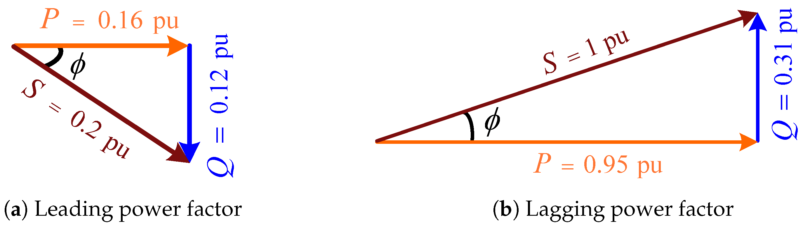
3.3. Power Factor Requirements
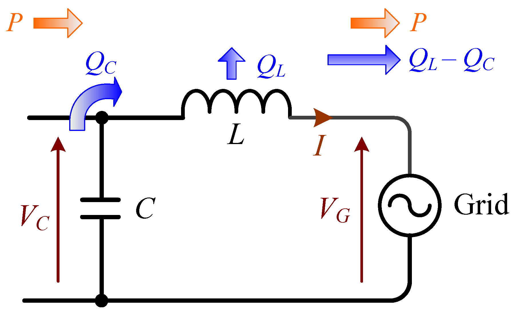
Reactive Power
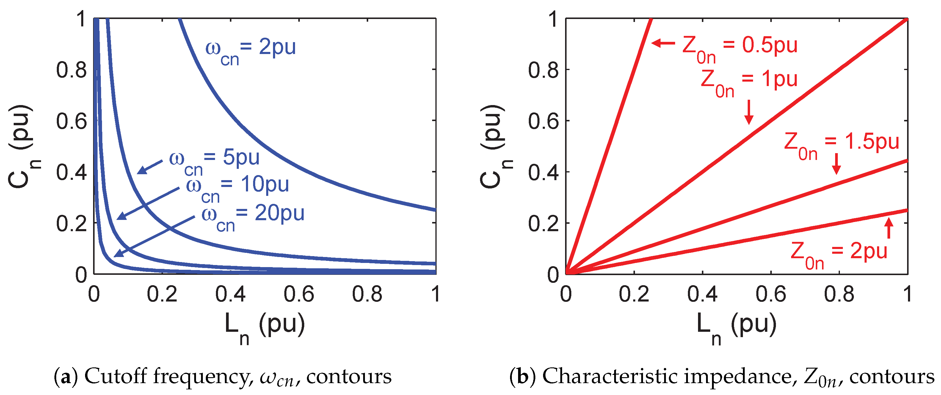
3.4. Limits of Filter Components
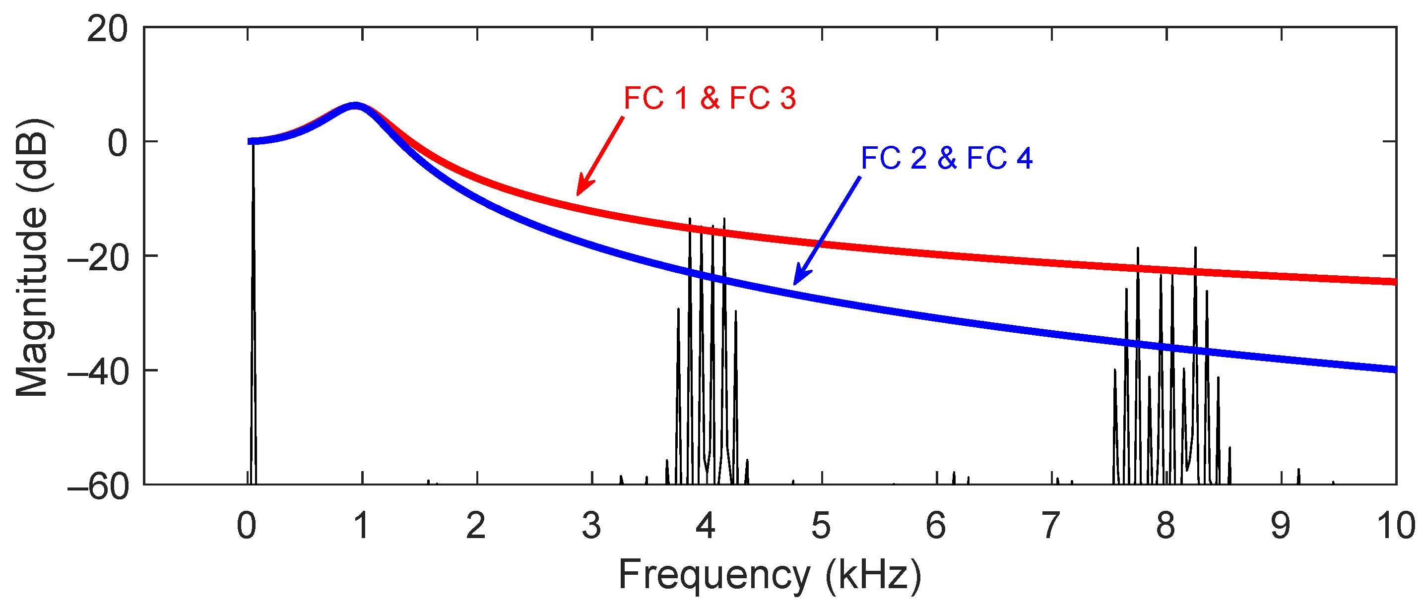
3.5. Filter Configurations
4. Design Trade-Offs
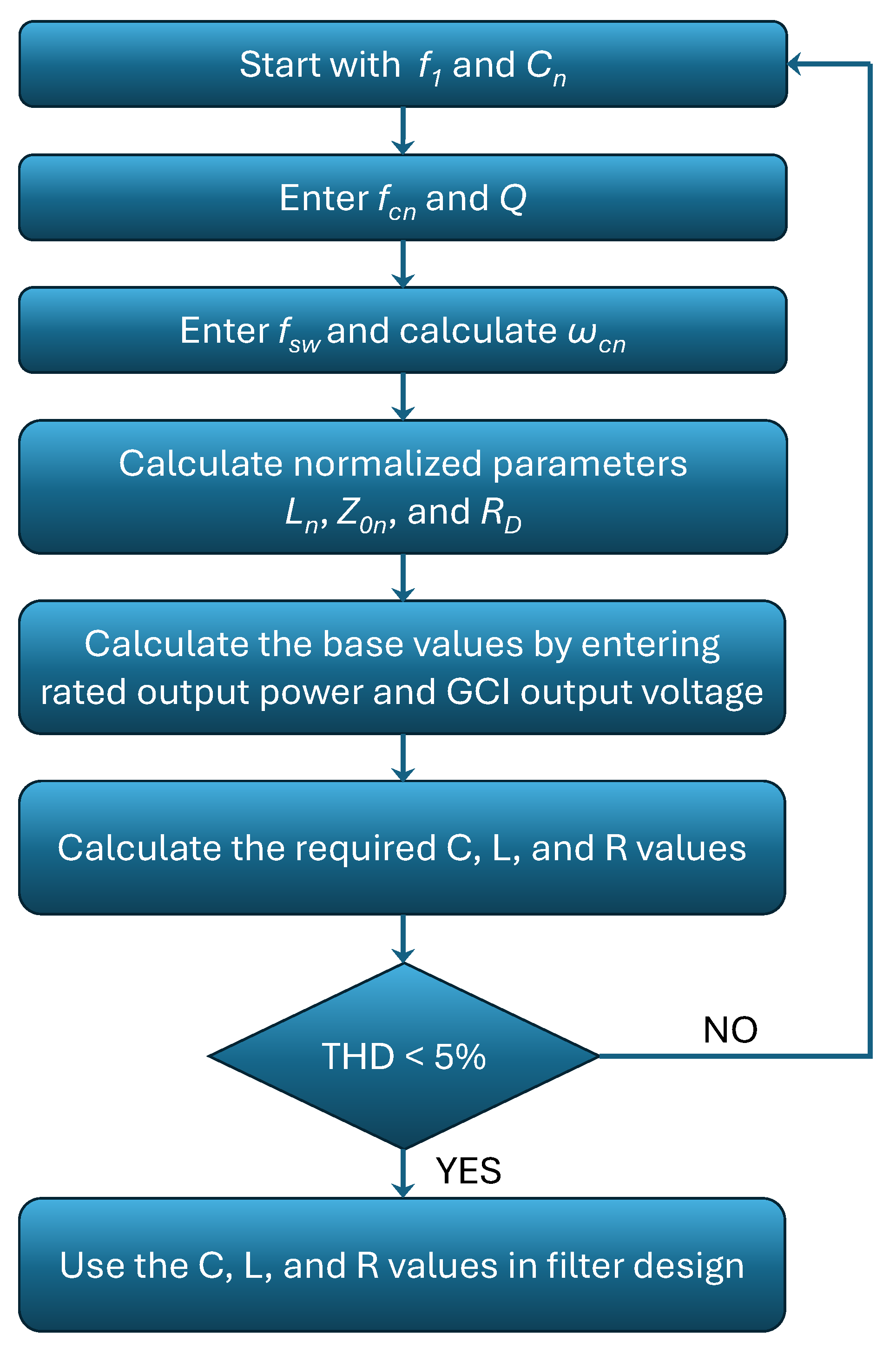
4.1. Filter Design Steps
- Select the switching frequency for the inverter.
- Decide which filter configuration to use.
- Determine the normalized capacitor value to maintain the leading power factor standard ( pu).
- Utilize the contour plot of and THD vs. quality factor and cutoff frequency to establish a target for power loss and THD, ensuring THD and .
- Calculate the value of the inductor to obtain the required cutoff frequency.
- Calculate the damping resistance to obtain the desired quality factor.
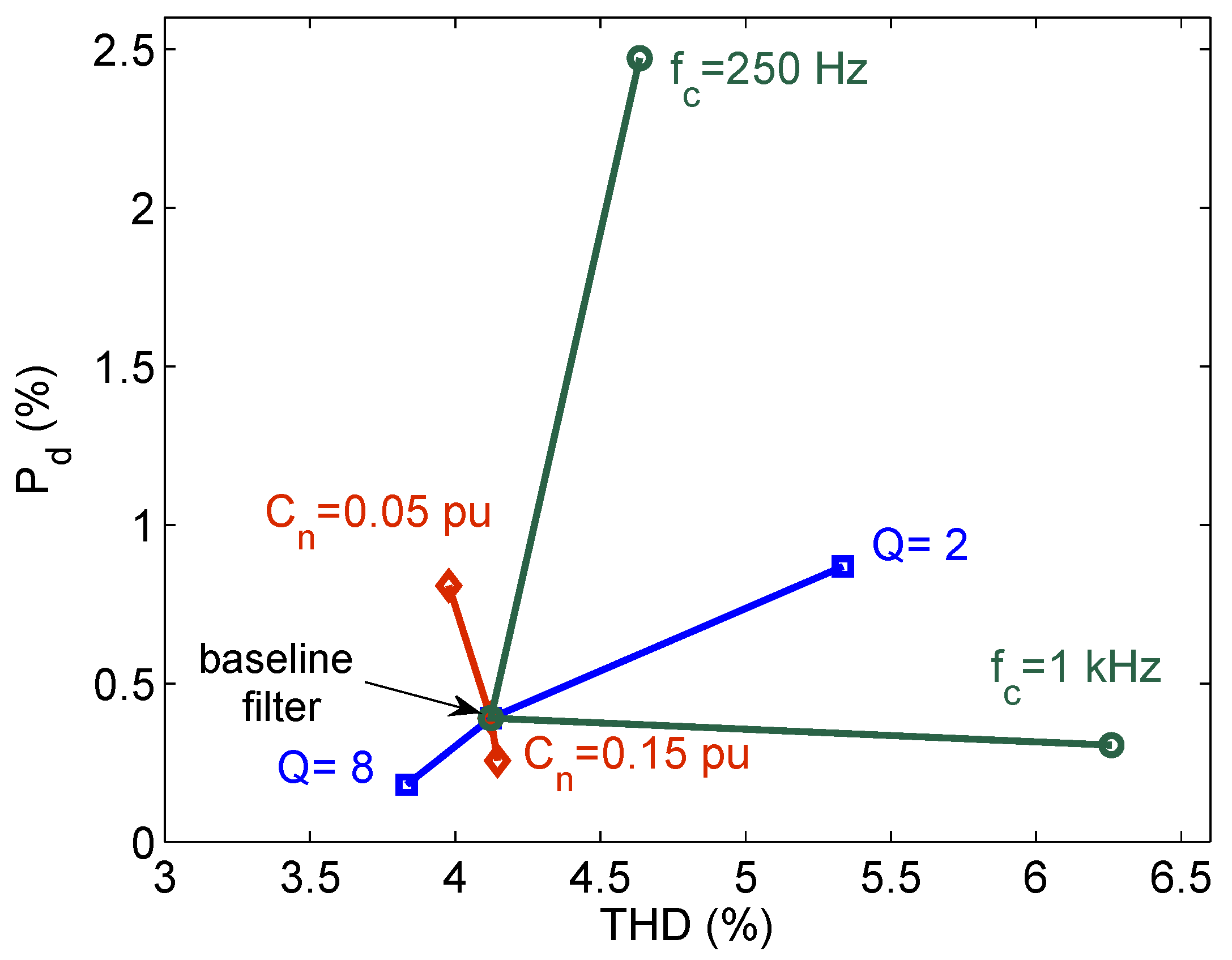
4.2. Effect of Cn Variation
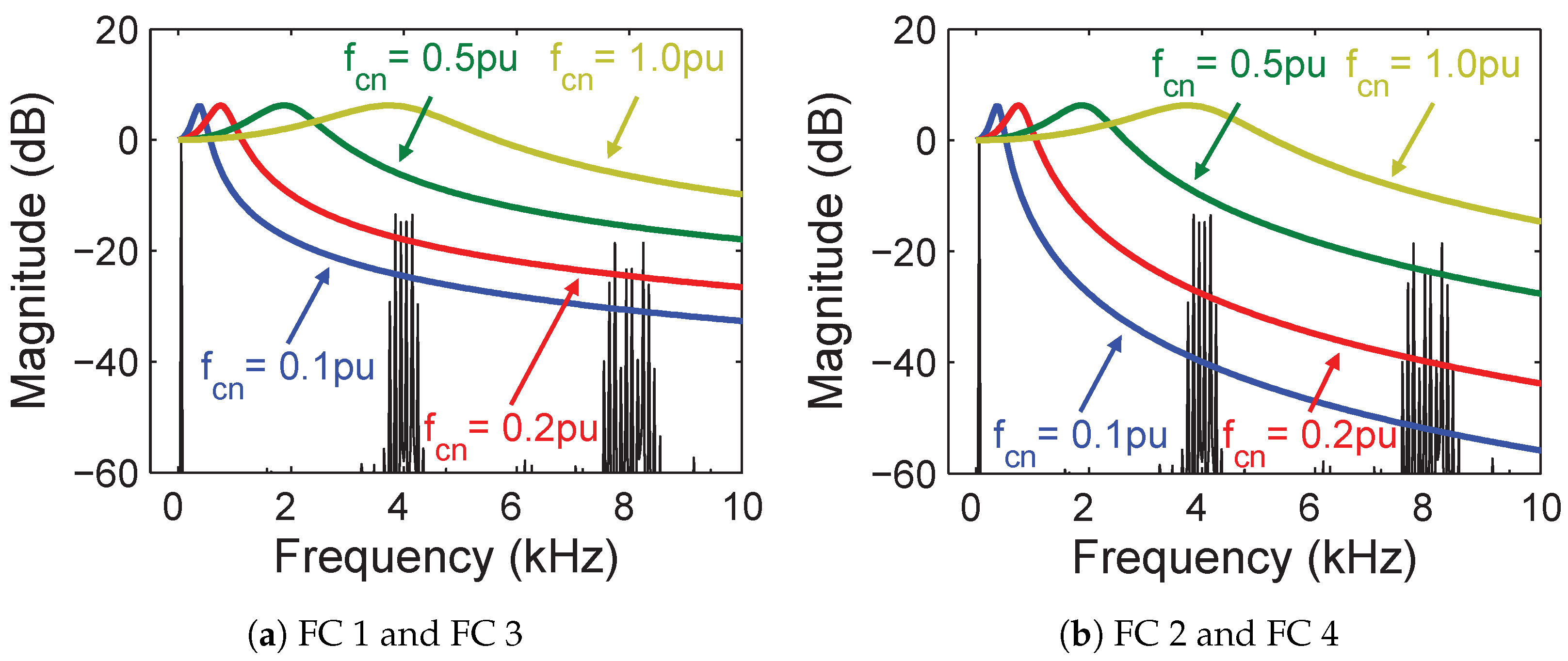
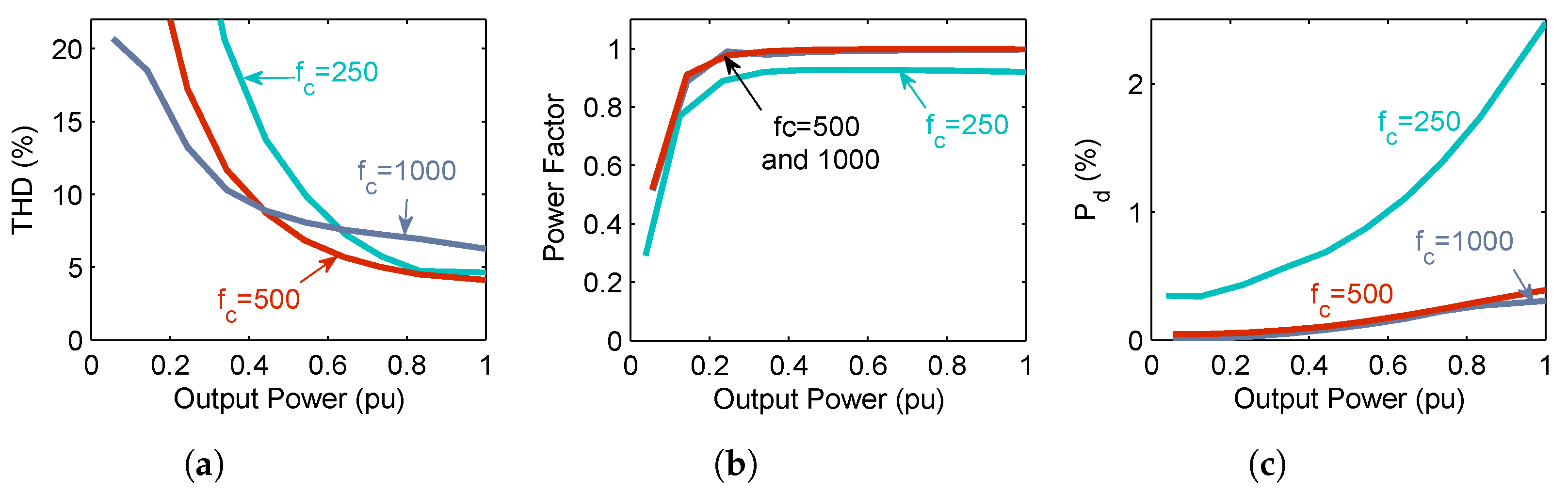
4.3. Effect of fc Variation
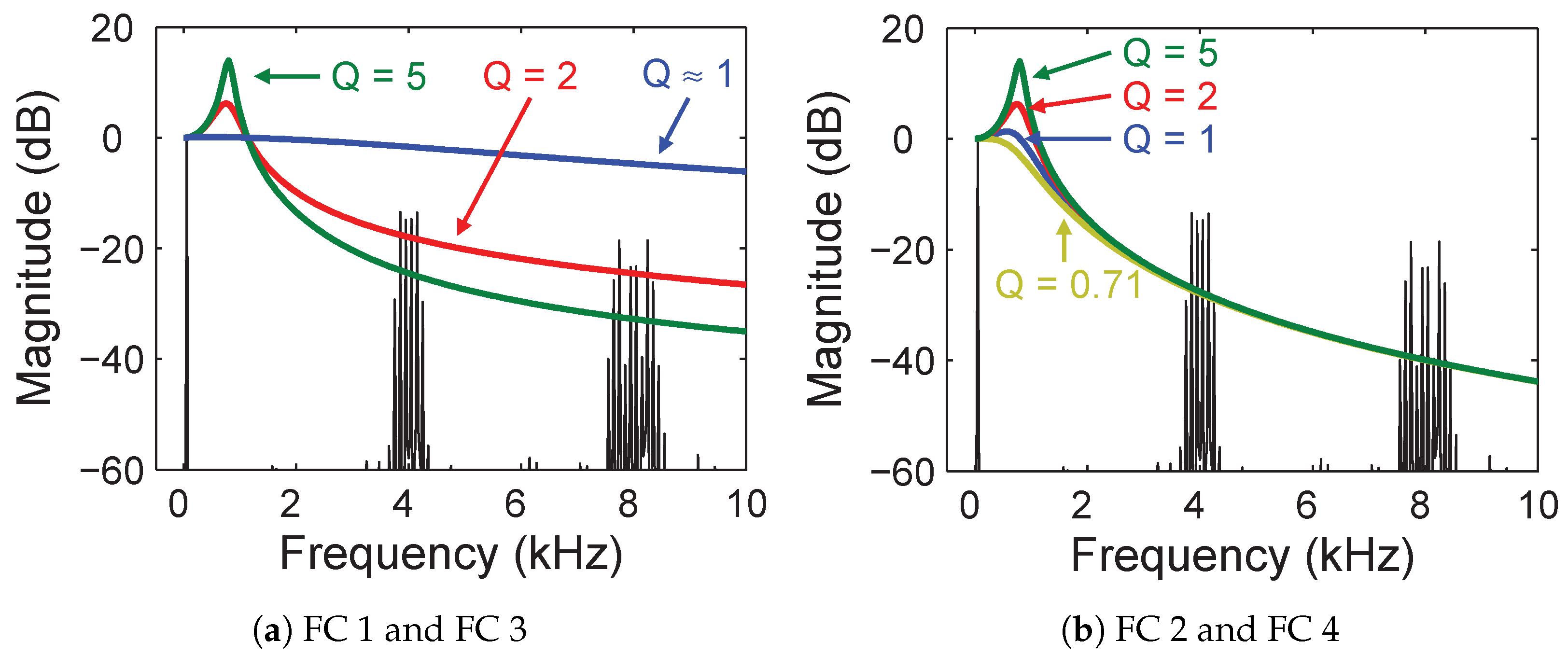
4.4. Effect of Q Variation
4.5. Summary of Effects of Variations
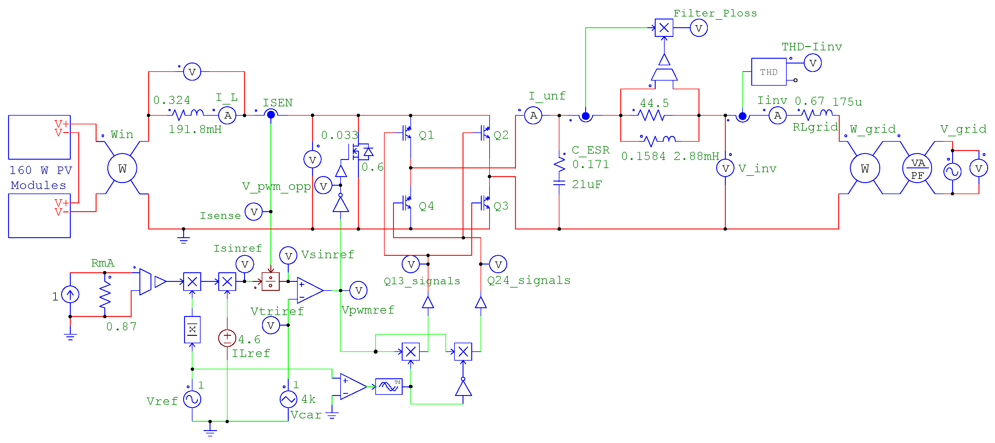
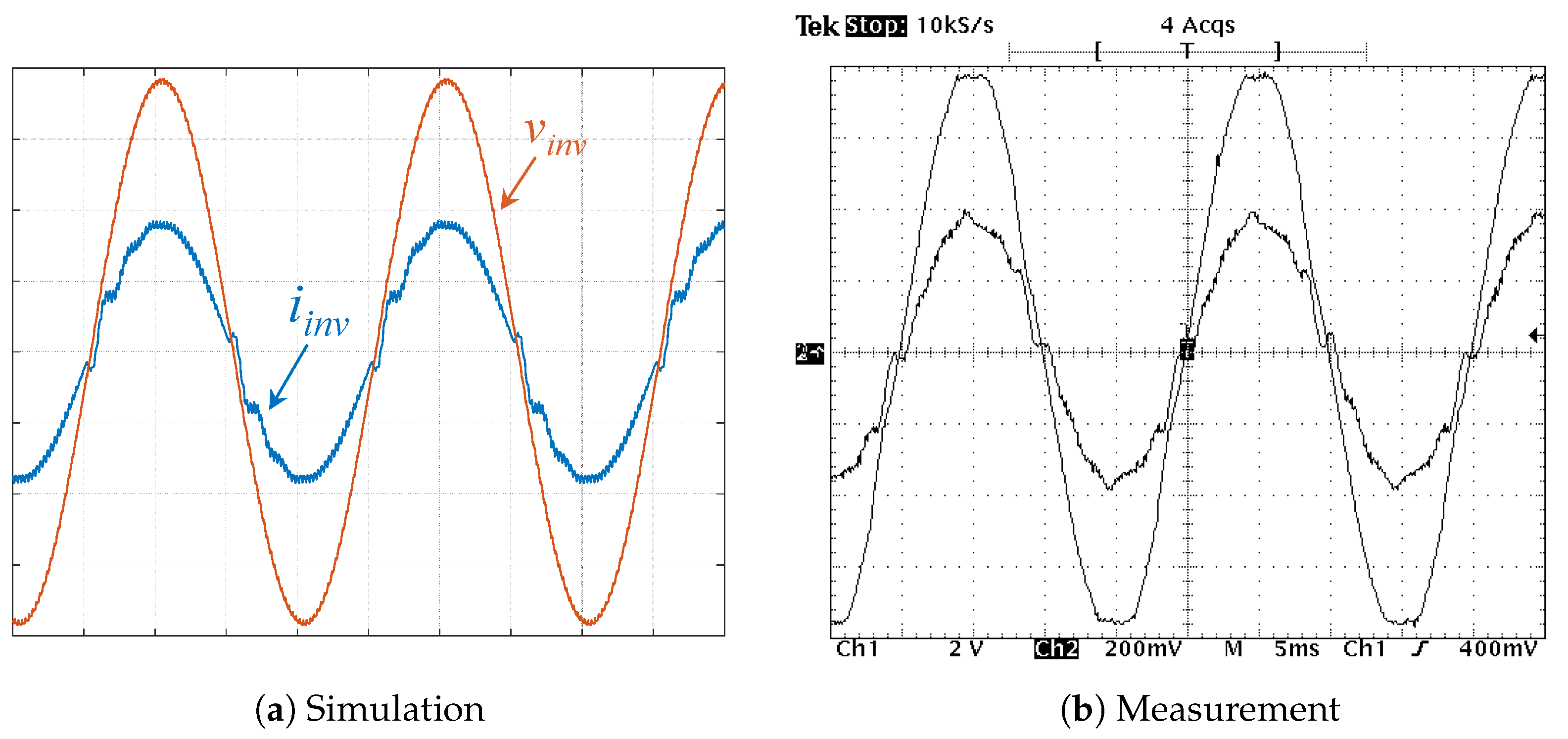
5. Experimental Validation of CL Filter Design
6. Conclusions
Author Contributions
Funding
Institutional Review Board Statement
Informed Consent Statement
Data Availability Statement
Conflicts of Interest
Abbreviations
| CL | Capacitive–inductive low-pass filter |
| CLC | Capacitive–inductive–capacitive low-pass filter |
| CSI | Current-source inverter |
| FC | Filter configuration |
| GCI | Grid-connected inverter |
| L | Inductive low-pass filter |
| LC | Inductive–capacitive low-pass filter |
| LCL | Inductive–capacitive–inductive low-pass filter |
| PF | Power factor |
| PV | Photovoltaic |
| RB-IGBT | Reverse Blocking Insulated Gate Bipolar Transistor |
| PWM | Pulse-width modulation |
| THD | Total harmonic distortion |
| VSI | Voltage-source inverter |
References
- Nave, M. Power Line Filter Design for Switched-Mode Power Supplies, 2nd ed.; Van Nostrand Reinhold: New York, NY, USA, 2010. [Google Scholar]
- Kim, S.-D.; Tran, T.V.; Yoon, S.-J.; Kim, K.-H. Current Controller Design of Grid-Connected Inverter with Incomplete Observation Considering L-/LC-Type Grid Impedance. Energies 2024, 17, 1855. [Google Scholar] [CrossRef]
- Kjaer, S.B.; Pedersen, J.K.; Blaabjerg, F. A review of single-phase grid-connected inverters for photovoltaic modules. IEEE Trans. Ind. Appl. 2005, 41, 1292–1306. [Google Scholar] [CrossRef]
- Cha, H.; Vu, T.-K. Comparative analysis of low-pass output filter for single-phase grid-connected Photovoltaic inverter. In Proceedings of the IEEE Applied Power Electronics Conference and Exposition, Palm Springs, CA, USA, 21–25 February 2010; pp. 1659–1665. [Google Scholar]
- Serpa, L.A.; Ponnaluri, S.; Barbosa, P.M.; Kolar, J.W. A modified direct power control strategy allowing the connection of three-phase inverters to the grid through LCL filters. IEEE Trans. Ind. Appl. 2007, 43, 1388–1400. [Google Scholar] [CrossRef]
- Ahmed, K.H.; Finney, S.J.; Williams, B.W. Passive filter design for three-phase inverter interfacing in distributed generation. Electr. Power Qual. Util. 2007, 13, 49–58. [Google Scholar]
- Adamas-Pérez, H.; Ponce-Silva, M.; Mina-Antonio, J.D.; Claudio-Sánchez, A.; Rodríguez-Benítez, O.; Rodríguez-Benítez, O.M. A New LCL Filter Design Method for Single-Phase Photovoltaic Systems Connected to the Grid via Micro-Inverters. Technologies 2024, 12, 89. [Google Scholar] [CrossRef]
- Channegowda, P.; John, V. Filter optimization for grid interactive voltage source inverters. IEEE Trans. Ind. Electron. 2010, 57, 4106–4114. [Google Scholar] [CrossRef]
- Lindgren, M.; Swenson, J. Control of a voltage-source converter connected to the grid through an lcl filter application to active filtering. In Proceedings of the IEEE Power Electronics Specialists Conference, Fukuoka, Japan, 17–22 May 1998; pp. 229–235. [Google Scholar]
- IEEE Std 1547; Standard for Interconnecting Distributed Resources with Electric Power Systems. IEEE Standards Association: Piscataway, NJ, USA, 2003.
- AS/NZS 4777.2; Grid Connection of Energy Systems via Inverters, Part 2: Inverter Requirements. Standards Australia: Sydney, Australia, 2020.
- Guo, W.; Chen, T.; Huang, A.Q. A Control Bandwidth Optimized Active Damping Scheme for LC and LCL Filter-Based Converters. IEEE Access 2023, 11, 34286–34296. [Google Scholar] [CrossRef]
- Wang, S.; Cui, K.; Hao, P. Grid-Connected Inverter Grid Voltage Feedforward Control Strategy Based on Multi-Objective Constraint in Weak Grid. Energies 2024, 17, 3288. [Google Scholar] [CrossRef]
- Liserre, M.; Blaabjerg, F.; Hansen, S. Design and control of an LCL-filter-based three-phase active rectifier. IEEE Trans. Ind. Appl. 2005, 41, 1281–1291. [Google Scholar] [CrossRef]
- Villanueva, I.; Vázquez, N.; Vaquero, J.; Hernández, C.; López, H.; Osorio, R. L vs. LCL filter for photovoltaic grid-connected inverter: A reliability study. Int. J. Photoenergy 2020, 2020, 7872916. [Google Scholar] [CrossRef]
- Kim, Y.-J.; Kim, H. Optimal design of LCL filter in grid-connected inverters. IET Power Electron. 2019, 12, 1774–1782. [Google Scholar] [CrossRef]
- Xie, L.; Zeng, S.; Liu, J.; Zhang, Z.; Yao, J. Control and Stability Analysis of the LCL-Type Grid-Connected Converter without Phase-Locked Loop under Weak Grid Conditions. Electronics 2022, 11, 3322. [Google Scholar] [CrossRef]
- Khan, D.; Qais, M.; Sami, I.; Hu, P.; Zhu, K.; Abdelaziz, A.Y. Optimal LCL-filter design for a single-phase grid-connected inverter using metaheuristic algorithms. Comput. Electr. Eng. 2023, 110, 108857. [Google Scholar] [CrossRef]
- Wu, T.-F.; Misra, M.; Lin, L.-C.; Hsu, C.-W. An improved resonant frequency based systematic LCL filter design method for grid-connected inverter. IEEE Trans. Ind. Electron. 2017, 64, 6412–6421. [Google Scholar] [CrossRef]
- Sefa, I.; Ozdemir, S.; Komurcugil, H.; Altin, N. An enhanced lyapunov-function based control scheme for three-phase grid-tied VSI with LCL filter. IEEE Trans. Sustain. Energy 2019, 64, 504–513. [Google Scholar] [CrossRef]
- Solatialkaran, D. Optimal Output Filter Design for Grid-Tied Inverters with GaN-Based Switching Devices. Ph.D. Thesis, The University of Queensland, Brisbane, Australia, 2020. [Google Scholar]
- Rodríguez-Benítez, O.M.; Aqui-Tapia, J.A.; Ortega-Velázquez, I.; Espinosa-Pérez, G. Current Source Topologies for Photovoltaic Applications: An Overview. Electronics 2022, 11, 2953. [Google Scholar] [CrossRef]
- Karafil, A. Effect of passive series damping resistor on single phase grid connected inverter with LCL filter. Pamukkale Univ. J. Eng. Sci. 2020, 26, 927–934. [Google Scholar] [CrossRef]
- Beres, R.N.; Wang, X.; Blaabjerg, F.; Liserre, M.; Bak, C.L. Optimal design of high-order passive-damped filters for grid-connected applications. IEEE Trans. Power Electron. 2016, 31, 2083–2098. [Google Scholar] [CrossRef]
- Bolsi, P.C.; Prado, E.O.; Sartori, H.C.; Lenz, J.M.; Pinheiro, J.R. LCL Filter Parameter and Hardware Design Methodology for Minimum Volume Considering Capacitor Lifetimes. Energies 2022, 15, 4420. [Google Scholar] [CrossRef]
- Ali, R.; Heydari-doostabad, H.; Sajedi, S.; O’Donnell, T. Improved design of passive damping for single phase grid-connected LCL filtered inverter considering impedance stability. IET Power Electron. 2024, 17, 511–523. [Google Scholar] [CrossRef]
- Ertasgin, G.; Whaley, D.M.; Soong, W.L.; Ertugrul, N. Low-pass filter design of a current-source 1-ph grid-connected PV inverter. In Proceedings of the IEEE International Scientific Conference on Power and Electrical Engineering of Riga Technical University, Riga, Latvia, 13–14 October 2016; pp. 1–6. [Google Scholar]
- Jayalath, S.; Hanif, M. CL-filter design for grid-connected CSI. In Proceedings of the IEEE Brazilian Power Electronics Conference and 1st Southern Power Electronics Conference, Fortaleza, Brazil, 29 November–2 December 2015; pp. 1–6. [Google Scholar]
- Bautista-López, D.A.; Mantilla-Arias, M.P.; Patarroyo-Gutierrez, L.D. Bidirectional DC-AC converter for photovoltaic solar system in home electrical networks. Dyna 2023, 229, 51–57. [Google Scholar] [CrossRef]
- Shin, Y.; Lee, J.S.; Lee, K.B. Design of a CLC Filter for Flyback-Type Micro-inverters of Grid-Connected Photovoltaic Systems. IETE J. Res. 2017, 63, 504–513. [Google Scholar] [CrossRef]
- Migliazza, G.; Lorenzani, E.; Immovilli, F.; Buticchi, G. Single-Phase Current Source Inverter with Reduced Ground Leakage Current for Photovoltaic Applications. Electronics 2020, 9, 1618. [Google Scholar] [CrossRef]
- de Macedo, G.B.N.; Martins, D.C.; Coelho, R.F. Design and comparative analysis of CL, CLCL and Trap-CL filters for current source inverters. In Proceedings of the IEEE Industry Applications, Curitiba, Brazil, 20–23 November 2016; pp. 1–8. [Google Scholar]
- Zheng, Y.; Deng, H.; Liu, X.; Guan, Y. Sliding Mode Observer-Based Phase-Locking Strategy for Current Source Inverter in Weak Grids. Energies 2024, 17, 4891. [Google Scholar] [CrossRef]
- Khan, D.; Zhu, K.; Hu, P.; Waseem, M.; Ahmed, E.M.; Lin, Z. Active damping of LCL-filtered grid-connected inverter based on parallel feedforward compensation strategy. Ain Shams Eng. J. 2023, 14, 101902. [Google Scholar] [CrossRef]
- Gholami-Khesht, H.; Davari, P.; Wu, C.; Blaabjerg, F. A Systematic Control Design Method with Active Damping Control in Voltage Source Converters. Appl. Sci. 2022, 12, 8893. [Google Scholar] [CrossRef]
- Yang, X.; Zhang, Z.; Xu, M.; Li, S.; Zhang, Y.; Zhu, X.-F.; Ouyang, X.; Alù, A. Digital non-Foster-inspired electronics for broadband impedance matching. Nat. Commun. 2024, 15, 4346. [Google Scholar] [CrossRef] [PubMed]
- Seifi, K.; Moallem, M. An adaptive PR controller for synchronizing grid-connected inverters. IEEE Trans. Ind. Electron. 2019, 66, 2034–2043. [Google Scholar] [CrossRef]
- Whaley, D.M.; Ertasgin, G.; Soong, W.L.; Ertugrul, N.; Darbyshire, J.; Dehbonei, H.; Nayar, C.V. Investigation of a low-cost grid-connected inverter for small-scale wind turbines based on a constant-current source PM generator. In Proceedings of the IEEE Industrial Electronics, Paris, France, 6–10 November 2006; pp. 4297–4302. [Google Scholar]
- Ertasgin, G.; Soong, W.L.; Ertugrul, N. Performance analysis of a low-cost current-source 1-ph grid-connected PV inverter. Turk. J. Elect. Eng. Comp. Sci. 2015, 23, 1985–1991. [Google Scholar] [CrossRef]
- He, Q.; Liu, L.; Qiu, M.; Luo, Q. A Step-by-Step Design for Low-Pass Input Filter of the Single-Stage Converter. Energies 2021, 14, 7901. [Google Scholar] [CrossRef]
- Zhang, J.; Yang, R.; Zhang, C. High-Performance Low-Pass Filter Using Stepped Impedance Resonator and Defected Ground Structure. Electronics 2019, 8, 403. [Google Scholar] [CrossRef]


| Harmonic Order | Limit for Each Harmonic Based on % of Fundamental |
|---|---|
| 2–9 | 4% |
| 10–15 | 2% |
| 16–21 | 1.5% |
| 22–33 | 0.6% |
| Even harmonics | 25% of equivalent odd harmonics |
| Total harmonic distortion (to the 50th harmonic) | 5% |
| Variable | Resonant Frequency, | Quality Factor, | Harmonic Attenuation | Damping Resistor Power Loss, | |
|---|---|---|---|---|---|
| Parameter | |||||
| Inductance, L | ✓ | ✓ | ✓ | ✓ | |
| Capacitance, C | ✓ | ✓ | ✓ | ✓ | |
| Damping resistance, | ✗ | ✓ | ✓ | ✓ | |
| Filter configuration (FC) | ✗ | ✓ | ✓ | ✓ | |
| Power | Apparent (S) | Real (P) | Reactive (Q) | ||
|---|---|---|---|---|---|
| Grid Extremes | |||||
| Power factor = 0.80 lead | 0.20 pu | 0.16 pu | −0.12 pu | 36.9° | |
| Power factor = 0.95 lag | 1.00 pu | 0.95 pu | 0.31 pu | −18.2° | |
| FC | Circuit | Transfer | Quality | Roll-Off Rate |
|---|---|---|---|---|
| Function | Factor | Beyond | ||
| 1 | 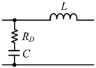 | −20 dB/decade | ||
| 2 |  | −40 dB/decade | ||
| 3 |  | −20 dB/decade | ||
| 4 | 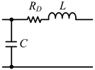 | −40 dB/decade |
| Parameter | Prototype 1 | Prototype 2 |
|---|---|---|
| Rated maximum input power () | 82 W | 164 W |
| Input current for () | 4.5 A | 4.5 A |
| Input voltage () | 17.5 V | 35 V |
| DC link inductance () | 82 mH | 192 mH |
| DC link inductance energy storage (E) | ≈10 mJ/W | ≈12 mJ/W |
| DC link inductor resistance () | 1.3 | 0.33 |
| Filter inductance () | 0.2–0.3 mH | 2.9 mH |
| Filter capacitance () | 100–600 F | 21 F |
| Filter inductor resistance () | 0.3 | 0.16 |
| Filter damping resistance () | 0.3–0.5 | 44.5 |
| PWM switching frequency | 4 kHz | 4 kHz |
| Setup | Filter | Q | Arrangement | THD | ||
|---|---|---|---|---|---|---|
| Prototype 1 | 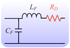 | 2 | 649 Hz | 0.33 pu | Resistive load Resistive + grid Grid | 9.27% 16.0% 21.2% |
| Prototype 2 |  | 4 | 500 Hz | 0.12 pu | Resistive load Resistive + grid Grid | 3.3% 6.1% 7.2% |
Disclaimer/Publisher’s Note: The statements, opinions and data contained in all publications are solely those of the individual author(s) and contributor(s) and not of MDPI and/or the editor(s). MDPI and/or the editor(s) disclaim responsibility for any injury to people or property resulting from any ideas, methods, instructions or products referred to in the content. |
© 2024 by the authors. Licensee MDPI, Basel, Switzerland. This article is an open access article distributed under the terms and conditions of the Creative Commons Attribution (CC BY) license (https://creativecommons.org/licenses/by/4.0/).
Share and Cite
Ertasgin, G.; Whaley, D.M. Analysis and Optimization of Output Low-Pass Filter for Current-Source Single-Phase Grid-Connected PV Inverters. Appl. Sci. 2024, 14, 10131. https://doi.org/10.3390/app142210131
Ertasgin G, Whaley DM. Analysis and Optimization of Output Low-Pass Filter for Current-Source Single-Phase Grid-Connected PV Inverters. Applied Sciences. 2024; 14(22):10131. https://doi.org/10.3390/app142210131
Chicago/Turabian StyleErtasgin, Gurhan, and David M. Whaley. 2024. "Analysis and Optimization of Output Low-Pass Filter for Current-Source Single-Phase Grid-Connected PV Inverters" Applied Sciences 14, no. 22: 10131. https://doi.org/10.3390/app142210131
APA StyleErtasgin, G., & Whaley, D. M. (2024). Analysis and Optimization of Output Low-Pass Filter for Current-Source Single-Phase Grid-Connected PV Inverters. Applied Sciences, 14(22), 10131. https://doi.org/10.3390/app142210131