Article

Large-Area Thickness Measurement of Transparent Films Based on a Multichannel Spectral Interference Sensor

Jihua Laboratory, Foshan 528200, China
*
Author to whom correspondence should be addressed.
Appl. Sci. 2024, 14(7), 2816; https://doi.org/10.3390/app14072816
Submission received: 21 February 2024 / Revised: 23 March 2024 / Accepted: 25 March 2024 / Published: 27 March 2024
(This article belongs to the Section Surface Sciences and Technology)

Abstract

:

Featured Application

Online thickness monitoring of transparent film.

Abstract

Thickness measurement of thin films is essential for quality control in the manufacturing process of the semiconductor and display industries. Real-time monitoring of film thickness during production is an urgent technical problem to be solved. In this study, a method for large-area thickness measurement of transparent films based on a multichannel spectral interference sensor is proposed. The sensor simultaneously acquires multichannel spectral interference signals through a combination of fan-out fiber optic bundles, detection probes, and an imaging spectrometer. The spectral data are calibrated and transformed into the wavenumber dimension, and then the power spectral density estimation method is used to demodulate the data frequency to swiftly derive the film thickness. The thickness measurement capacity of the proposed system is successfully validated on two standard film samples with a relative deviation of less than 0.38% and a relative standard deviation of less than 0.044%. The total spectral acquisition and calculation time for a single multichannel measurement was approximately 7.5 ms. The experimental results on polyimide films show that the measurement efficiency of the system is at least 4 times higher than that of the traditional system, indicating the potential of the multichannel spectral interference sensor for online monitoring in film production.

1. Introduction

Transparent film, as an important industrial component, is widely used in modern optics, semiconductors, displays, and other related scientific and technological fields [1,2,3]. The thickness of thin films produced by physical or chemical deposition methods is directly related to the optical properties, barrier performance, and tensile properties of subsequent applications [4,5,6]. However, multiple production factors such as emission characteristics, preparation environment, relative position placement, and surface shape of the plated parts, might result in uneven thickness distribution, which ultimately affects the product quality [7,8,9]. Online film thickness monitoring is thus particularly important for predicting application effects, modifying process parameters, and improving product quality. Limited by the irregular production environment and cost, there is an urgent need for a fast, accurate, and robust online film thickness measurement system.
Non-contact techniques, such as ultrasonic, ray, terahertz, and optical methods, can be used for online film thickness measurement. Ultrasonic-based technology detects the thickness of a material by accurately measuring the time of ultrasonic wave propagation. Commonly used for oil film thickness monitoring, ultrasonic-based thickness measurement technology features a wide measurement range but suffers from low detection accuracy [10,11,12]. Ray radiation technology obtains the film thickness by detecting the attenuation of the ray intensity after penetrating the object. Despite that the ray radiation methods demonstrate the capacity for high-precision real-time film thickness measurement, the radioactive sources are expensive and highly hazardous [13,14,15]. Terahertz time-domain spectroscopy (THz-TDS) utilizes the time-of-flight (TOF) and resonance frequencies to acquire the thickness of the films. THz-TDS is commonly used for thickness measurement of non-transparent coatings [16,17,18]. The flaws of the two methods render them unsuitable for online thickness measurement in film production.
Among various optics-based methods for thickness measurement, including optical reflection contrast (ORC), spectroscopic ellipsometry (SE), structured illumination microscopy (SIM), chromatic confocal, optical interferometry, and spectral interferometry, ORC is based on the film thickness calculation by capturing the reflectance at certain specific wavelengths with a simple optical configuration. However, for materials with high absorbance, the detectable thickness range is limited to tens of nanometers due to the saturation of the reflected signal with increasing thickness [4,19]. SE is a non-destructive, noncontact, and non-invasive optical technique that is based on the change in the polarization state of light as it is reflected obliquely from a thin film sample. Despite the capacities of spectroscopic ellipsometry for measuring the thickness, reflectance, and refractive index of thin films from sub-micron to nanometer scale [20,21], the application of the technique is limited by additional measurement time, a small thickness measuring range, and a complicated structure. SIM can obtain the surface profiles and film thickness by detecting the peaks of the modulation depth response curves [22,23]. It can detect micrometer-thick films but cannot be used for industrial inspection due to its slow detection speed. Chromatic confocal microscopy converts the axial position of the film surface into spectral information through a confocal pinhole in front of the spectrometer; hence, the measurable thickness range is restricted by spectral bandwidth and resolution [24]. Based on the principle of optical interferometry, laser interferometry [25], white light interferometry [26], and differential interferometry [27] have been developed to achieve nanometer thickness measurement accuracy in the millimeter measurement range. The industrial applications of these methods are also constrained by the high cost and strict requirements of environmental conditions.
Analyzing the modulation period of the spectral interference fringes, spectral interferometry calculates thickness, which has the advantage of being simple, nondestructive, and cost-effective [28,29,30]. Although its film-measurable thickness range is limited by the spectral bandwidth and resolution in principle, commercial spectrometers can be used to measure films in the thickness range of submicron to submillimeter. The thickness measurement accuracy of transparent films is influenced by system parameters and calculation methods. The major film thickness calculation methods developed using the interference spectrum include the extremum method [31], envelope method [32], full-spectrum fitting method [33], and frequency analysis [34]. The extremum method searches for adjacent spectral peaks corresponding to wavelengths and is easily affected by the accuracy of the curve fitting. The envelope method and the full-spectrum fitting method depend greatly on the reflectivity model, rendering them susceptible to non-ideal signals with noise and distortion of baselines in real-life measurements. The frequency analysis method calculates the film thickness by extracting the phase information from the high-frequency section of the spectral signal, thereby filtering out the influence of the light source and ambient light. This method relies less on the reflectivity model and can obtain thickness with sub-micro accuracy through a relatively cumbersome calculation process. Benefited by a simple configuration, spectral interferometry poses the potential for industrial thickness measurement of transparent films. However, limited by accuracy, speed, and a single-point measurement process, the existing technique is still incapable of large-area thickness measurement of transparent films during manufacturing.
In this study, a multichannel spectral interference sensor was designed for measuring large-area and multi-layer thicknesses of transparent films. Linear 1-to-4 fan-out fiber optic bundles were used to connect multiple probes to the imaging spectrometer. The probes detected the spectral interference signal of transparent films at a vertical angle and could be arranged according to the actual location. The film thickness was calculated by fitting the peak of the power spectral density estimate for the spectral interference signal in the wavenumber domain. To verify the effectiveness and accuracy of the proposed method, two standard film samples of different thicknesses and varieties were employed for testing. The extremum method and the Fourier frequency transform method were compared with the proposed method. In addition, experiments on polyimide films demonstrated the real-time multilayer measurement and thickness imaging capabilities of the proposed method, which supported its potential application in industrial inspection.

2. Methods

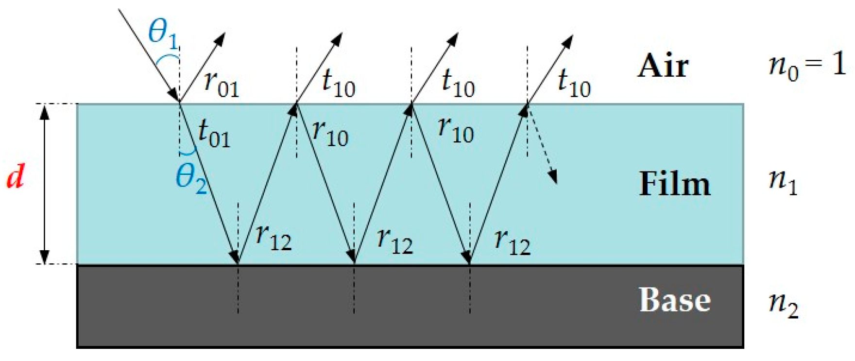
2.1. Basic Principle

Figure 1 shows a schematic of multiple interferences of the monolayer as illustrated elsewhere [35,36]. The incident light with an angle of θ1 through the air media with a refractive index of n0 was reflected at the surface with a reflection coefficient of r01 and transmitted to the film media of n1 with a transmission coefficient of t01. The incident light with an angle of θ2 through the film media with a thickness of d was reflected at the surface of n1n2 with a reflection coefficient of r12. The reflected light reached the surface of the air-film, was reflected at the surface with r10, and was transmitted to the air media with t10. The iteration of the procedure would produce interference from the transparent film. The spectral intensity changes periodically in the wavelength dimension. The film thickness can be resolved from the spectral interference signal.
Without considering the absorption of light by the film, the amplitude of the electric field can be summed as
E = E 1 + E 2 + E 3 + E 4 + = E 0 ( r 01 + t 01 r 12 t 10 e i Δ + t 01 r 12 2 r 10 t 10 e 2 i Δ + t 01 r 12 3 r 10 2 t 10 e 3 i Δ + ) = E 0 ( r 01 + t 01 r 12 t 10 e i Δ × 1 ( r 12 r 10 e i Δ ) n 1 r 12 r 10 e i Δ ) E 0 r 01 + r 12 e i Δ 1 r 12 r 10 e i Δ ,
where E0 is the original electric field amplitude, and Ei is the electric field amplitude returned from the surface of the air-film. Δ is the phase difference passing through V-shaped optical paths, which can be expressed as
Δ = 4 π n 1 d cos θ 1 / λ .
Then, the constructive interference condition can be expressed as Δ = 2 k π (k is an integer). When the angle of incident light is close to 0°, the adjacent maxima of spectra are given by the wavelengths λ1 < λ2,
4 π n 1 d ( 1 λ 1 1 λ 2 ) = 2 π
According to Equation (3), the frequency and period of spectral interference signal can be expressed as T = 1 f = 1 λ 1 1 λ 2 , and then the thickness of d can be calculated using
d = 1 2 n 1 T = f 2 n 1

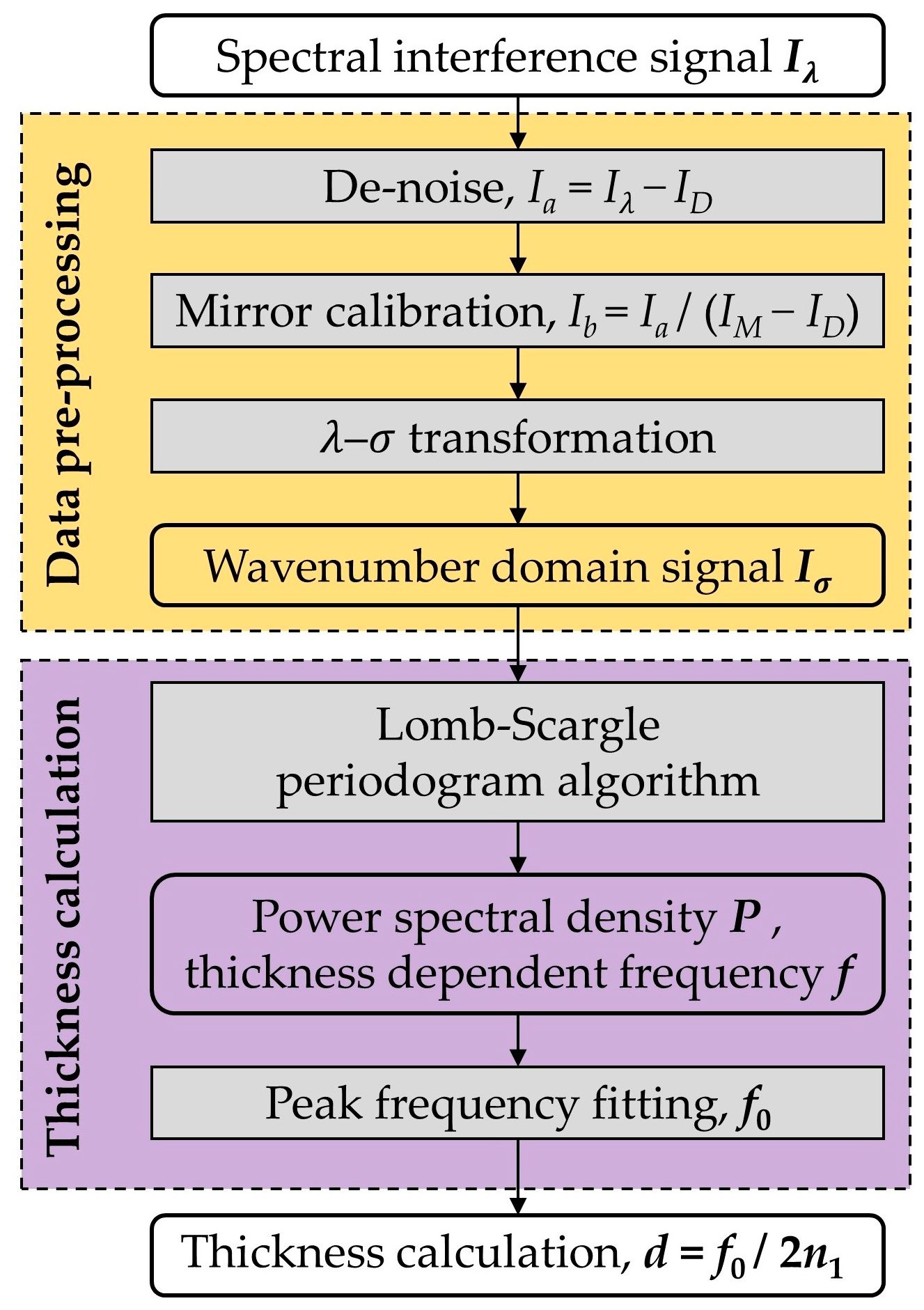
2.2. Calculation Method

Figure 2 shows the flow chart of the calculation method in this paper. Firstly, the dark noise was subtracted from the original interference signal, and a standard mirror was used to eliminate the influences of the light source and optical system. Second, the calibrated signal was transformed into the wavenumber domain. Third, the Lomb–Scargle periodogram power spectral density estimation algorithm was used to process the unevenly sampling data in the wavenumber domain, and calculate the power spectral density P and frequency f. Finally, the peak value of the power spectral density function was extracted by the quadratic linear fitting method to calculate the film thickness.
Due to the wavelength drift of the spectrometer and the reciprocal transformation from the wavelength to the wavenumber domain, the non-uniform sampled characteristic of σ made Iσ unable to be directly analyzed by the conventional spectral analysis method. The Lomb–Scargle periodogram (LSP) [31,37] is a widely used algorithm for detecting and characterizing periodicity in unevenly sampled data. It is particularly suitable for extracting the period or frequency of unevenly sampled interference signals in the wavenumber domain. The LSP function applied in the wavenumber-phase factor domain (σz) is defined as
P L S ( z ) = 1 2 { [ n I n cos ( 2 π z ( σ n τ ) ) ] 2 n cos 2 ( 2 π z ( σ n τ ) ) + [ n I n sin ( 2 π z ( σ n τ ) ) ] 2 n sin 2 ( 2 π z ( σ n τ ) ) }
where τ is specified for each z to ensure time-shift invariance,
τ = 1 4 π z tan 1 ( n sin ( 4 π z σ n ) n cos ( 4 π z σ n ) )
The power spectral density estimate of the spectral interference signal is discrete and sparse. Limited by the sampling rate of the spectrometer, the minimum frequency interval converts to an actual thickness of about 30–60 nm. Therefore, there is an inherent error in extracting film thickness directly by finding the frequency corresponding to the maximum power spectral density. To further improve the calculation accuracy of film thickness, data with an amplitude greater than 50% of the peak value of power spectral density were used to calculate the final film thickness by quadratic linear fitting. Therefore, using the built-in complete method to calculate the film thickness can greatly eliminate the false-frequency interference caused by environmental noise and improve the accuracy of the system.

2.3. Hardware Configuration

Figure 3 shows the optical layout and experimental system to simultaneously measure the thicknesses of multiple points. Considering the measurement principle of spectral interference, a Tungsten/Halogen lamp (KEWLAB, HLS-1, Melbourne, VIC, Australia), which covers a wide wavelength range from 360 nm to 2500 nm with a fiber output power of 5 mW, was used as the light source. An imaging spectrometer (Princeton Instruments, IsoPlane-160, Teledyne Princeton Instruments, Trenton, NJ, USA) with camera pixels of 1024 × 1024 was used as a detector. The spectral resolution of the spectrometer is 1.2 nm in the wavelength range from 440 nm to 850 nm. Therefore, according to Equation (3), the film thickness measurement range that the proposed system can achieve was calculated at about 250 nm to 90 μm. A doublet lens with a focal length of 60 mm was used to construct the detection probe, and the spot size was approximately 1 mm. Linear 1-to-4 fan-out fiber bundles (Xinrui, SUH600, Shenzhen, China) with a core diameter of 600 μm were used to connect multiple probes to the imaging spectrometer. In particular, the light collected by the fiber bundles imaged on the spectrometer slit could be distinguished by the imaging spectrometer. In the experimental configuration, the slit length was 15 mm, and the slit width was set to 10 μm to ensure high spectral resolution. While the imaging diameter of the single fiber core on the spectrometer slit was less than 1 mm, the imaging spectrometer could be used to measure the film thickness in up to 15 channels. The film thickness calculation program was run on the MATLAB (R2022b) platform on a personal computer with an Intel® CoreTM i5-12400F 2.50 GHz processor (Intel Corporation, Santa Clara, CA, USA) and 16.0 GB of memory.

3. Experiments and Discussion

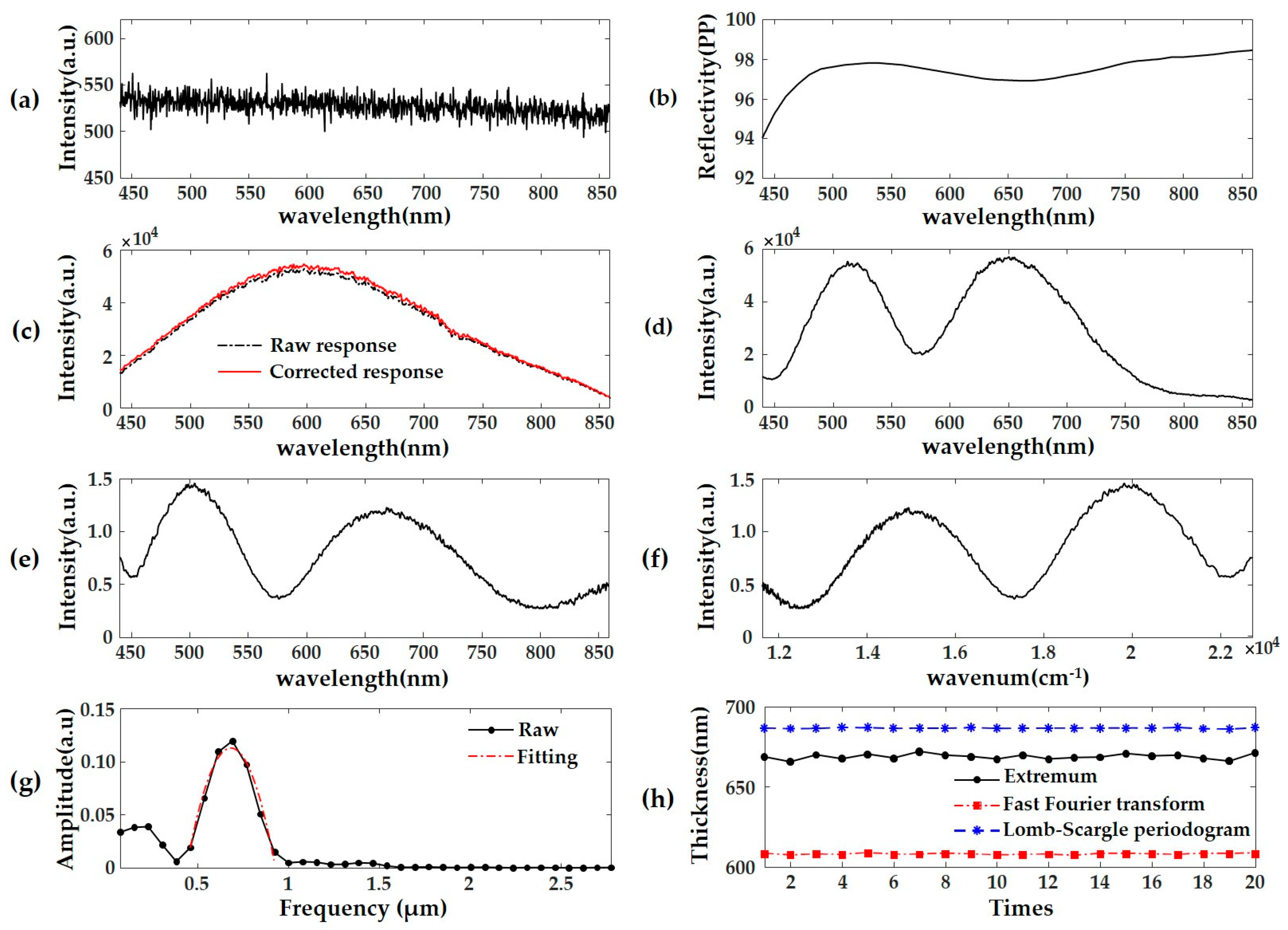
3.1. Standard Film Samples Measurement

Figure 4 shows two standard film samples of different thicknesses and varieties used in this study. The wavelength and linearity of the system were calibrated using a mercury/argon lamp, eliminating the effect of high-order dispersion of the probe. The standard film samples were then measured 20 times at the test point to verify the effectiveness and accuracy of the proposed method.
Figure 5 shows the measurement results of the SiO2 standard film sample. The certified thickness of the SiO2 standard film sample is 689.13 ± 3 nm, and the refractive index is 1.462. The spectral curve was calibrated to an interference curve with a fixed period in the wavenumber domain, as shown in Figure 5f. Figure 5g shows the power spectral density estimate of the spectral interference signal. The film thickness can be extracted by quadratic linear fitting of the peak value corresponding to the frequency. The extremum method, the Fourier frequency transform method, and the proposed method were respectively used to calculate the film thickness, as shown in Figure 5h. Due to the dark noise of the system, several measurement results of the SiO2 standard film sample were different. Limited by the sampling rate of the spectrometer, the minimum frequency interval conversion leads to relatively large deviations in the results of the Fourier frequency transform method. However, the proposed method improves the calculation accuracy of film thickness by quadratic linear fitting of 50% of the peak value of the power spectral density.
The detailed calculation results of the SiO2 standard film sample by the extremum method, the Fourier frequency transform method, and the proposed method are shown in Table 1. The measurement results indicated the mean thickness deviations of these three methods were −20.48 nm, −81.22 nm, and −2.61 nm, respectively. The measurement standard deviations of these three methods were 1.65 nm, 0.26 nm, and 0.27 nm, respectively. Compared with the extremum method and the Fourier frequency transform method, the proposed method was distinguished by a smaller deviation for film thickness. The computing time of the proposed method for a single spectrum was about 1.17 ms, which was longer than that of the other two methods. However, the total measurement and computing time of the proposed method was approximately 3 ms, which can meet the needs of online inspection in industrial production.
The detailed measurement results for the two standard film samples are detailed in Table 2. The certified thickness of the parylene standard film sample is 7166 nm, and the refractive index is 1.661. The maximum deviations of the multichannel measurement results of the two films were −2.61 nm and −15.1 nm, while the maximum standard deviations were 0.30 nm and 1.1 nm, respectively. The results demonstrate that the relative deviation of the system is less than 0.38%, and the relative standard deviation is less than 0.044%. Therefore, the proposed method can meet the requirement of thickness measurement accuracy in film industrial production.

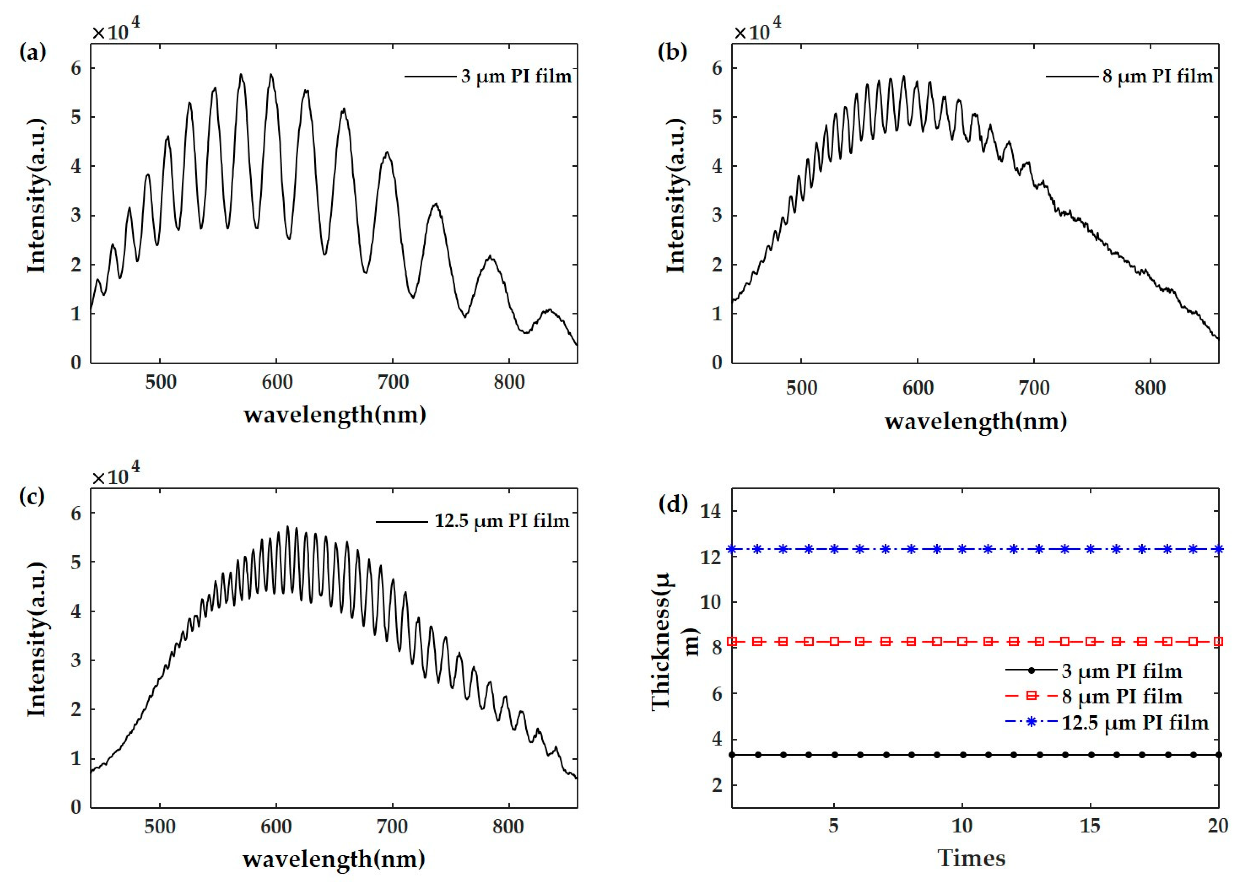
3.2. Thickness Measurement of Polyimide Films

Polyimide films with different thicknesses were used to verify the feasibility of the system for industrial production measurement. Widely used in electrical and electronic fields, polyimide is a polymer material with a low dielectric constant, good heat resistance, and mechanical properties [38,39,40]. Polyimide film products are made from the gel film salivated by the polyamide acid resin solution. Subsequent preparation processes include directional stretching, imidization, and some post-treatment processes. Online thickness monitoring of polyimide films is related to the quality of subsequent products.
PI films can be divided into electrical-grade and electronic-grade films. We measured three electronic-grade polyimide films with various thicknesses, as depicted in Figure 6. The integration time of the spectrometer was set to 3 ms, and other parameters remained unchanged. The nominal thicknesses of these three films are 3 μm, 8 μm, and 12.5 μm, respectively. However, the average thicknesses of these films measured 20 times at the sampling point were 3.3144 μm, 8.2791 μm, and 12.3290 μm, while the standard deviations were 1.74 nm, 7.89 nm, and 24.17 nm, respectively.

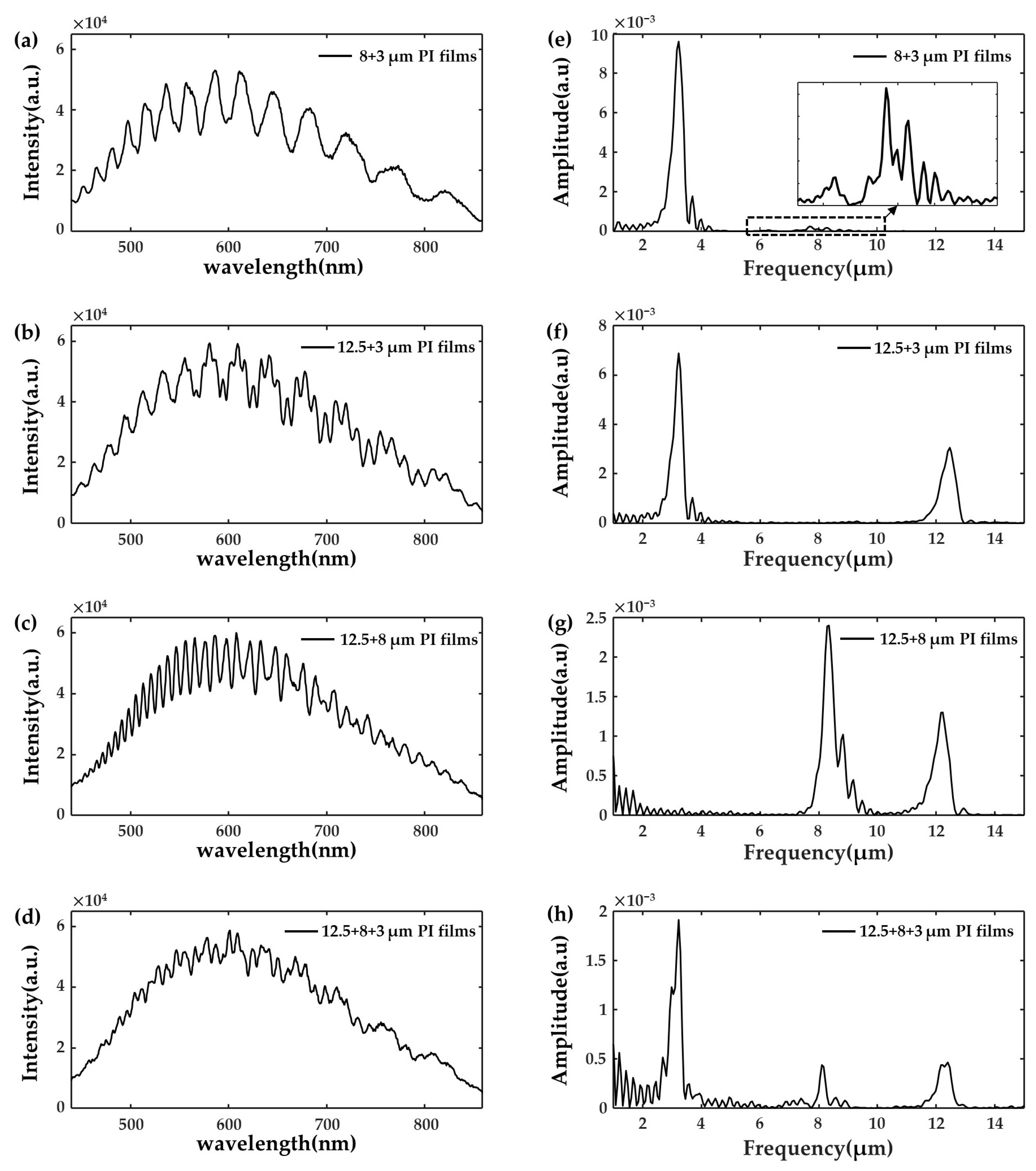
3.3. Multilayer Films Measurement

The proposed system can be further applied to the thickness measurement of multilayer films. The three polyimide films mentioned above were combined to produce four multilayer films. To ensure the signal-to-noise ratio, the integration time of the spectrometer was set to 5 ms, and other parameters remained unchanged. The spectral interference signals of multilayer polyimide films are shown in Figure 7a–d. The spectral period change ceases to follow an intuitive trend with the increase in the number of film layers. Traditional techniques, such as the extremum method, are no longer feasible for the thickness calculation of different film layers. The power spectral density derived by the proposed method is shown in Figure 7e–h. The thickness of the multilayer film can be calculated by fitting the frequencies corresponding to the peaks of the power spectral density curve. However, the amplitude of the power spectral density decreases obviously with the increase in the number of film layers, indicating a limit on the measurable number of film layers. In addition, as shown in Figure 7e, when the signal-to-noise ratio of the spectral interference signal in a certain layer of the multilayer film is low, the power spectral density curve will be disordered and challenging to fit. The uncertainty of the artificial preparation of multilayer films may lead to the occurrence of this phenomenon.
The measurement of the above multilayer films was replicated 10 times. The results detailed in Table 3 demonstrated that the relative standard deviation of the measured multilayer film thickness was less than 0.16%. In addition, with the increase in the number of film layers, the measurement accuracy of the film thickness decreased. The large thickness difference of the same type of film in different combinations indicated poor uniformity of the artificially prepared multilayer film.

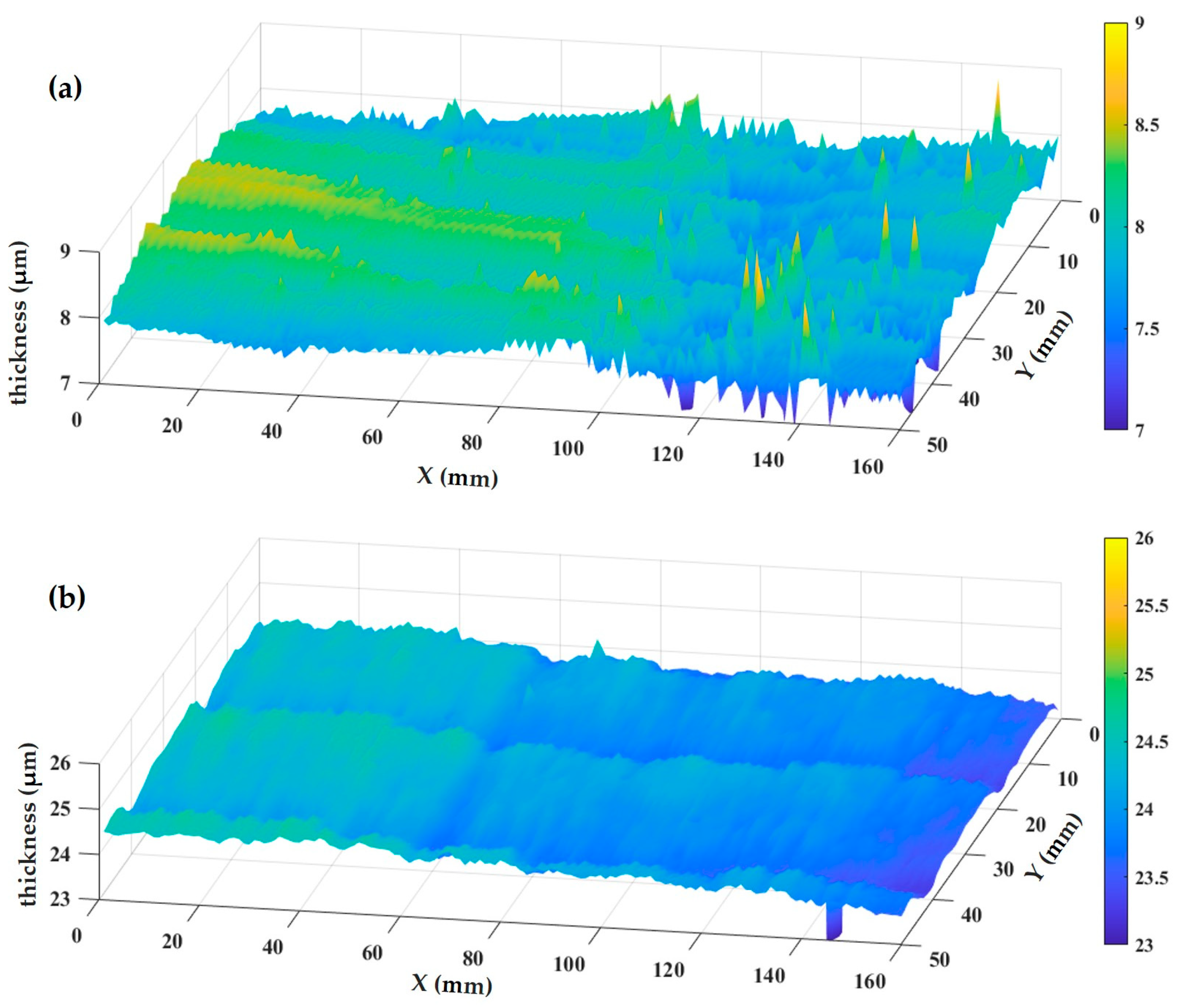
3.4. Large-Area Thickness Measurement

To verify the large-area thickness measurement capability of the proposed method, thickness imaging of two polyimide films of different thicknesses was performed using an XY stage (Thorlabs, MLS203-1, Newton, NJ, USA) with a scanning range of 110 mm × 75 mm. The scanning area of each channel was 50 × 50 mm2, while the XY scanning steps were 1.25 mm and 1 mm, respectively. The measurement speed of the proposed system was 4 times that of a traditional single-point thickness measurement system. The total measurement time was limited to 250 s by the spectrometer frame rate of 8 fps. The scanning speed can be greatly improved by using a spectrometer with a high frame rate camera as the single spectral acquisition, and the following calculation took only 2 ms and 5.5 ms, respectively.
The thickness distribution of the two polyimide films is shown in Figure 8. The mean thicknesses of the two films were 7.919 μm and 24.044 μm, respectively. And the standard deviations were 0.2581 μm and 0.514 μm, respectively. Therefore, the thickness uniformity of the two films was 3.26% and 2.14%, respectively. The sinusoidal fluctuations in the thickness of the film indicated room for improvement in the coating process. Additionally, the observed noise points in the thickness image are related to wrinkles and dust on the film, and thus, the functionality of the proposed method is also affected by the cleanness of the working environment. It is necessary to keep the film flat and the environment clean during online measurement.

4. Conclusions

In this study, a multichannel spectral interference sensor for large-area thickness measurement of transparent films was proposed. In the optical configuration, linear 1-to-4 fan-out fiber bundles were used to connect multiple probes to the imaging spectrometer. Multichannel signals can be detected synchronously, and the integration time is related to the reflectivity of the sample, which is about 2–5 ms. The film thickness measurement range that the proposed system can achieve was calculated at about 250 nm to 90 μm. Furthermore, a complete method combining the power spectral density estimation algorithm and the quadratic linear fitting algorithm was used to calculate film thickness. Compared with the extremum method and the Fourier frequency transform method, the proposed method was distinguished by a smaller deviation for film thickness. The total measurement and computing time of a single-point film thickness was about 3 ms.
To verify the thickness measurement performance of the proposed method, two standard film samples of different thicknesses and varieties were measured 20 times. The results demonstrate that the relative deviation of the system is less than 0.38%, and the relative standard deviation is less than 0.044%. In addition, good performance has been achieved in the thickness measurement experiment of electronic-grade polyimide films. Three different thicknesses of multilayer films were accurately distinguished by just one experiment. Furthermore, the large-area thickness measurement speed of the proposed system was four times that of a traditional single-point thickness measurement system. The large-area thickness measurement experiments revealed the periodic thickness variation of the film, which may be related to the production parameters. In addition, the noise points observed in the thickness images are related to wrinkles and dust on the film. Therefore, it is necessary to keep the film flat and the environment clean during online measurement.
Despite that the scanning speed of film thickness imaging was limited to 6 Hz by the frame rate of the spectrometer and the step time of the scanning stage, the total time for single multichannel spectral acquisition and thickness calculation was successfully reduced to 7.5 ms. The measurement speed can be increased by selecting a spectrometer with a high frame rate camera in future work. We will continue to optimize the algorithm model and the probe design to further improve the accuracy of the measurement system.

Author Contributions

Conceptualization, W.H. and H.B.; methodology, W.H.; validation, Z.T., C.W. and Y.S.; formal analysis, W.H.; investigation, Z.D.; resources, H.B.; data curation, W.H.; writing—original draft preparation, W.H.; writing—review and editing, C.W.; visualization, W.H.; supervision, H.B.; project administration, W.H.; funding acquisition, W.H. and H.B. All authors have read and agreed to the published version of the manuscript.

Funding

This research was funded by the Youth Innovation Foundation of Jihua Laboratory (X220171XP220), the Key Project Foundation of Jihua Laboratory (X210221TP210), and the National Natural Science Foundation of China (52173282).

Data Availability Statement

The raw data supporting the conclusions of this article will be made available by the authors on request.

Conflicts of Interest

The authors declare no conflicts of interest.

References

  1. ElKabbash, M.; Letsou, T.; Jalil, S.A.; Hoffman, N.; Zhang, J.H.; Rutledge, J.; Lininger, A.R.; Fann, C.H.; Hinczewski, M.; Strangi, G.; et al. Fano-resonant ultrathin film optical coatings. Nat. Nanotechnol. 2021, 16, 440–446. [Google Scholar] [CrossRef] [PubMed]
  2. Shi, J.L.; Zhang, J.Y.; Yang, L.; Qu, M.; Qi, D.C.; Zhang, K.H.L. Wide Bandgap Oxide Semiconductors: From Materials Physics to Optoelectronic Devices. Adv. Mater. 2021, 33, 2006230. [Google Scholar] [CrossRef] [PubMed]
  3. Mondal, S.; Yoshida, T.; Maji, S.; Ariga, K.; Higuchi, M. Transparent Supercapacitor Display with Redox-Active Metallo-Supramolecular Polymer Films. ACS Appl. Mater. Interfaces 2020, 12, 16342–16349. [Google Scholar] [CrossRef] [PubMed]
  4. Jin, Y.; Yu, K. A review of optics-based methods for thickness and surface characterization of two-dimensional materials. J. Phys. D-Appl. Phys. 2021, 54, 393001. [Google Scholar] [CrossRef]
  5. Oh, S.J.; Kwon, J.H.; Lee, S.; Choi, K.C.; Kim, T.S. Unveiling the Annealing-Dependent Mechanical Properties of Freestanding Indium Tin Oxide Thin Films. ACS Appl. Mater. Interfaces 2021, 13, 16650–16659. [Google Scholar] [CrossRef] [PubMed]
  6. Chauhan, R.N.; Tiwari, N. Preparation of optically transparent and conducting radio-frequency sputtered indium tin oxide ultrathin films. Thin Solid Film. 2021, 717, 138471. [Google Scholar] [CrossRef]
  7. Butt, M.A. Thin-Film Coating Methods: A Successful Marriage of High-Quality and Cost-Effectiveness—A Brief Exploration. Coatings 2022, 12, 1115. [Google Scholar] [CrossRef]
  8. Benrezgua, E.; Deghfel, B.; Zoukel, A.; Basirun, W.J.; Amari, R.; Boukhari, A.; Yaakob, M.K.; Kheawhom, S.; Mohamad, A.A. Synthesis and properties of copper doped zinc oxide thin films by sol-gel, spin coating and dipping: A characterization review. J. Mol. Struct. 2022, 1267, 133639. [Google Scholar] [CrossRef]
  9. Akhtar, A.; Ruan, H.H. Review on thin film coatings for precision glass molding. Surf. Interfaces 2022, 30, 101903. [Google Scholar] [CrossRef]
  10. Dou, P.; Jia, Y.; Zheng, P.; Wu, T.; Yu, M.; Reddyhoff, T.; Peng, Z. Review of ultrasonic-based technology for oil film thickness measurement in lubrication. Tribol. Int. 2022, 165, 107290. [Google Scholar] [CrossRef]
  11. Dou, P.; Wu, T.; Peng, Z. A time-domain ultrasonic approach for oil film thickness measurement with improved resolution and range. Meas. Sci. Technol. 2020, 31, 075006. [Google Scholar] [CrossRef]
  12. Wei, S.J.; Wang, J.R.; Cui, J.; Song, S.S.; Li, H.C.; Fu, J.F. Online monitoring of oil film thickness of journal bearing in aviation fuel gear pump. Measurement 2022, 204, 112050. [Google Scholar] [CrossRef]
  13. Chen, Z.Q.; Chen, J.J.; Shu, S.B.; Yu, Z.Q.; Zhang, Y.Z.; Tao, X.J.; Lang, X.L. Oil Scale Profile Detection in Oil Pipeline Based on Improved Gamma-Ray Scanning Transmission Method. Nucl. Sci. Eng. 2022, 196, 1255–1265. [Google Scholar] [CrossRef]
  14. Kim, K.J. Review on the thickness measurement of ultrathin oxide films by mutual calibration method. Surf. Interface Anal. 2022, 54, 405–416. [Google Scholar] [CrossRef]
  15. Giurlani, W.; Berretti, E.; Innocenti, M.; Lavacchi, A. Measuring the Thickness of Metal Coatings: A Review of the Methods. Coatings 2020, 10, 1211. [Google Scholar] [CrossRef]
  16. Im, K.H.; Kim, S.K.; Cho, Y.T.; Woo, Y.D.; Chiou, C.P. THz-TDS Techniques of Thickness Measurements in Thin Shim Stock Films and Composite Materials. Appl. Sci. 2021, 11, 8889. [Google Scholar] [CrossRef]
  17. Krimi, S.; Klier, J.; Jonuscheit, J.; von Freymann, G.; Urbansky, R.; Beigang, R. Highly accurate thickness measurement of multi-layered automotive paints using terahertz technology. Appl. Phys. Lett. 2016, 109, 021105. [Google Scholar] [CrossRef]
  18. Su, K.; Shen, Y.-C.; Zeitler, J.A. Terahertz Sensor for Non-Contact Thickness and Quality Measurement of Automobile Paints of Varying Complexity. IEEE Trans. Terahertz Sci. Technol. 2014, 4, 432–439. [Google Scholar] [CrossRef]
  19. Grau-Luque, E.; Guc, M.; Becerril-Romero, I.; Izquierdo-Roca, V.; Pérez-Rodríguez, A.; Bolt, P.; Van den Bruele, F.; Ruhle, U. Thickness evaluation of AlOx barrier layers for encapsulation of flexible PV modules in industrial environments by normal reflectance and machine learning. Prog. Photovolt. 2022, 30, 229–239. [Google Scholar] [CrossRef]
  20. Lee, S.W.; Lee, S.Y.; Choi, G.; Pahk, H.J. Co-axial spectroscopic snap-shot ellipsometry for real-time thickness measurements with a small spot size. Opt. Express 2020, 28, 25879–25893. [Google Scholar] [CrossRef]
  21. Liu, J.; Zhang, D.; Yu, D.; Ren, M.; Xu, J. Machine learning powered ellipsometry. Light-Sci. Appl. 2021, 10, 55. [Google Scholar] [CrossRef]
  22. Yang, K.J.; Han, C.H.; Feng, J.H.; Tang, Y.; Xie, Z.Y.; Hu, S. Film Thickness-Profile Measurement Using Iterative Peak Separation Structured Illumination Microscopy. Appl. Sci. 2021, 11, 3023. [Google Scholar] [CrossRef]
  23. Xie, Z.; Tang, Y.; Zhou, Y.; Deng, Q. Surface and thickness measurement of transparent thin-film layers utilizing modulation-based structured-illumination microscopy. Opt. Express 2018, 26, 2944–2953. [Google Scholar] [CrossRef] [PubMed]
  24. Bai, J.; Li, J.W.; Wang, X.H.; Zhou, Q.; Ni, K.; Li, X.H. A new method to measure spectral reflectance and film thickness using a modified chromatic confocal sensor. Opt. Lasers Eng. 2022, 154, 107019. [Google Scholar] [CrossRef]
  25. Ganesan, A.R.; Mani, A.; Maliackal, A.K. Heat transfer enhanced surfaces for horizontal tube falling film evaporator characterized using laser interferometry. Appl. Therm. Eng. 2022, 210, 118303. [Google Scholar]
  26. Guo, T.; Zhao, G.H.; Tang, D.W.; Weng, Q.W.; Sun, C.B.; Gao, F.; Jiang, X.Q. High-accuracy simultaneous measurement of surface profile and film thickness using line-field white-light dispersive interferometer. Opt. Lasers Eng. 2021, 137, 106388. [Google Scholar] [CrossRef]
  27. Lu, X.; Yuan, Y.G.; Ma, C.; Zhu, H.B.; Zhu, Y.L.; Yu, Z.J.; Zhang, X.J.; Jiang, F.Q.; Zhang, J.Z.; Li, H.Y.; et al. Self-Calibrated Absolute Thickness Measurement of Opaque Specimen Based on Differential White Light Interferometry. IEEE Trans. Instrum. Meas. 2020, 69, 2507–2514. [Google Scholar] [CrossRef]
  28. Bae, J.; Park, J.; Ahn, H.; Jin, J. Optical method for simultaneous thickness measurements of two layers with a significant thickness difference. Opt. Express 2021, 29, 31615–31631. [Google Scholar] [CrossRef]
  29. Lee, J.; Jin, J. Thickness and refractive index measurements of a thin-film using an artificial neural network algorithm. Metrologia 2023, 60, 025001. [Google Scholar] [CrossRef]
  30. Sanchez-Arriaga, N.E.; Tiwari, D.; Hutabarat, W.; Leyland, A.; Tiwari, A. A Spectroscopic Reflectance-Based Low-Cost Thickness Measurement System for Thin Films: Development and Testing. Sensors 2023, 23, 5326. [Google Scholar] [CrossRef]
  31. Hao, R.; Zhu, L.L.; Li, Z.X.; Fang, F.Z.; Zhang, X.D. A Miniaturized and Fast System for Thin Film Thickness Measurement. Appl. Sci. 2020, 10, 7284. [Google Scholar] [CrossRef]
  32. Minkov, D.; Marquez, E.; Angelov, G.; Gavrilov, G.; Ruano, S.; Saugar, E. Further Increasing the Accuracy of Characterization of a Thin Dielectric or Semiconductor Film on a Substrate from Its Interference Transmittance Spectrum. Materials 2021, 14, 4681. [Google Scholar] [CrossRef] [PubMed]
  33. Nečas, D.; Vodák, J.; Ohlídal, I.; Ohlídal, M.; Majumdar, A.; Zajíčková, L. Simultaneous determination of dispersion model parameters and local thickness of thin films by imaging spectrophotometry. Appl. Surf. Sci. 2015, 350, 149–155. [Google Scholar] [CrossRef]
  34. Xue, K.J.; Wang, J.S.; Zhao, Y.Y.; Xiao, Z.J. Measurement of glass thickness and refractive index based on spectral interference technology. Appl. Opt. 2021, 60, 7983–7988. [Google Scholar] [CrossRef] [PubMed]
  35. Nemoto, F. Thickness and birefringence of thin films assessed by interferometry using a low-cost spectrometer. Spectrosc. Lett. 2021, 54, 707–714. [Google Scholar] [CrossRef]
  36. Cheng, X.L.; Tang, Y.; Yang, K.J.; Han, C.H.L. Deep Learning for Thin Film Thickness Measurement in Spectroscopic Reflectometry. IEEE Photonics Technol. Lett. 2022, 34, 969–972. [Google Scholar] [CrossRef]
  37. Vanderplas, J.T. Understanding the Lomb–Scargle Periodogram. Astrophys. J. Suppl. Ser. 2018, 236, 16. [Google Scholar] [CrossRef]
  38. Zha, J.-W.; Wang, F. Research progress of high thermal conductivity polyimide dielectric films. Acta Phys. Sin. 2022, 71, 233601. [Google Scholar] [CrossRef]
  39. Wang, Y.; Zhang, X.; Xiao, C.; Ding, X.; Zheng, K.; Liu, X.; Gong, Y.; Chen, L.; Tian, X. Research Progress of Polyimide Based Thermally Conductive Insulating Composite Film. Polym. Bull. 2023, 36, 1015–1026. [Google Scholar]
  40. Zha, J.; Liu, X.; Dong, X.; Wan, B. Research Progress of Dielectric Polyimide Films. Polym. Bull. 2023, 36, 998–1014. [Google Scholar]
Figure 1. Schematic diagram of multiple interferences of the monolayer. ni represents the refractive index of the ith layer; rij and tij represent the reflective and transmission coefficient, respectively, from the ith layer to the jth layer.
Applsci 14 02816 g001
Figure 2. Flow chart of the film thickness calculation method. ID, dark noise signal; IM, signal for a mirror; Ia, denoised signal of the sample; Ib, calibrated signal of the sample.
Applsci 14 02816 g002
Figure 3. Optical configuration (a) and photo (b) of the proposed measurement system.
Applsci 14 02816 g003
Figure 4. Photo of two standard film samples. Left: SiO2 on Si thickness standard (Filmetics, TS-SiO2-4-7200, San Diego, CA, USA). Right: parylene on Si thickness standard (Filmetics, TS-Parylene-8um, San Diego, CA, USA).
Applsci 14 02816 g004
Figure 5. Measurement results of the SiO2 standard film sample. (a) Dark noise curve of the system. (b) Reflectance curve of the standard mirror. (c) Raw and corrected optical response of the system. (d) The original and (e) the corrected spectral interference curve in the wavelength domain. (f) The corrected spectral interference curve in the wavenumber domain. (g) The power spectral density estimate of the spectral interference signal. (h) Calculation results of the film by three methods.
Applsci 14 02816 g005
Figure 6. Measurement results of polyimide films with different thicknesses. (ac) Raw spectral curves of polyimide films with nominal thicknesses of 3 μm, 8 μm, and 12.5 μm, respectively. (d) Film thickness measurement results for 20 times.
Applsci 14 02816 g006
Figure 7. Measurement results of multilayer polyimide films. (ad) Raw spectral interference curves of multilayer polyimide films. (eh) The power spectral density estimate of (ad).
Applsci 14 02816 g007
Figure 8. Thickness distribution of two polyimide films with nominal thicknesses of (a) 8 μm and (b) 25 μm.
Applsci 14 02816 g008
Table 1. Calculation results of the SiO2 standard film sample by three methods.
MethodMean Value (nm)Deviation (nm)Std (nm)Time (ms)
Extremum668.65−20.481.650.02
Fast Fourier transform607.91−81.220.260.06
Proposed method686.52−2.610.271.17
Table 2. Measurement results of SiO2 standard film and parylene standard film.
ChannelSiO2Parylene
Thickness (nm)Deviation (nm)Std (nm)Thickness (nm)Deviation (nm)Std (nm)
1686.522.610.277150.915.11.0
2688.43−0.700.297152.9−13.10.9
3687.81−1.320.307156.0−10.00.7
4686.54−2.590.297163.5−2.51.1
Table 3. Measurement results of multilayer polyimide films.
CombinationThickness (μm)Std (nm)
3 μm8 μm12.5 μm3 μm8 μm12.5 μm
8 + 33.21987.7106/2.911.8/
12.5 + 33.2097/12.45341.4/5.5
12.5 + 8/8.330312.2097/11.416.6
12.5 + 8 + 33.18048.120212.32214.114.619.8
Disclaimer/Publisher’s Note: The statements, opinions and data contained in all publications are solely those of the individual author(s) and contributor(s) and not of MDPI and/or the editor(s). MDPI and/or the editor(s) disclaim responsibility for any injury to people or property resulting from any ideas, methods, instructions or products referred to in the content.

