Abstract
This paper proposes a three-stage op amp based on the SOI (silicon-on-insulator) process, which achieves a low offset voltage and temperature coefficient across a wide temperature range from −40 °C to 250 °C. It can be used in aerospace, oil and gas exploration, automotive electronics, nuclear industry, and in other fields where the ability of electronic devices to withstand high-temperature environments is strongly required. By utilizing a SC (Switched Capacitor) notch filter, the op amp achieves low input offset in a power-efficient manner. The circuit features a multi-path nested Miller compensation structure, consisting of a low-speed channel and a high-speed channel, which switch according to the input signal frequency. The input-stage operational amplifier is a fully differential, rail-to-rail design, utilizing tail current control to reduce the impact of common-mode voltage on the transconductance of the input stage. The two-stage operational amplifier uses both cascode and Miller compensation, minimizing the influence of the feedforward signal path and improving the amplifier’s response speed. The prototype op amp is fabricated in a 0.15 µm SOI process and draws 0.3 mA from a 5 V supply. The circuit occupies a chip area of 0.76 mm2. The measured open-loop gain exceeds 140 dB, with a 3 dB bandwidth greater than 100 kHz. The amplifier demonstrates stable performance across a wide temperature range from −40 °C to 250 °C, and exhibits an excellent input offset of approximately 20 µV at room temperature and an offset voltage temperature coefficient of 0.7 μV/°C in the full temperature range.
1. Introduction
In specialized application scenarios such as aerospace, jet engines, and mine exploration [1,2,3,4,5,6], integrated circuit components must endure extremely harsh environmental and climatic conditions, where temperature fluctuations can significantly impact circuit performance stability. These applications typically require precision operational amplifiers with low noise, low offset, and high bandwidth to amplify weak signals in noisy environments. Such amplifiers are often the first devices in the measurement front-end, determining the system’s dynamic range, sensitivity, and anti-interference capability. Most precision amplifiers use chopper technology, optimizing power and area efficiency to achieve low noise and offset without generating noise aliasing [7,8,9,10,11].
Ordinary integrated circuits are generally designed for room-temperature environments. The threshold voltage, carrier mobility, and PN junction leakage current of most semiconductor devices are significantly affected by temperature changes, making it difficult for chips to operate stably under large temperature variations. In high-temperature environments, the gain and noise performance often deteriorate dramatically, and there is even a risk of circuit failure [12,13]. Commercial CMOS technology platforms are typically qualified within the temperature range of −40 °C to 125 °C, as significant leakage currents arise at higher temperatures. However, in automotive, aerospace, power management, and oil and gas extraction applications, temperatures can exceed 200 °C [14], as shown in Figure 1.
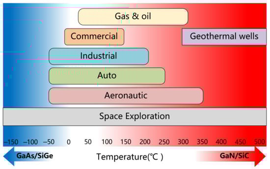
Figure 1.
Temperature ranges for different electronics applications.
Researchers represented by Oucair published a series of papers in the 1980s on the changes in electrical characteristic indicators such as the threshold voltage, leakage source current, and carrier mobility of MOS field-effect transistors in the ambient temperature range of 25 °C to 300 °C [15,16], and proposed the classic Zero-Temperature Coefficient (ZTC) bias voltage theory [17,18], providing a theoretical basis for integrated circuit design in high-temperature ranges. Since the turn of the century, on the one hand, the theory and practice of integrated circuit design in the high-temperature range have been further developed, and on the other hand, the application and development of SiC materials have provided a good solution for the design of high-temperature integrated circuits, because SiC devices have excellent thermal stability and extremely low leakage current in high-temperature environments [19,20,21,22]. Research has shown that amplification circuits designed based on SiC technology can still exhibit good performance even in extremely high-temperature environments of 400 °C, which is incomparable to classical semiconductor materials such as Si, GaAs, SiGe, etc. [23,24,25]. However, the development level of SiC technology is still in its early stages, with immature technology, high cost, and low yield rate restricting its widespread application. Therefore, scholars are still mainly exploring and researching the design of high-temperature integrated circuits using relatively mature semiconductor processes.
SOI CMOS technology has demonstrated enhanced temperature capability, as its reduced substrate thickness enables low leakage current. SOI technology offers an effective solution for ensuring the high-temperature operation (up to 250 °C) of instrumentation amplifiers. Extensive research has been conducted on the performance and temperature compensation techniques of SOI CMOS devices, as well as other challenges associated with circuit operation at elevated temperatures [26,27,28,29,30]. Furthermore, a variety of fundamental circuit modules have been successfully implemented using SOI CMOS technology [31,32,33,34,35].
In recent years, design strategies for low-noise amplifiers (LNAs) operating over high-temperature ranges have been broadly categorized into two approaches. The first involves employing the classic ZTC voltage bias technique, where the gate voltage of the MOS transistor is biased at the ZTC point to mitigate the temperature dependence of the LNA’s performance. While this method can reduce temperature-related variations to some extent, not all transistors within the same process exhibit a well-defined and convergent ZTC point. Moreover, in many cases, locating such a point is challenging, limiting the effectiveness of this approach. The second approach dynamically compensates for temperature-induced changes in transistor characteristics by generating bias currents or voltages proportional to temperature. This method offers greater adaptability but is sensitive to manufacturing variations, which can compromise the accuracy of the compensation and, consequently, the performance of the amplifier. Both of these mainstream solutions provide the partial stabilization of gain and noise performance during temperature variations, but they remain constrained by inherent limitations. Therefore, further research is required to develop improved and optimized techniques that enable LNAs to function reliably over broader temperature ranges while maintaining stable performance metrics across varying thermal conditions.
The remainder of this article is organized as follows. Section 2 reviews the issues related to the design of low-offset operational amplifiers in high-temperature environments. Section 3 provides a detailed description of the implemented circuit. Section 4 presents the measurement results of the proposed operational amplifier. Finally, Section 5 concludes the paper.
2. Low-Offset Operational Amplifier
Common techniques for improving accuracy include tuning, automatic zeroing, and chopper techniques. Among these, tuning techniques can only suppress the initial offset and do not address the dynamic suppression of offset. In contrast, chopping and auto-zeroing are the two most widely used dynamic misalignment suppression techniques [36,37,38,39], and they will be discussed in detail in the following sections.
2.1. Chopping
Chopping stabilization technology is a modulation technique used to mitigate the impact of defects in operational amplifiers, including noise and offset voltage. With advancements in integrated circuit technology, choppers can be efficiently implemented on chips. Chopping operates by modulating the input signal, noise, and offset voltage to different frequencies, followed by low-pass filtering to produce a signal with reduced nonlinearity.
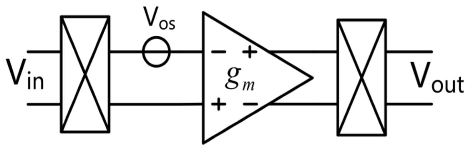
The simplified structure of the chopper amplifier is shown in Figure 2. The typical chopper amplifier consists of a chopper, amplifier, and demodulator. Among them, the input signal is modulated by the first chopper to the odd harmonic frequency of the chopping frequency. The amplifier amplifies the offset voltage, noise, and input signal, and then modulates it back to the initial frequency by the second chopper. The offset voltage Vos and noise Vn of the operational amplifier are only modulated to the chopping frequency by the output chopper and filtered by subsequent filters, thereby achieving the separation of the input signal Vin from the offset voltage and noise.

Figure 2.
The structure of the chopper amplifier.
However, this method may introduce significant ripple. Several techniques are commonly employed to mitigate this ripple. One approach is to add a low-pass filter at the amplifier’s output; however, this reduces the available signal bandwidth. A second method involves using a multi-path amplifier topology, known as chopper stabilization, although this technique increases low-frequency noise. The third method incorporates a notch filter into the amplifier. A switched-capacitor notch filter can be synchronized with the chopper clock to filter out the ripple. This type of notch filter creates notches in the amplifier’s transfer function at the chopping frequency and its odd harmonics, which can be effectively mitigated through a multi-path topology.
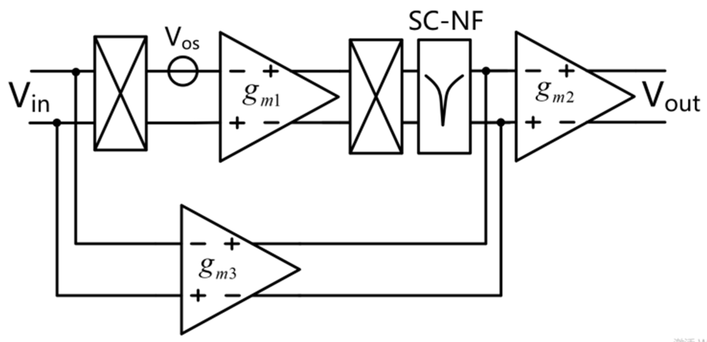
The notch filter depicted in Figure 3 suppresses ripple by incorporating a switched-capacitor notch filter (SC-NF) after the output chopper. This amplifier builds upon the classic chopper amplifier design by adding a notch filter and two amplifiers, thereby enhancing its ability to resist interference, particularly in suppressing noise and common-mode disturbances. Unlike low-pass filters, the SC-NF selectively filters out ripples near the chopping frequency, leaving low-frequency signals unaffected. As a result, this method does not impact the overall bandwidth of the operational amplifier. The use of a notch filter is particularly efficient, as the switched-capacitor network does not consume any bias current.
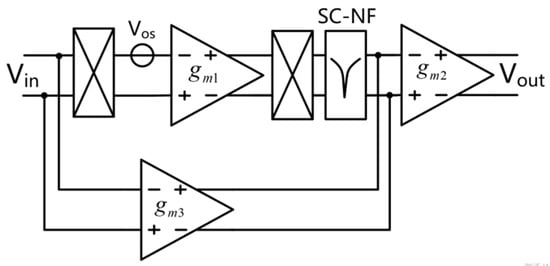
Figure 3.
Chopper amplifier with SC notch filter.
2.2. Auto-Zeroing
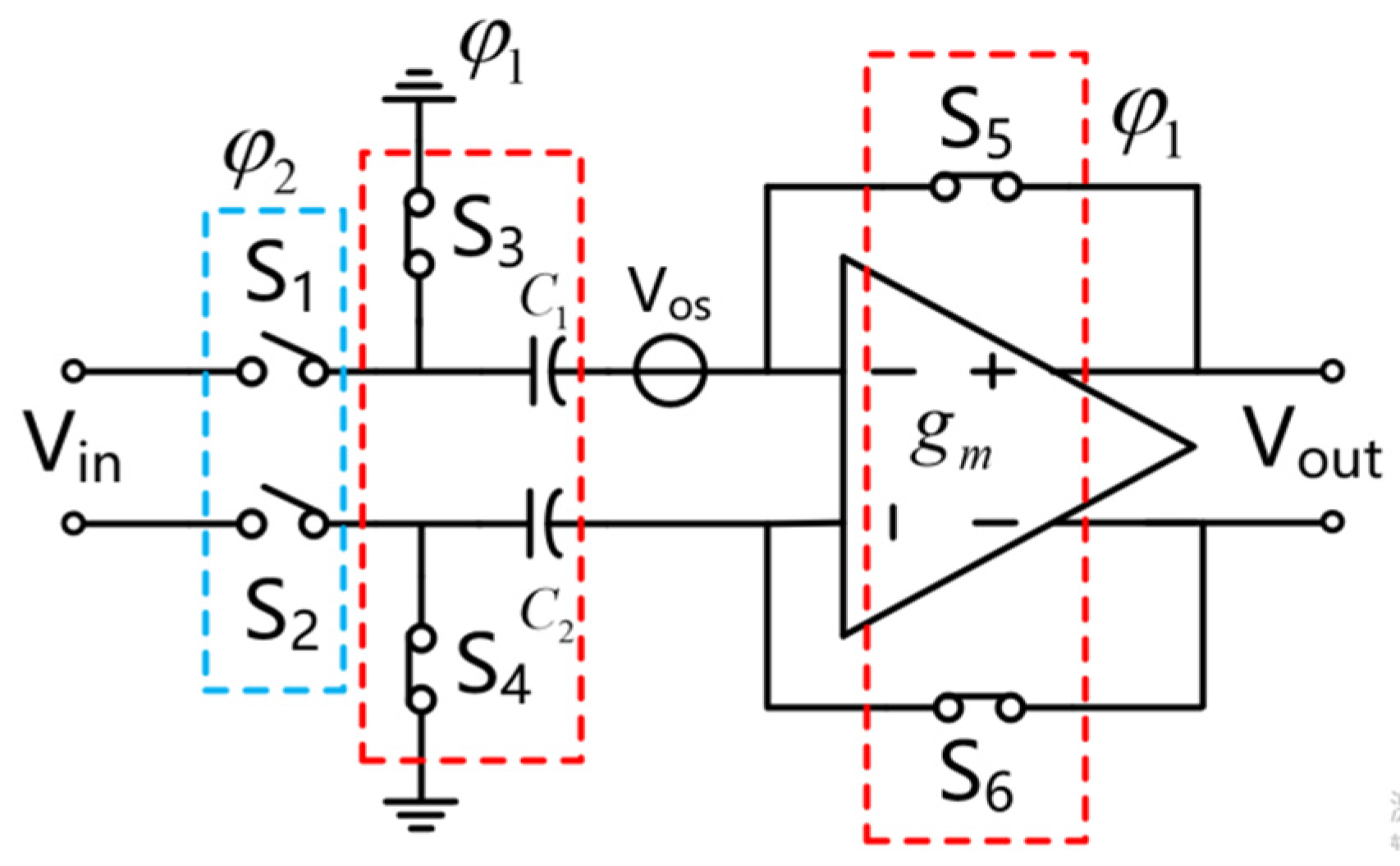
Auto-zeroing technology is a sample and hold technique that can dynamically suppress the offset voltage, noise, and temperature drift in circuits. Automatic zeroing technology stores the sampled DC offset and noise in the sampling capacitor through sampling, and then subtracts it from the signal carrying DC offset and noise, ultimately achieving the goal of suppressing DC offset and noise. The basic principle of automatic zeroing is shown in Figure 4, which is controlled by a digital clock to sample switches S1–S6, and capacitors C1 and C2 are built around an operational amplifier gm.
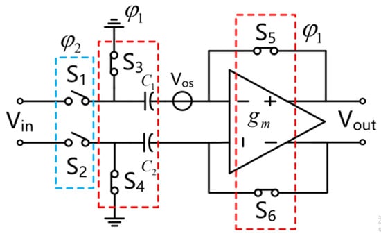
Figure 4.
Auto-zeroing diagram.
Clocks φ1 and φ2 are complementary clocks, and the method of eliminating misalignment is usually carried out in two stages. The first stage is detection and storage. When the first clock phase φ1 is at a high level, switches S1 and S2 are open, switches S3–S6 are closed, and gm is connected in a unity gain configuration. The offset voltage of the amplifier is stored in capacitor C1, as shown in (1).
The second stage is the amplification stage, in which the next clock phase φ2 is at a high level. The amplifier gm amplifies the input signal, which is then amplified by capacitors C1 and C2 before being further amplified by the amplifier. As shown in (2), the offset voltage Vos cancels out the voltage stored in capacitor C1. At this time, the input offset voltage of the amplifier is shown in (3), and the output only changes with the input differential voltage, not affected by the input offset voltage, thereby eliminating the offset voltage. Similarly, low-frequency flicker noise components are also stored on capacitors C1 and C2, and therefore will be canceled out. However, the correlation between higher-frequency flicker noise components is small, so it cannot be effectively canceled out.
Additionally, according to the sampling theorem, the sampling process can induce high-frequency thermal noise outside the desired bandwidth to mix with in-band noise. This interaction increases the noise power spectral density (PSD) within the band, resulting in a higher in-band PSD compared to the original noise floor. The noise suppression effect of automatic zeroing technology is illustrated in Figure 5. As shown, under automatic zeroing conditions, low-frequency noise is primarily flicker noise, while in the absence of automatic zeroing, low-frequency noise is predominantly white noise. However, noise aliasing leads to an increase in the spectral density of baseband noise.

Figure 5.
Noise spectrum before and after auto-zeroing.
Automatic zeroing technology offers a larger bandwidth and smaller ripple in the output voltage but comes with increased current consumption and a higher susceptibility to signal superposition, which results in elevated low-frequency noise. In contrast, chopping technology is less prone to signal superposition, but it has a narrower bandwidth, higher energy consumption, and significant output ripple at the chopping frequency. However, chopping technology generally requires lower power consumption. A comparison between the two technologies is presented in Table 1.

Table 1.
Comparison between chopping and auto-zeroing.
3. Proposed Circuit Implementation
In the standard CMOS process, devices are isolated by reverse-biased PN junctions. As the temperature increases, the current through the reverse-biased PN junction grows exponentially, leading to a significant increase in leakage current. In contrast, in the SOI process, devices are isolated by silicon dioxide insulating dielectrics, which substantially reduce leakage current and help prevent latch-up. Therefore, the circuit in this chapter is designed using the SOI process.
Although SOI process devices exhibit smaller leakage currents and a better suppression of latch-up, the electron mobility and threshold voltage of MOS devices still vary with temperature. This results in a reduction in parameters such as drain current and transconductance as temperature increases. To ensure circuit stability, the same input-stage structure and bias current are maintained across each amplifier stage. This approach ensures that, when the temperature changes, the input-stage transconductance of each stage undergoes nearly identical variations, thereby preserving overall frequency stability.
Additionally, the input stage operates in constant current mode. In the weak inversion region, where the current is low, the change in transconductance is primarily influenced by leakage current, leading to significant temperature-induced variation. In the strong inversion region, the change in transconductance is mainly driven by electron mobility, but the variation is considerably smaller than in the weak inversion region. To counteract the drop in input stage transconductance at high temperatures, a Proportional-To-Absolute-Temperature (PTAT) current source is employed, which mitigates the temperature effects and helps maintain overall frequency stability.
3.1. MNMC and Frequency Compensation Method
The circuit adopts a multipath nested Miller compensation op-amp circuit structure, which consists of a low-speed channel composed of gm1, gm2 and gm3 op amp, a chopper modulation circuit, and a notch filter in the blue area, as well as an NMC (nested Miller compensation) op amp and a high-speed channel SMC (single Miller compensation) op amp composed of gm3 and gm4. When the input signal is at a low frequency, the overall gain is mainly provided by the low-speed channel. At high frequencies, the gain is mainly provided by the high-speed channel. The overall circuit structure is shown in Figure 6.
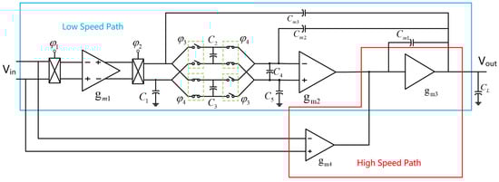
Figure 6.
Overall circuit structure composition.
The low-speed channel is actually a three-stage op amp using NMC compensation, which can be regarded as two nested two-level Miller compensation structures. The difference from the conventional NMC circuit is that the Miller capacitor of the outer loop here is divided into two parts before and after the notch filter. This design choice is based on the fact that the output signal of the post-stage notch filter lags behind the input signal by one clock cycle. By feeding back the output to the notch filter both before and after, the output waveform becomes more continuous.
The high-speed channel gm4 will produce a left-half-plane zero LHP [40]:
In order to maximize the bandwidth of the op amp, it can be used to offset the second pole of the low-speed channel NMC (z1 = p2). Finally, the third pole p3 is designed at a high frequency outside the bandwidth to increase the phase margin [40].
The main pole and the secondary main pole are located at very low frequencies, and the third pole p3 is outside the bandwidth. The final system function is similar to a two-pole system. The Bode plot will form a frequency response with a 20 dB/dec roll-off starting from the low-frequency part.
3.2. Design of Input-Stage Operational Amplifier
The input-stage op amp is a fully differential input rail-to-rail op amp. The design of the input-stage operational amplifier is shown in Figure 7. As the input-stage common-mode voltage changes from positive to negative, the input pair experiences three states: only PMOS is off, NMOS and PMOS work at the same time, and only NMOS is off. In this process, the input-stage transconductance change curve is a bell-shaped curve, the maximum value is twice the minimum value, and the frequency response curve is also the same. This requires good frequency compensation, and it is necessary to pay attention to the transient distortion caused by the fast-changing common-mode voltage modulating the input-stage transconductance.
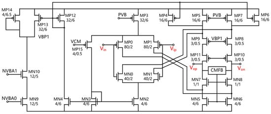
Figure 7.
Input-stage operational amplifier circuit.
To overcome the above problems, the input-stage differential pair circuit of the op amp adopts tail current control technology. By using current-switch MP15, as well as current-mirror MN2 and MN3 to provide bias for the input NMOS differential pair, the total current of the NMOS and PMOS differential pairs is a constant value. In this way, when the common-mode voltage is high and the PMOS differential pair is off, the current generated by the current source MP1 can still make the NMOS work. When the common-mode voltage is less than the reference level, the input-stage differential pair is dominated by PMOS. When the common-mode voltage is equal to the reference level, the NMOS and PMOS differential pairs work simultaneously. At this time, the input-stage transconductance is the largest, which is times that of NMOS or PMOS working alone, reducing the influence of the common-mode voltage on the input-stage transconductance [41].
The NMOS differential input pair features two common-gate stages, while the PMOS differential input pair has only one common-gate stage. This design choice is primarily aimed at increasing the output impedance. To prevent significant variation in the overall gain with changes in the input common-mode voltage, a common-gate gate voltage adjustment circuit is also incorporated. This circuit ensures that the VBP1 voltage increases as the input common-mode voltage rises, thereby adjusting the intrinsic gain of transistors MP8 and MP9.
3.3. Notch Filter
In order to reduce the output noise, on the one hand, the chopper-stabilized circuit will transfer the output noise PSD from low frequency to high frequency. The chopping frequency of the op amp should be higher than the noise corner frequency. On the other hand, it is necessary to add an LPF in the post-stage of the chopper-stabilized op amp to weaken the noise at high frequency and the higher harmonics caused by chopping.
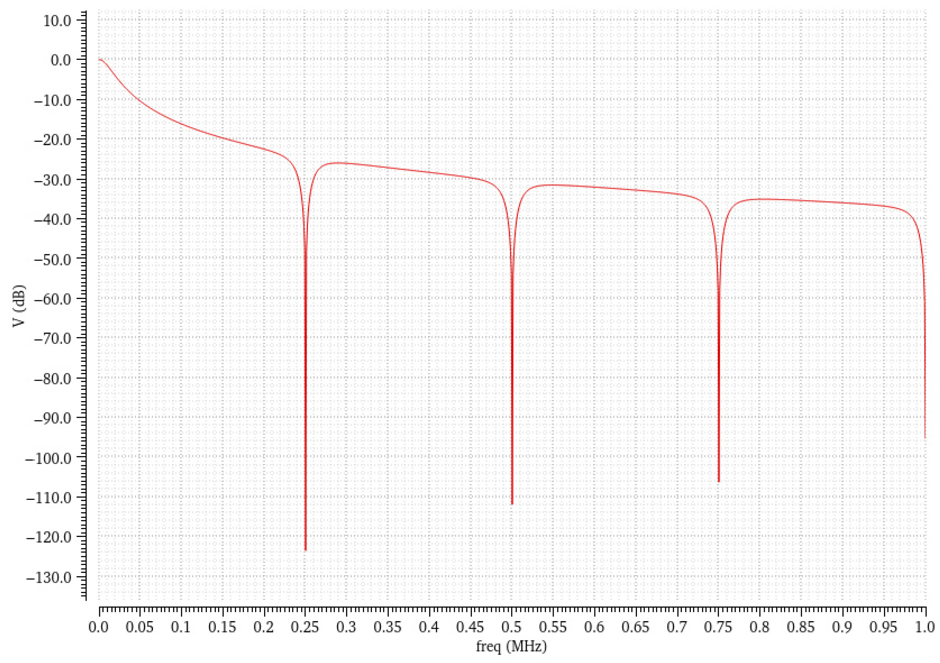
As shown in Figure 8, the circuit consists of two sampling circuits and an adder [42]. During the φ1 period, the capacitor C1B samples the input signal Vin and transfers the charge from C1A to C2; during the φ2 period, the capacitor C1A samples the input signal Vin and transfers the charge from C1B to C2. The charge after such a cycle is the sum of the two transferred charges. The overall circuit is actually equivalent to a sample-and-hold circuit, so the frequency response of the notch filter is a SINC function, and the gain is close to 0 when the input frequency is an even multiple of the chopping frequency. The spectrum of the notch filter is shown in Figure 9. In order to filter the periodic spike signals caused by the front-end chopper switch, the notch filter’s stop frequency needs to be the same as the chopper frequency, and the clock of the switch in the notch filter needs to be delayed by T/4 cycles compared to the clock of the chopper switch to avoid the influence of spike pulses.
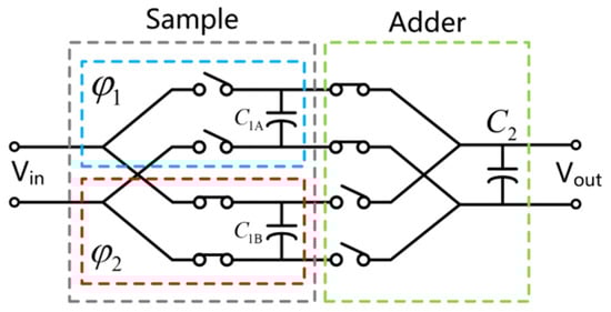
Figure 8.
The notch filter circuit.

Figure 9.
The spectrum of the notch filter.
3.4. Post-Stage Amplifier
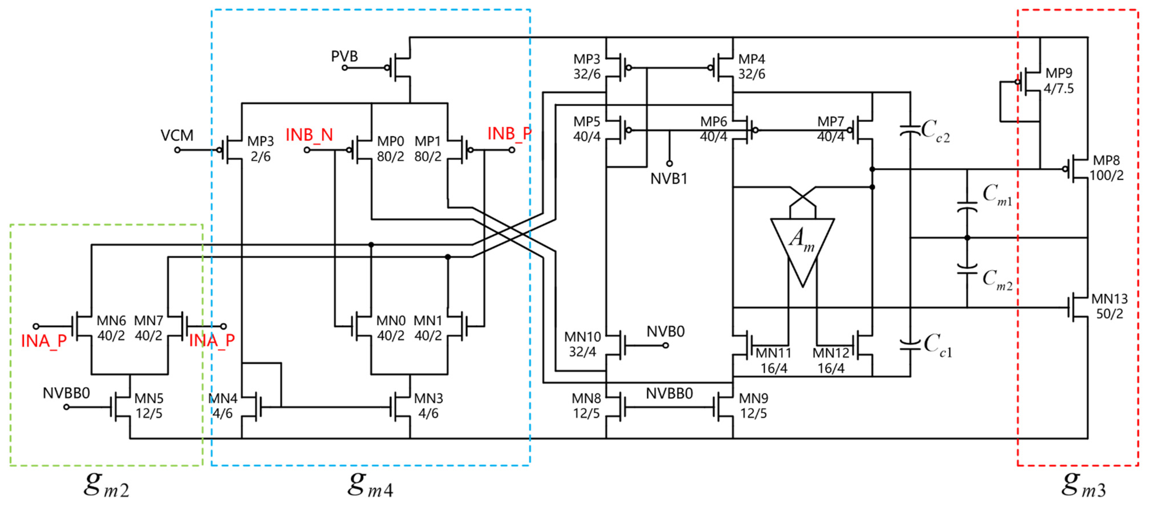
In the overall circuit, gm2 and gm4 form a current summing circuit, so in the actual circuit, the two are designed in the same op amp. As shown in Figure 10, the circuit consists of an input rail-to-rail differential pair gm4, an NMOS differential pair gm2, a Class-AB output stage circuit gm3, Miller compensation capacitors, common source, common-gate stage compensation, and a Class-AB drive circuit.
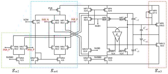
Figure 10.
Post-stage operational amplifier circuit.
3.5. Class-AB Output and Drive Circuit
In order to maintain a balance between low static power consumption and high gain when the Class-AB output circuit is working, a fixed voltage difference is required between the NMOS and PMOS gates. In a static state, a smaller voltage can be maintained between Vgsn and Vgsp, which not only reduces static power consumption but also helps to increase output impedance and thus increase gain. In a dynamic state, the small signals of Vgsn and Vgsp are completely inverted, and gmn and gmp have opposite trends.
The gain of Class-AB is
where
In order to maintain a fixed voltage difference between the NMOS and PMOS gates, a differential difference amplifier (DDA) and MN11 and MN12 are designed in the circuit to form a Class-AB drive circuit [43].
Compared with the fully differential op amp, the differential op amp adds a pair of differential pairs, which can realize such operations.
The differential operational amplifier is connected to transistors MN11 and MN12 to form a regulated cascode structure. The difference between the drain voltages of MN11 and MN12, detected by the DDA, is compared to a reference voltage and output to the gate of the transistors, forming a negative feedback loop that stabilizes the drain DC voltage. This negative feedback also reduces the gain of the common-gate stage involving MN11 and MN12, which in turn reduces the overall gain of the op amp.
In the circuit, gm2 and gm3 constitute a two-stage op amp. Miller compensation will produce a right-half-plane zero due to the existence of a feedforward signal path, reducing the phase margin and response speed of the op amp [44]. Cascode compensation does not have a feedforward path, and the response speed is greatly increased, but cascode compensation will produce a complex plane pole. When the capacitance is large, a gain spike may be generated at the pole position, reducing the gain margin of the op amp. This design uses cascode compensation and Miller compensation at the same time, which weakens the influence of the feedforward signal path of Miller compensation and increases the response speed of the op amp.
4. Measurement Results
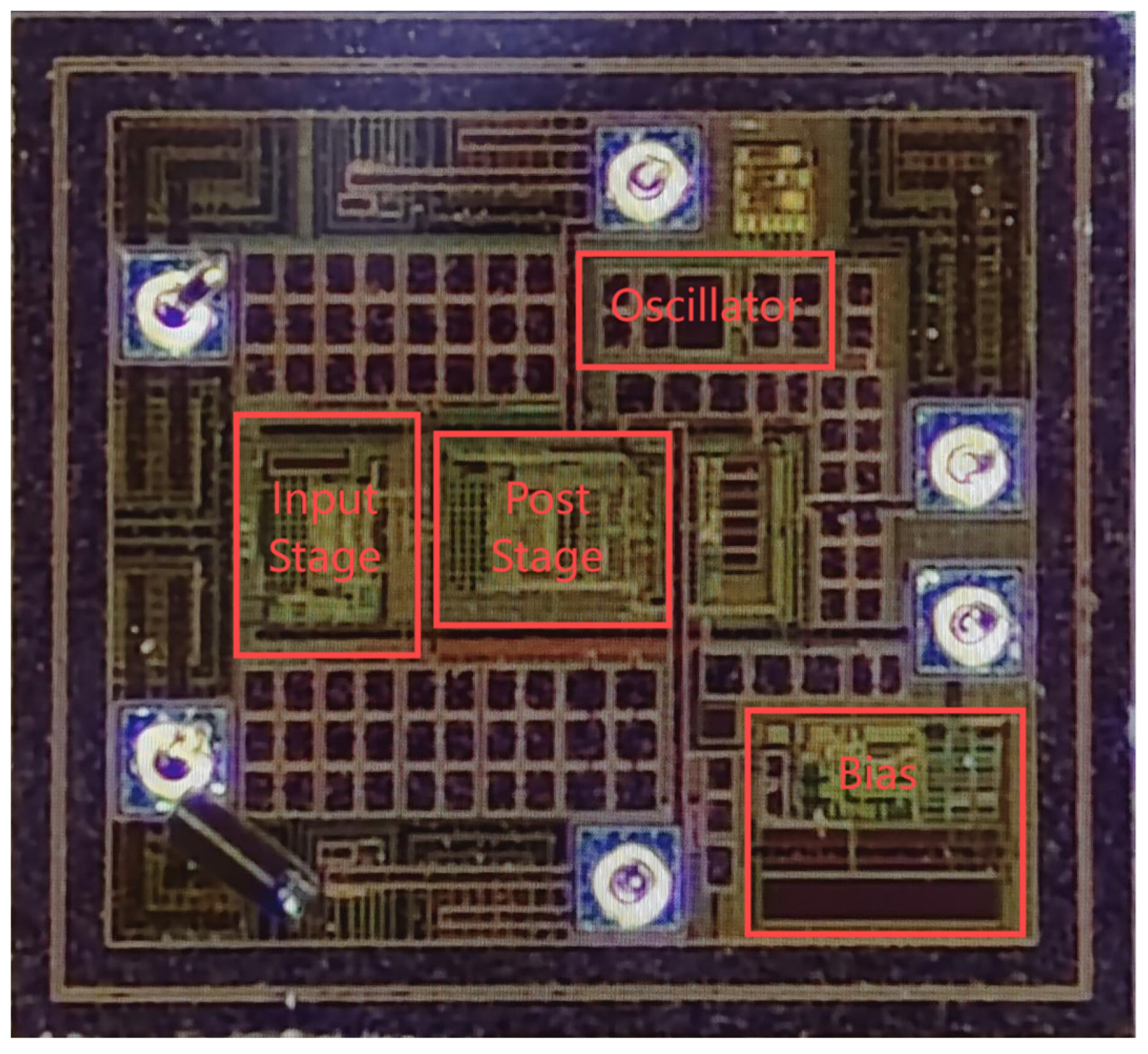
The prototype op amp is fabricated in a 0.15-µm SOI Bipolar-CMOS-DMOS (BCD) technology and its micrograph is shown in Figure 11. The total chip area is approximately 800 μm × 950 μm. It consumes 0.3 mA current from a 5 V supply.

Figure 11.
The chip micrograph.
The operational amplifier designed in this paper works at −40 °C to 250 °C. Conventional bulk silicon CMOS devices face serious leakage and threshold voltage Vth drift problems at high temperatures, especially above 125 °C. The SOI process can solve the leakage problem due to its natural structural characteristics. Combined with the interconnection process and special doping treatment, it can effectively solve the problem of threshold voltage Vth drift with temperature.
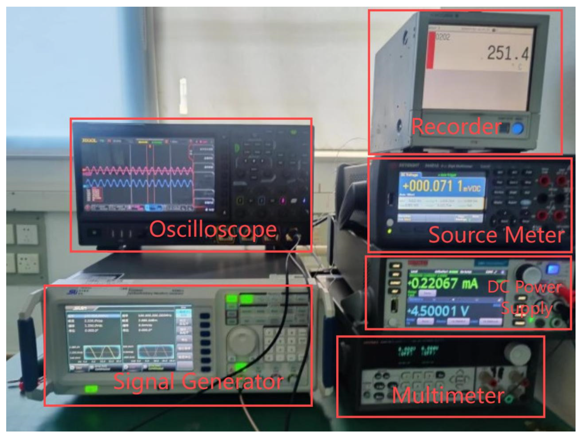
The measurement setup used to characterize the performance of the op amp is shown in Figure 12. The system was tested across a wide temperature range from −40 °C to 250 °C to evaluate its robustness and stability under extreme operating conditions. The results from this extensive temperature range are crucial for assessing the performance and reliability of the amplifier in high-temperature environments, as detailed in the following sections.

Figure 12.
Measurement setup.
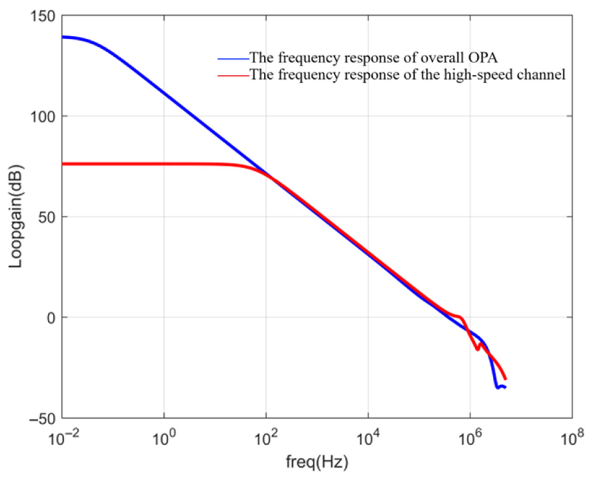
The frequency response of the operational amplifier was first evaluated with a 100 pF load capacitor at 250 °C, and the resulting open-loop gain is depicted in Figure 13. The blue curve represents the overall frequency response of the operational amplifier, while the red curve represents the frequency response of the high-speed channel. As shown, the low-frequency gain is primarily determined by the low-speed channel, while at higher frequencies, the gain of the high-speed channel dominates, coinciding with the overall gain. At this point, the overall gain is predominantly governed by the high-speed channel. The maximum open-loop gain at low frequencies reaches 140 dB. However, due to the overall frequency response rolling off with a slope of 40 dB per decade, the gain–bandwidth product (GBW) is approximately 100 kHz. This performance highlights the effectiveness of the multi-path hybrid nested Miller compensation, which enables stable operation over a wide range of frequencies while maintaining a high gain at low frequencies.

Figure 13.
Open-loop gain (with a 100 pF load capacitor at 250 °C).
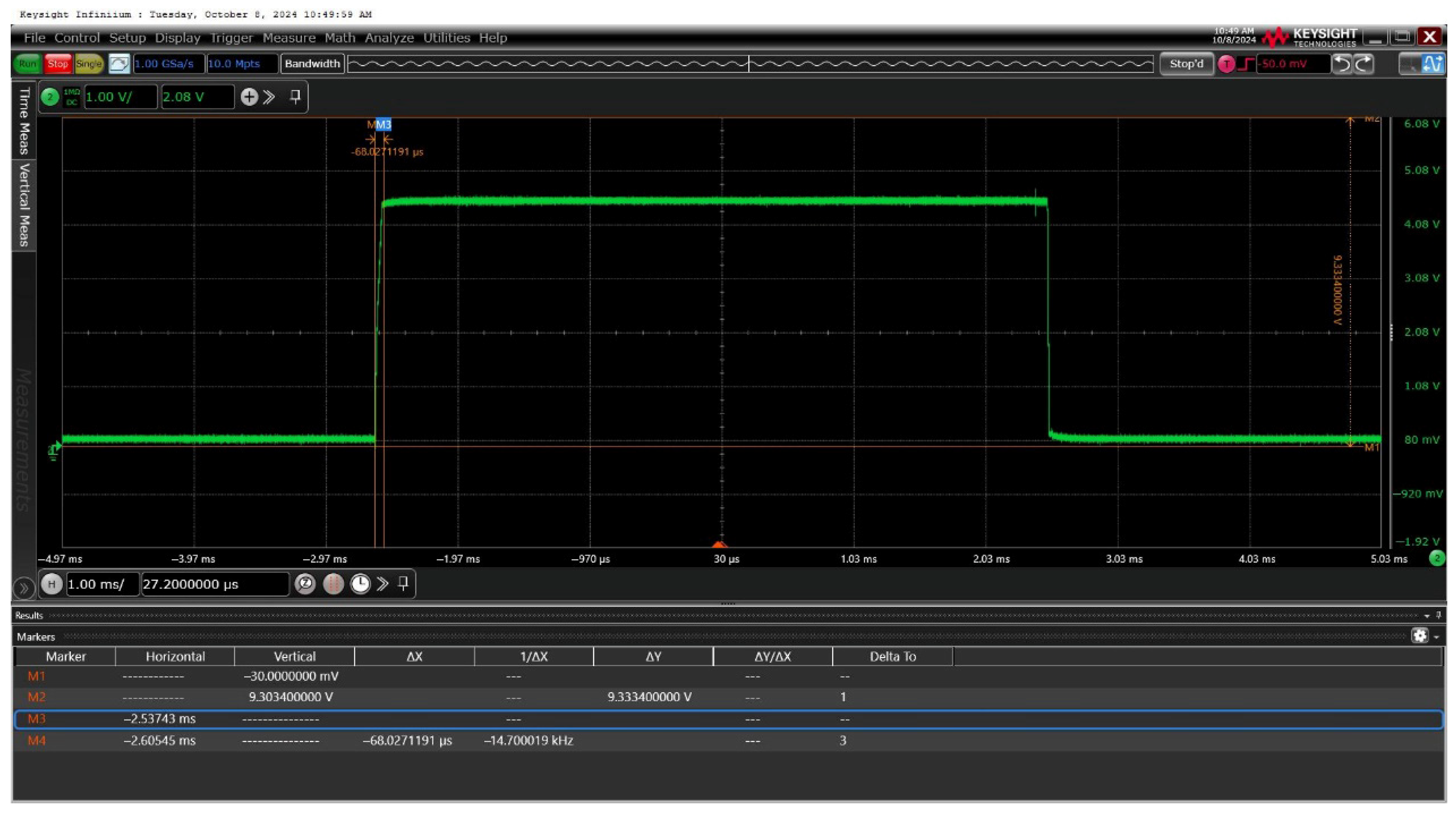
In a subsequent test, the op amp was configured as a unity-gain buffer, and the small-signal frequency response was measured using a 5 V step input signal with a cycle time of 10 ms. The results of this test are shown in Figure 14. This configuration demonstrates the op amp’s ability to maintain linearity and stability in response to a rapid input signal transition, further validating its performance under varying operating conditions.
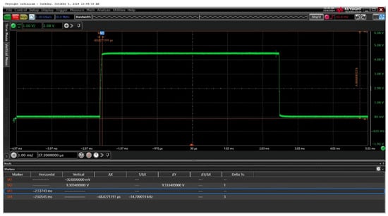
Figure 14.
Pulse response (with a 5 V step input signal with a cycle time of 10 ms).
Table 2 summarizes the important parameter test results of the chip at room temperature. It can be seen that under a static current of 0.3 mA, both an offset voltage of 20 μV and a GBW of 0.1 MHz are ensured, as well as 140 dB. Furthermore, the operational amplifier demonstrates rail-to-rail input and output, ensuring a wide input range and maximizing the output voltage swing.
Table 2.
Typical parameters of the amplifier at room temperature.
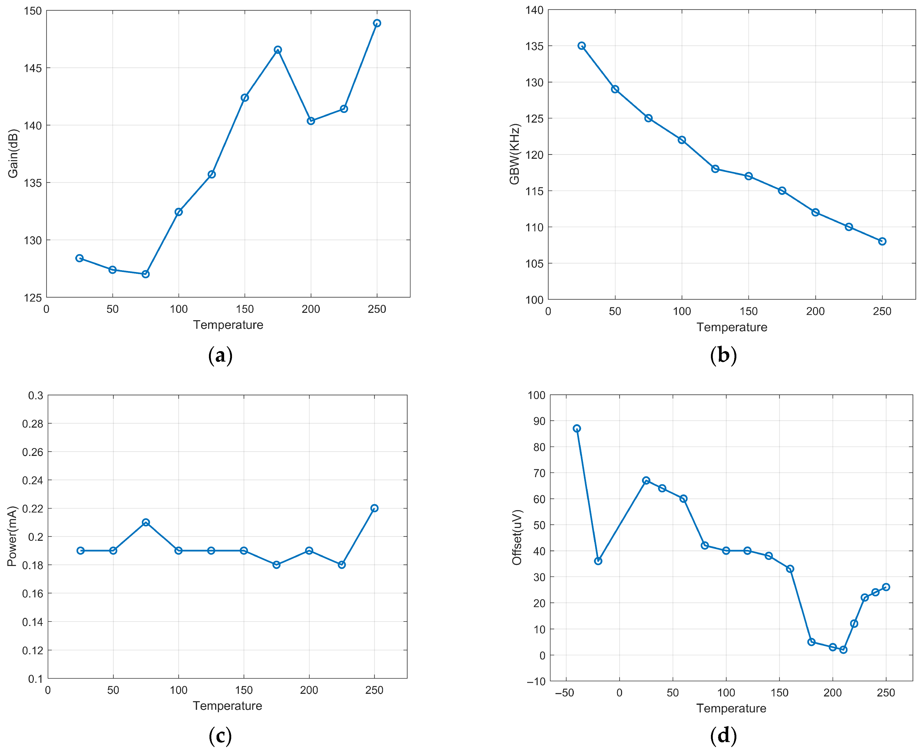
To verify the amplifier’s operation in the targeted temperature range between −40 °C and 250 °C, extensive measurements have been performed. The temperature regulation involves placing the chip into a temperature chamber, and its model is MC-811B-2. The measurement results of some key parameters of the circuit vary with temperature, as shown in Figure 15. These parameter variations indicate the circuit’s stability under temperature changes, ensuring its proper operation in high-temperature environments.
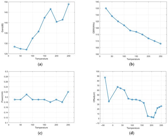
Figure 15.
Measurement results versus temperature: (a) gain; (b) GBW; (c) power; (d) offset.
Table 3 summarizes and compares the performance of the operational amplifier in high-temperature applications. As shown, the amplifier achieves an offset voltage as low as 20 µV and a high DC gain of 140 dB, demonstrating its suitability for precision applications in demanding environments. These results underscore the amplifier’s ability to maintain exceptional performance, even under extreme temperature conditions, ensuring stability and reliability across a wide operational range.
Table 3.
Comparison with previous work.
5. Conclusions
This paper presents a chopper-stabilized operational amplifier for high-temperature applications. The multipath nested Miller compensation structure, along with an SC notch filter, is proposed to reduce input offset and ripple. The amplifier has a high DC gain (140 dB) and bandwidth (100 KHz) with rail-to-rail input and output signal range. Compared with a traditionally structured op amp, this work achieves a lower offset while being more efficient in terms of power and area. The effectiveness of the proposed op amp has been demonstrated over a wide temperature range from −40 °C to 250 °C. Finally, this op amp also exhibits excellent power efficiency, input noise, and offset voltage. As a result, 20 µV offset and 0.7 μV/°C maximum drift are achieved over the rail-to-rail input range. As a result of to the above characteristics, this chip can be used in fields such as aerospace, oil and gas exploration, automotive electronics, and nuclear industry, where there is a strong demand for electronic devices to withstand high-temperature environments, such as amplifying and filtering pressure sensors, as well as temperature and humidity sensors in analog front-end application circuits.
Author Contributions
Conceptualization, Z.Y. and J.L.; methodology, J.F.; validation, J.S.; writing—original draft preparation, Z.Y.; writing—review and editing, Z.Y. and Q.C.; visualization, J.F.; supervision, S.Q.; project administration, S.Q. All authors have read and agreed to the published version of the manuscript.
Funding
This work was supported in part by the National Key Research and Development Program of China under Grant 2021YFB3202704.
Institutional Review Board Statement
Not applicable.
Informed Consent Statement
Not applicable.
Data Availability Statement
The data provided in this study are available upon request from the corresponding author. The data are not available to the public due to the confidentiality of the related R&D products.
Conflicts of Interest
The authors declare no conflicts of interest.
References
- Pathrose, J.; Liu, C.; Chai, K.; Xu, Y. A Time-Domain Band-Gap Temperature Sensor in SOI CMOS for High-Temperature Applications. IEEE Trans. Circuits Syst. II Express Briefs 2015, 62, 436–440. [Google Scholar] [CrossRef]
- Pour, F.L.; Ha, D. A Temperature Compensated 5 GHz GaN on SiC Power Amplifier. In Proceedings of the 2020 63rd International Midwest Symposium on Circuits and Systems (MWSCAS), Springfield, MA, USA, 9–12 August 2020; pp. 549–553. [Google Scholar]
- Wang, Q.; Li, M.; Niu, X.; Liu, M.; Wang, B. Model and Design of High-Temperature Ultrasonic Sensors for Detecting Position and Temperature Based on Iron-Based Magnetostrictive Wires. IEEE Sens. J. 2021, 21, 26868–26877. [Google Scholar] [CrossRef]
- Madhusoodhanan, S.; Sandoval, S.; Zhao, Y.; Ware, M.E.; Chen, Z. A Highly Linear Temperature Sensor Using GaN-on-SiC Heterojunction Diode for High Power Applications. IEEE Electron Device Lett. 2017, 38, 1105–1108. [Google Scholar] [CrossRef]
- Lu, X.; Wang, L.; Yang, Q.; Yang, F.; Gan, Y.; Zhang, H. Investigation and Comparison of Temperature-Sensitive Electrical Parameters of SiC mosfet at Extremely High Temperatures. IEEE Trans. Power Electron. 2023, 38, 9660–9672. [Google Scholar] [CrossRef]
- Elgabra, H.; Singh, S. High Temperature Simulation of 4H-SiC Bipolar Circuits. IEEE J. Electron Devices Soc. 2015, 3, 302–305. [Google Scholar] [CrossRef]
- Cunningham, M.L.; Ha, D.S.; Koh, K.J. A high temperature wideband low noise amplifier for downhole applications. In Proceedings of the 2016 IEEE International Symposium on Circuits and Systems (ISCAS), Montreal, QC, Canada, 22–25 May 2016; pp. 938–941. [Google Scholar]
- Fang, L.; Gui, P. A Low-Noise Low-Power Chopper Instrumentation Amplifier With Robust Technique for Mitigating Chopping Ripples. IEEE J. Solid-State Circuits 2022, 57, 1800–1811. [Google Scholar] [CrossRef]
- Lin, T.N.; Wang, B.; Bermak, A. Ripple Suppression in Capacitive-Gain Chopper Instrumentation Amplifier Using Amplifier Slicing. IEEE Trans. Circuits Syst. I Regul. Pap. 2021, 68, 3991–4000. [Google Scholar] [CrossRef]
- Kim, H.; Han, K.; Kim, J.; You, D.; Heo, H.; Kwon, Y. Chopper-Stabilized Low-Noise Multipath Operational Amplifier With Dual Ripple Rejection Loops. IEEE Trans. Circuits Syst. II Express Briefs 2020, 67, 2427–2431. [Google Scholar] [CrossRef]
- Zheng, H.; Ding, Y.; Liu, X. A 0.04 mm2/Channel Neural Amplifier with An Input-Referred Noise of 4.6 µVrms and Power Consumption of 3 µW. In Proceedings of the 2024 IEEE International Symposium on Circuits and Systems (ISCAS), Singapore, 19–22 May 2024; pp. 1–5. [Google Scholar]
- Falina, S.; Kawarada, H.; Manaf, A.A.; Syamsul, M. High Temperature Performance of Enhanced Endurance Hydrogen Terminated Transparent Polycrystalline Diamond FET. IEEE Electron. Dev. Lett. 2022, 43, 1101–1104. [Google Scholar] [CrossRef]
- Shaddock, D.; Yin, L. High temperature electronics packaging: An overview of substrates for high temperature. In Proceedings of the 2015 IEEE International Symposium on Circuits and Systems (ISCAS), Lisbon, Portugal, 24–27 May 2015; pp. 1166–1169. [Google Scholar]
- Sbrana, C.; Catania, A.; Paliy, M.; Pascoli, S.D.; Strangio, S.; Macucci, M. Design Criteria of High-Temperature Integrated Circuits Using Standard SOI CMOS Process up to 300 °C. IEEE Access 2024, 12, 57236–57249. [Google Scholar] [CrossRef]
- Shoucair, F.S.; Ojala, P.K. High-temperature electrical characteristics of GaAs MESFETs (25–400 degrees C). IEEE Trans. Electron Devices 1992, 39, 1551–1557. [Google Scholar] [CrossRef]
- Shoucair, F.S. High-temperature latchup characteristics in VLSI CMOS circuits. IEEE Trans. Electron Devices 1988, 35, 2424–2426. [Google Scholar] [CrossRef]
- Catapano, E.; Frutuoso, T.M.; Cassé, M.; Ghibaudo, G. On the Zero Temperature Coefficient in Cryogenic FD-SOI MOSFETs. IEEE Trans. Electron Devices 2023, 70, 845–849. [Google Scholar] [CrossRef]
- Salamin, S.; Van Santen, V.M.; Rapp, M.; Henkel, J.; Amrouch, H. Minimizing Excess Timing Guard Banding Under Transistor Self-Heating Through Biasing at Zero-Temperature Coefficient. IEEE Access 2021, 9, 30687–30697. [Google Scholar] [CrossRef]
- Chiah, S.B.; Zhou, X.; Yuan, L. Compact Zero-Temperature Coefficient Modeling Approach for MOSFETs Based on Unified Regional Modeling of Surface Potential. IEEE Trans. Electron Devices 2013, 60, 2164–2170. [Google Scholar] [CrossRef]
- Bose, A.; Biswas, D.; Hishiki, S.; Ouchi, S.; Kitahara, K.; Kawamura, K.; Wakejima, A. A Temperature Stable Amplifier Characteristics of AlGaN/GaN HEMTs on 3C-SiC/Si. IEEE Access 2021, 9, 57046–57053. [Google Scholar] [CrossRef]
- Choi, P.H.; Kim, Y.P.; Park, S.; Hong, S.M.; Lee, S.; Lee, H.; Jang, J.H. High-Temperature Annealing of High Purity Semi-Insulating 4H-SiC and Its Effect on the Performance of a Photoconductive Semiconductor Switch. IEEE Electron Dev. Lett. 2023, 44, 1168–1171. [Google Scholar] [CrossRef]
- Gu, Z.; Yang, M.; Yang, Y.; Liu, X.; Gao, M.; Qi, J.; Liu, W.; Han, C.; Geng, L.; Hao, Y. Comparative Study on High-Temperature Electrical Properties of 1.2 kV SiC MOSFET and JBS-Integrated MOSFET. IEEE Trans. Power Electron. 2024, 39, 4187–4420. [Google Scholar] [CrossRef]
- Hedayati, R.; Lanni, L.; Rusu, A.; Zetterling, C.M. Wide temperature range integrated amplifier in bipolar 4H-SiC technology. In Proceedings of the 2016 46th European Solid-State Device Research Conference (ESSDERC), Lausanne, Switzerland, 12–15 September 2016; pp. 198–201. [Google Scholar]
- Tian, Y.; Lanni, L.; Rusu, A.; Zetterling, C.M. Silicon Carbide Fully Differential Amplifier Characterized Up to 500 °C. IEEE Trans. Electron Devices 2016, 63, 2242–2247. [Google Scholar] [CrossRef]
- Hedayati, R.; Lanni, L.; Rodriguez, S.; Malm, B.G.; Rusu, A.; Zetterling, C.M. A Monolithic, 500 °C Operational Amplifier in 4H-SiC Bipolar Technology. IEEE Electron Dev. Lett. 2014, 35, 693–695. [Google Scholar] [CrossRef]
- Balashov, E.V.; Ivanov, N.V.; Korotkov, A.S. SOI Instrumentation Amplifier for High-Temperature Applications. In Proceedings of the 2020 IEEE East-West Design & Test Symposium (EWDTS), Varna, Bulgaria, 4–7 September 2020; pp. 1–4. [Google Scholar]
- Zhang, X.; Liu, F.; Li, B.; Yang, C.; Huang, Y.; Lu, P.; Chen, S.; Cheng, J.; Wang, Q.; Yu, A.; et al. Comparison of Total Ionizing Dose Effects in SOI FinFETs Between Room and High Temperature. IEEE Trans. Nucl. Sci. 2022, 69, 359–366. [Google Scholar] [CrossRef]
- Omprakash, A.P.; Dao, H.; Raghunathan, U.S.; Ying, H.; Chakraborty, P.S.; Babcock, J.A.; Mukhopadhyay, R.; Cressler, J.D. An Investigation of High-Temperature (to 300 °C) Safe-Operating-Area in a High-Voltage Complementary SiGe on SOI Technology. IEEE Trans. Electron Devices 2017, 64, 3748–3755. [Google Scholar] [CrossRef]
- Halder, A.; Nyssens, L.; Vanbrabant, M.; Rack, M.; Lederer, D.; Kilchytska, V.; Raskin, J.P. Impact of High Temperature Up to 175 °C on the DC and RF Performances of 22-nm FD-SOI MOSFETs. IEEE Trans. Electron Devices 2023, 70, 4987–4992. [Google Scholar] [CrossRef]
- Mehta, H.; Kaur, H. Study on Impact of Parasitic Capacitance on Performance of Graded Channel Negative Capacitance SOI FET at High Temperature. IEEE Trans. Electron Devices 2019, 7, 2904–2909. [Google Scholar] [CrossRef]
- Gimenez, S.P.; Galembeck, E.H.S.; Renaux, C.; Flandre, D. Impact of Using the Octagonal Layout for SOI MOSFETs in a High-Temperature Environment. IEEE Trans. Device Mater. Reliab. 2015, 15, 626–628. [Google Scholar] [CrossRef]
- Analog Devices. High Temperature, Low Power Operational Amplifier. AD9634 Datasheet. Available online: https://www.analog.com/media/en/technical-documentation/data-sheets/AD9634.pdf (accessed on 15 September 2015).
- Le Ba, N.; Kim, T. Design of Temperature-Aware Low-Voltage 8T SRAM in SOI Technology for High-Temperature Operation (25 %C–300 %C). IEEE Trans. Very Large Scale Integr. (VLSI) Syst. 2017, 25, 2383–2387. [Google Scholar] [CrossRef]
- Cochet, M.; Keller, B.; Clerc, S.; Abouzeid, F.; Cathelin, A.; Autran, J.L.; Roche, P.; Nikolić, B. A 225 μm Probe Single-Point Calibration Digital Temperature Sensor Using Body-Bias Adjustment in 28 nm FD-SOI CMOS. IEEE Solid-State Circuits Lett. 2018, 1, 14–17. [Google Scholar] [CrossRef]
- Wang, Z.; Shi, X.; Tolbert, L.M.; Wang, F.; Liang, Z.; Costinett, D.; Blalock, B.J. A high temperature silicon carbide mosfet power module with integrated silicon-on-insulator-based gate drive. IEEE Trans. Power Electron. 2015, 30, 1432–1445. [Google Scholar] [CrossRef]
- Safiallah, M.; Danesh, A.R.; Pu, H.; Heydari, P. A Current-Adjusting Auto-Zeroing Technique for DC-Offset and Flicker-Noise Cancellation. IEEE Trans. Very Large Scale Integr. (VLSI) Syst. 2023, 31, 1950–1959. [Google Scholar] [CrossRef]
- Chen, K.; Li, D.; Chen, D.; Chai, C. An Improved MOS Self-Biased Ring Amplifier and Modified Auto-Zeroing Scheme. IEEE Trans. Very Large Scale Integr. (VLSI) Syst. 2023, 31, 606–610. [Google Scholar] [CrossRef]
- Fang, L.; Gui, P. A 14nV/√Hz 14μW Chopper Instrumentation Amplifier with Dynamic Offset Zeroing (DOZ) Technique for Ripple Reduction. In Proceedings of the 2019 IEEE Custom Integrated Circuits Conference (CICC), Austin, TX, USA, 14–17 April 2019; pp. 1–4. [Google Scholar]
- Qu, T.; Pan, Q.; Liu, L.; Zeng, X.; Hong, Z.; Xu, J. A 1.8–GΩ Input-Impedance 0.15–μV Input-Referred–Ripple Chopper Amplifier With Local Positive Feedback and SAR-Assisted Ripple Reduction. IEEE J. Solid-State Circuits 2023, 58, 796–805. [Google Scholar] [CrossRef]
- Leung, K.N.; Mok, P.K. Analysis of multistage amplifier-frequency compensation. IEEE Trans. Circuits Syst. I Fundam. Theory Appl. 2001, 48, 1041–1056. [Google Scholar] [CrossRef]
- Huijsing, J. Operational Amplifiers Theory and Design; Springer: Cham, Switzerland, 2017; ISBN 978-3-31-928126-1/978-3-31-928127-8. [Google Scholar]
- Bilotti, A.; Monreal, G. Chopper-stabilized amplifiers with a track-and-hold signal demodulator. IEEE Trans. Circuits Syst. I Fundam. Theory Appl. 1999, 46, 490–495. [Google Scholar] [CrossRef]
- Sackinger, E.; Guggenbuhl, W. A versatile building block: The CMOS differential difference amplifier. IEEE J. Solid-State Circuits 1987, 22, 287–294. [Google Scholar] [CrossRef]
- Yavari, M.; Shoaei, O.; Svelto, F. Hybrid cascode compensation for two-stage CMOS operational amplifiers. In Proceedings of the 2005 IEEE International Symposium on Circuits and Systems, Kobe, Japan, 23–26 May 2005; Volume 2, pp. 1565–1568. [Google Scholar] [CrossRef]

Disclaimer/Publisher’s Note: The statements, opinions and data contained in all publications are solely those of the individual author(s) and contributor(s) and not of MDPI and/or the editor(s). MDPI and/or the editor(s) disclaim responsibility for any injury to people or property resulting from any ideas, methods, instructions or products referred to in the content. |
© 2025 by the authors. Licensee MDPI, Basel, Switzerland. This article is an open access article distributed under the terms and conditions of the Creative Commons Attribution (CC BY) license (https://creativecommons.org/licenses/by/4.0/).