Article

Enhanced Control Strategy for Three-Level T-Type Converters in Hybrid Power-to-X Systems

by
Moria Sassonker Elkayam
* and
Dmitri Vinnikov
Department of Electrical Power Engineering and Mechatronics, Tallinn University of Technology, 19086 Tallinn, Estonia
*
Author to whom correspondence should be addressed.
Appl. Sci. 2025, 15(5), 2409; https://doi.org/10.3390/app15052409
Submission received: 19 January 2025 / Revised: 16 February 2025 / Accepted: 18 February 2025 / Published: 24 February 2025
(This article belongs to the Special Issue Control of Power Systems II)

Abstract

:
This paper presents a dual-loop control system designed for three-level three-phase T-type converters, optimizing their performance in the hybrid operation of Power-to-X systems. Due to the increasing of distributed power generation based on renewable energy sources, Power-to-X systems convert surplus renewable energy into other forms of energy, such as hydrogen, synthetic fuels, or chemical storage, which can be stored and later converted back to electricity or used in other applications. Bidirectional converters play a crucial role in hybrid system operation, which requires an efficient and reliable power conversion to maintain stability and performance. The proposed dual-loop control system includes an inner current loop for fast current regulation and an outer voltage loop to maintain stable voltage levels, ensuring precise control of the output of the converter and enhancing its response to dynamic changes in load and generation. Additionally, the control system incorporates a technique to balance the split DC-link capacitors voltages, a major challenge in three-level converters. Comprehensive simulation and experimental results demonstrate the efficacy of the proposed control system in maintaining high power quality and supporting the hybrid operation of Power-to-X systems.

1. Introduction

The transition to sustainable energy systems is driving the integration of renewable energy sources and advanced energy storage technologies into the power grid. Power-to-X (P2X) systems, which convert surplus electrical energy into various forms of storable energy, such as hydrogen, synthetic fuels, or other valuable chemicals, play a crucial role in this transformation [1,2,3,4,5,6]. It enables the storage and utilization of renewable energy in various sectors, contributing to a more sustainable energy system. In a Power-to-hydrogen (P2H) system, excess renewable generation is utilized to produce hydrogen, which can then be stored in a hydrogen storage tank. This stored hydrogen can later be converted back into electricity using fuel cells to meet the electricity demand through converters, as shown in Figure 1, also known as the hydrogen-to-power (H2P) process [7,8,9]. Designing a reliable P2X process that uses renewable energy and grid electricity as backup power is challenging due to the uncertain nature of renewables and potential limits on grid usage. Bidirectional DC-to-AC or AC-to-DC converters play a fundamental role in managing power flows in hybrid systems, such as shown in Figure 1, ensuring compatibility between the different energy forms and maintaining the stability and reliability of the power grid [3,10,11]. Different bidirectional topologies such as T-type, neutral point clamped (NPC), and active neutral point clamped (ANPC) have evolved rapidly in such high power and high voltage hybrid systems [12,13,14]. Among these, T-type converters have been chosen in this paper due to their lower conduction losses, reduced complexity, and improved efficiency compared to NPC and ANPC topologies. NPC converters, while effective at balancing capacitor voltages, suffer from higher conduction losses and increased component count. ANPC converters offer additional control flexibility but introduce higher switching losses and complexity in implementation. T-type converters provide an optimal balance between efficiency, implementation feasibility, and performance in P2X applications, making them the preferred choice for this paper [15,16]. DC-to-AC converters (also known as inverters) are used in the integration of batteries and fuel cells in P2X systems, which enhances the flexibility and resilience of energy management [17]. Batteries offer rapid response capabilities and high efficiency for short-term energy storage, while fuel cells provide long-term storage solutions and high energy density. In addition, inverters are a key component in renewable energy integration to hybrid systems such as photovoltaic systems connected to the grid [11,18,19]. The need for this research arises from the growing challenge of maintaining power quality and system stability in hybrid P2X energy conversion systems. Current methods, as detailed in the Literature Survey section that follows, suffer from steady-state errors, limited adaptability to grid disturbances, and inefficient power flow management. To address these limitations, this study develops a novel dual-loop control strategy that improves system robustness, enhances power quality, and ensures precise tracking of reference signals. This approach is essential for enabling more efficient and reliable integration of renewable energy into the power grid.

2. Literature Survey

For the hybrid system to receive instantaneous power, sinusoidal current and voltage need to be injected, and the controller must track or compensate for these sinusoidal signals [20,21,22]. Traditionally, proportional-integral (PI) control in the synchronous reference frame has been used to achieve zero steady-state tracking error. However, this approach often exhibits steady-state errors in both amplitude and phase when managing AC signals [1,23,24]. These issues have been mitigated with stationary frame resonant compensators [25,26,27,28]. These compensators, single-resonant or multi-resonant, provide exceptionally high gain at specific non-zero frequencies, distinguishing them from classical stationary frame PI controllers and effectively minimizing steady-state errors to near-zero levels [29,30,31,32]. This paper proposes a novel dual-loop control configuration for three-level three-phase T-type converters. Existing dual-loop control frameworks typically incorporate an inner current loop and an outer voltage loop, but their ability to handle disturbances efficiently varies significantly. Traditional implementations rely heavily on PI-based controllers, which struggle to maintain robust performance under dynamic grid conditions. Our proposed control strategy builds upon these frameworks by incorporating a novel feed-forward (FF) action that enhances disturbance rejection, improves transient response, and ensures more stable voltage regulation compared to conventional methods. The FF action is implemented within the inner loop to preemptively cancel disturbances before they propagate through the system. Unlike traditional feedback-based disturbance rejection, which reacts only after a disturbance has impacted system performance, the FF action proactively mitigates its effects by adjusting control inputs in real time. This approach significantly improves system robustness, particularly under fluctuating grid conditions and load variations [33,34].
The proposed dual-loop control configuration in this paper includes an inner loop containing a two-degrees-of-freedom control structure, i.e., (a) inner loop of FF action to cancel disturbances and (b) an outer loop of tracking controller for inverter output current which injected into the grid or to an AC load through an LC or LCL filter, and the outer loop of the dual-loop control structure contains tracking controller for the capacitor voltage (output voltage in case of an LC filtered inverter). Since the disturbances are cancelled by the FF action, the control problem of both outer loops reduces to imposing tracking behavior. Hence, the control strategy of the tracking controllers is based on the time-domain design of a single-resonant controller [35,36]. In addition, the proposed design considers actuator delay present in any practical system and the bandwidth limitation resulting from the two-degree-of-freedom inner loop by considering the closed loop transfer function of the inner loop when designing the controller of the outer loop. Another critical aspect is the balancing of DC voltage capacitors, a task that becomes increasingly complex in three-level T-Type converters due to their inherent topology [37,38]. Unlike two-level converters, whose DC link is usually implemented using a single capacitor, three-level converters employ split DC links; thus, their control structures must contain two DC link voltages in order to regulate the sum and the difference of partial DC link voltages. This paper introduces a control strategy to address the imbalance problem alongside the implementation of the dual-loop control setup.
This paper is structured as follows: In Section 2, three-phase three-level bidirectional AC-to-DC and DC-to-AC converter structures are introduced, as well as their role in P2X systems. Section 3 presents the proposed control structure with detailed analysis, including the DC link capacitors’ voltage balancing. Finally, Section 4 presents simulation and experimental results to validate the proposed methodology.

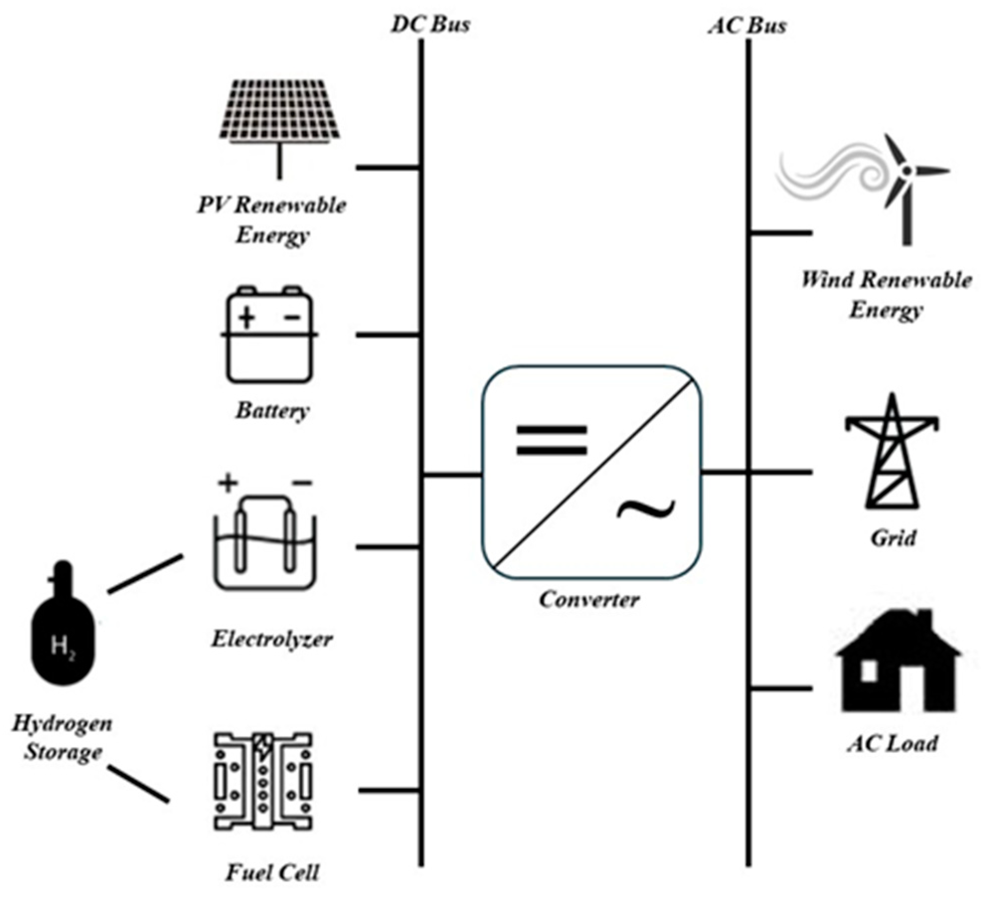
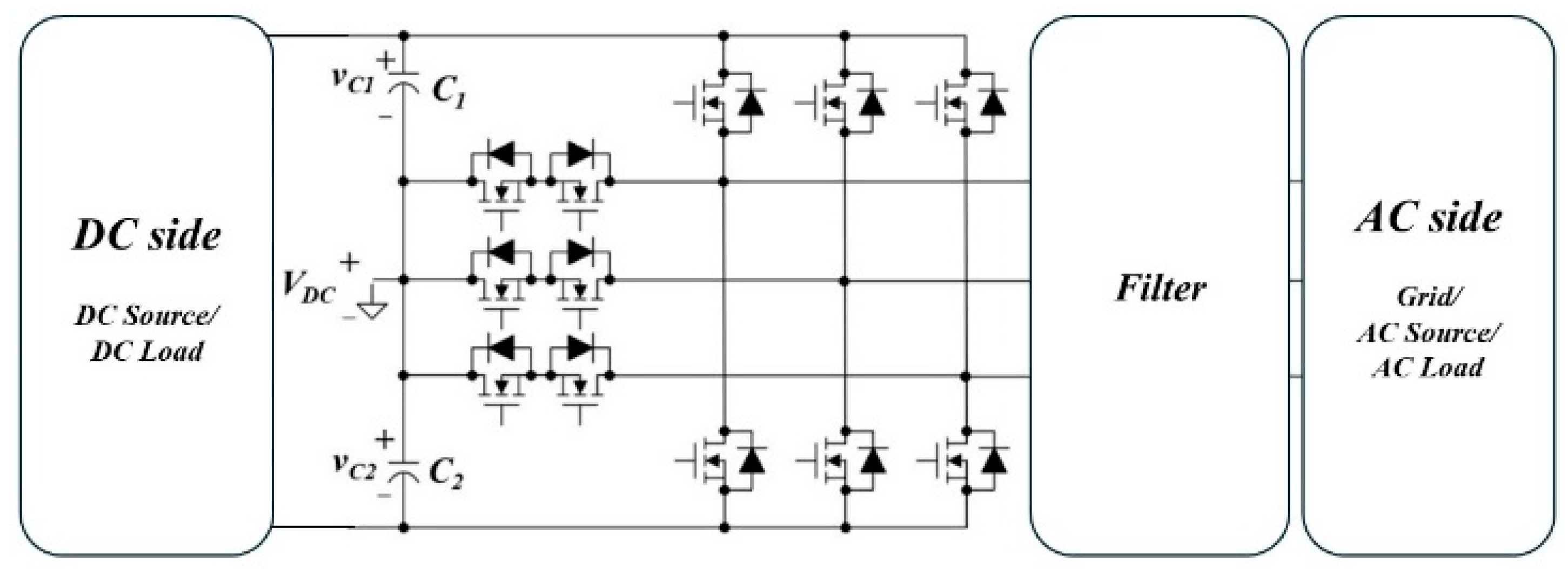
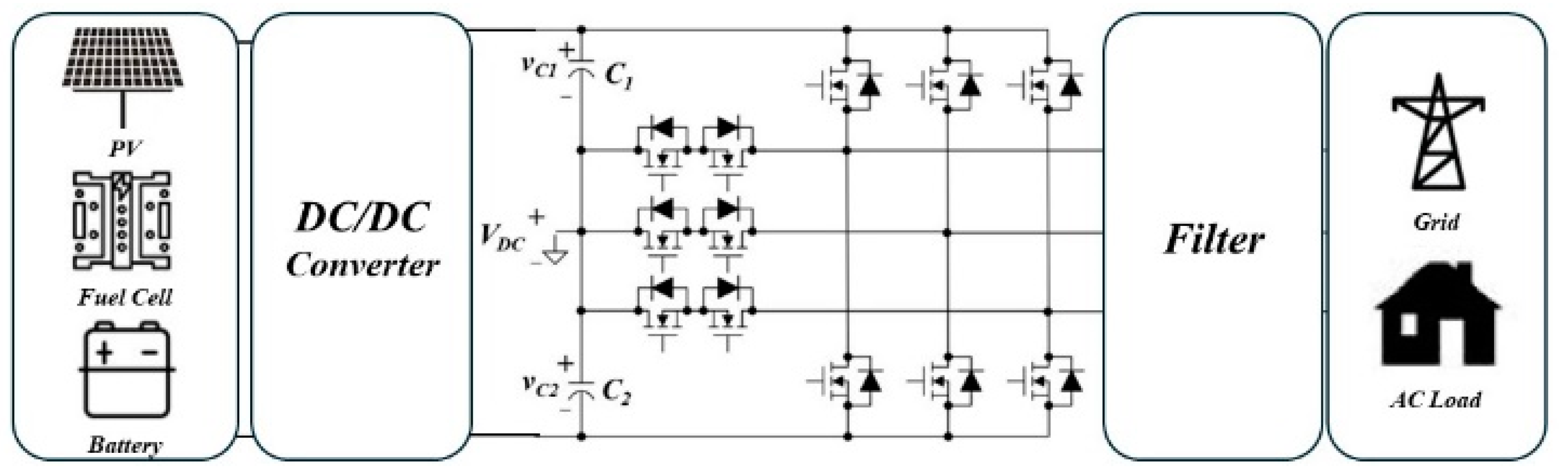
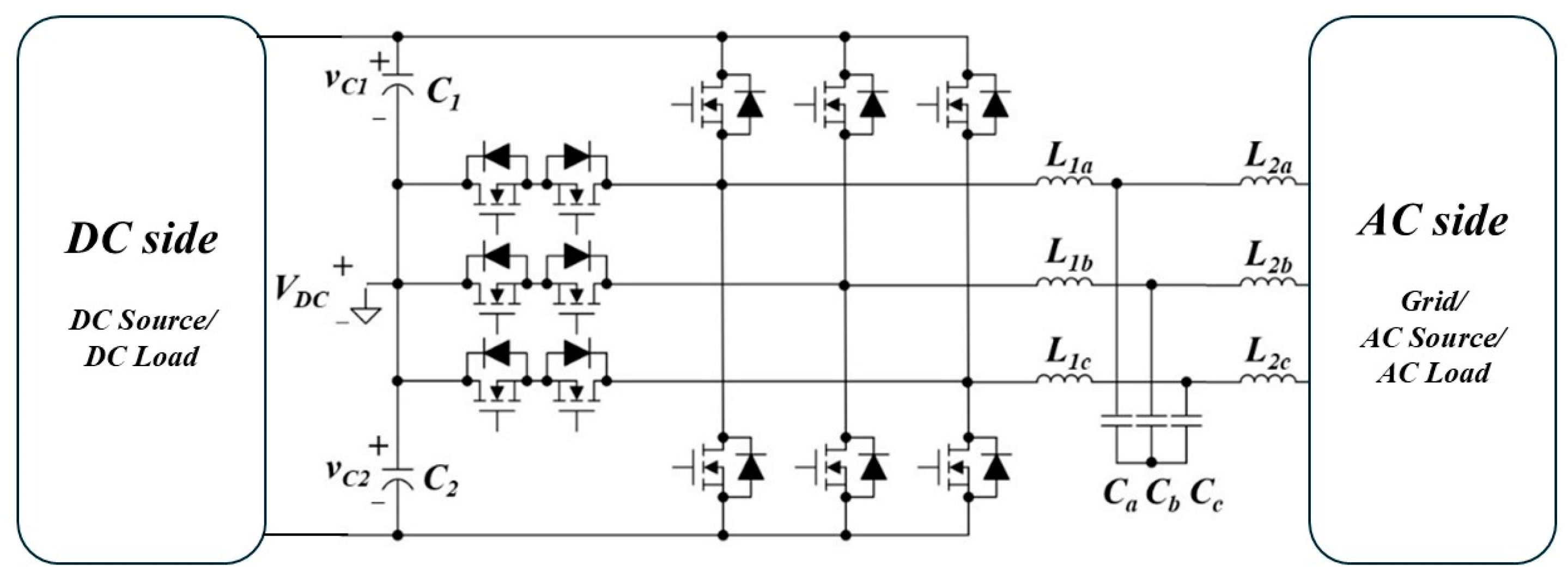
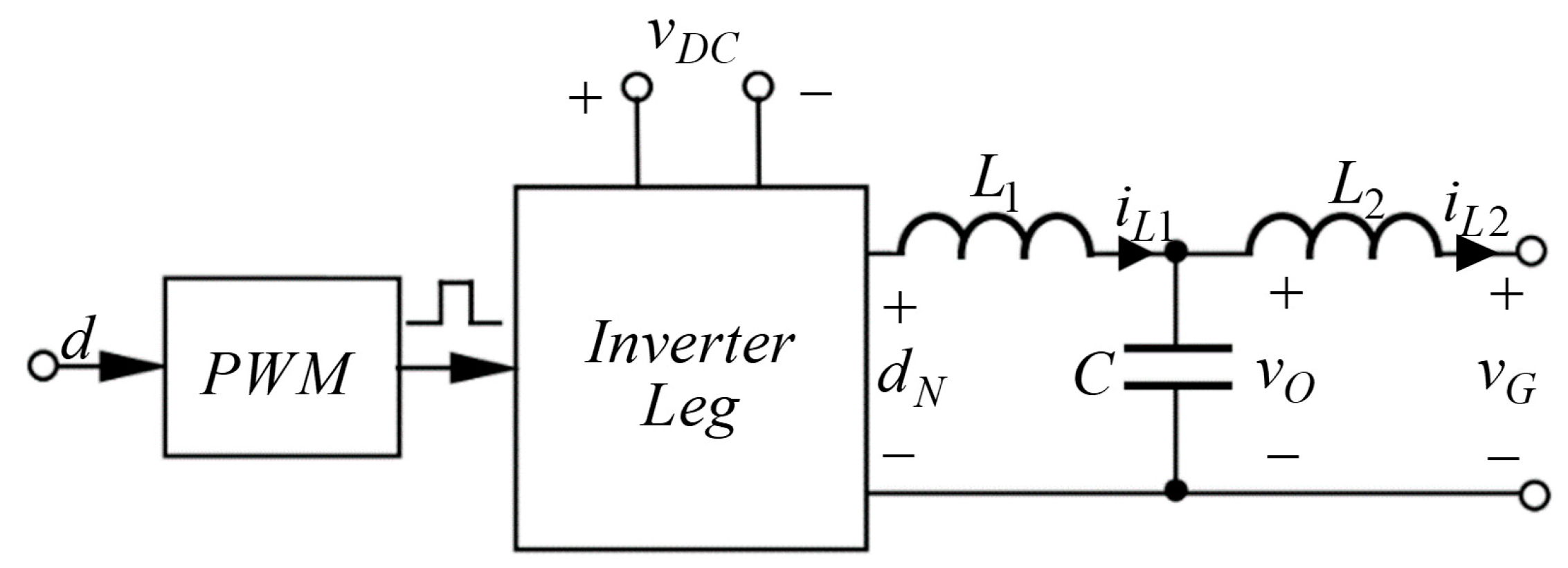
3. Three-Phase T-Type Bidirectional Converter

Bidirectional multilevel converters are a combination of DC voltage sources/DC loads and switching power electronic components (IGBT, SiC MOSFET, etc.) connected to an AC loads/AC source through filter, L or LC or LCL filter, as shown in Figure 2, where a three-phase T-type converter is employed. Bidirectional multilevel converters play a significant role in the hybrid operation of P2X systems, as shown in Figure 3. T-type, as employed in this paper, and NPC topologies are the most common of three-phase three-level converters, widely used in high power applications such as P2X (10 kVA–100 kVA).
This paper focuses on three-phase three-level T-type filtered converter which is powered by a DC voltage source VDC, representing by energy source such as PV renewable energy source, battery storage, fuel cell, which are all connected through a DC/DC converter as shown in Figure 3, or wind power connected through an AC/DC converter. The converter acts as a DC/AC converter, connected to an AC load or to the grid. Figure 4 shows LCL filter implantation for the T-type converter employed in this paper. L1x is the inverter side inductor, where x refers to the phases a, b, or c. Cx is the filter capacitor of each phase, and L2x is the grid/load side inductor of each phase. The proposed control regulates the voltage across the capacitor voltage and the current injected from the inverter to the grid or to an AC load, maintaining stable voltage levels and fast current regulation to enhance the dynamic response to changes in load and generation.
Figure 5 presents a single-phase representation of the controlled converter in order to simplify the control methodology. vO and vG represent the output voltage across the filter capacitance and the grid voltage, respectively, and d is the controller output. The inverter side inductor L1 current is iL1, and the grid/output side inductor L2 current is represented by iL2.

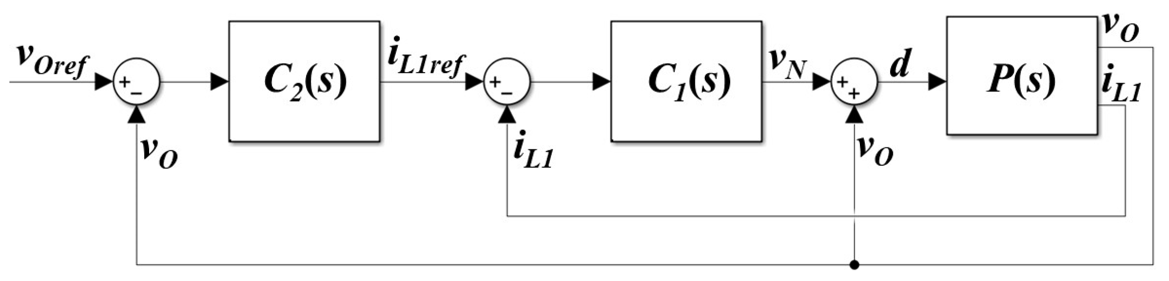
4. Proposed Control Design

The block diagram of the proposed dual-loop control system is shown in Figure 6. The controllers C1(s) and C2(s) need to be designed to ensure that the steady-state error for the inverter-side inductor current and the capacitor voltage reference tracking are minimized.

4.1. Feed-Forward Capacitor Voltage Loop

According to Figure 5, the current dynamics of the inverter-side inductor L1 are described using the following switching-period-averaged equation:
L 1 d i L 1 ( t ) d t = d ( t T d ) v D C ( t ) R 1 i L 1 ( t ) v O ( t ) ; d N ( t ) = d ( t T d ) v D C ( t )
with Td symbolizing sampling and transport delay and R1 denoting the equivalent resistance of L1. The DC-linked voltage vDC(t) is assumed constant or measurable, as shown in Figure 5. The capacitor voltage, i.e., output voltage, vO(t), is used as an FF signal to the controller in order to decouple the system dynamics from external disturbances. The control signal is then given by the following:
d ( t ) = 1 v D C ( t ) v N ( t ) + v O ( t )
where vN(t) is the current tracking controller C1(s) (Figure 6) output signal. Then, the corresponding plant transfer function may be expressed as the following:
P ( s ) = P I L 1 ( s ) / D ( s ) ( s ) = v D C R 1 + L 1 s e T d s .

4.2. Inverter Side Inductor Inner Control Loop

Since the disturbance of the current loop, i.e., the output voltage, is eliminated by the FF action, which makes the system dynamics decoupled from external disturbances, the controller C1(s) goal is to track the reference inductor current iL1(t), given by the following:
i L 1 r e f ( t ) = K I sin ω 0 t u ( t )
where KI is the current amplitude and ω0 is the grid frequency. Since the current amplitude is produced from the external loop of output voltage control, it is unknown or a requirement for executing a computationally intensive real-time Fourier transform. However, in order to decouple the controller design from the current amplitude information requirement, a control strategy based on time domain transient response of single resonant controllers is proposed. The design procedure is based on setting a closed-loop system response to a sinusoidal reference with a unit step magnitude (Equation (4)) or in the Laplace domain ([35,36]) as in the following:
I L 1 r e f ( s ) = K I ω 0 s 2 + ω 0 2 .
the time- and Laplace-domains output current are defined by
i L 1 ( t ) = K I sin ω 0 t u ( t ) 1 e ω C t ,
and
I L 1 ( s ) = K I ω 0 s 2 + ω 0 2 2 ω C I s + ω C I 2 ( s + ω C I ) 2 + ω 0 2
where ωCI−1 is the transient time constant of the current loop. Dividing (5) and (7) leads to the following closed-loop transfer function:
I L 1 r e f ( s ) I L 1 ( s ) = 2 ω C I s + ω C I 2 ( s + ω C I ) 2 + ω 0 2 .
On the other hand, the closed loop transfer function is defined by the following:
I L 1 r e f ( s ) I L 1 ( s ) = L G ( s ) 1 + L G ( s )
hence, comparing (8) and (9), the corresponding open-loop transfer function can be obtained as the following:
L G ( s ) = C ( s ) P ( s ) = 2 ω C I s + ω C I 2 s 2 + ω 0 2 ,
where the controller can then be derived accordingly as in the following:
C ( s ) = 2 ω C I s + ω C I 2 s 2 + ω 0 2 P ( s ) 1 ,
where P(s) is defined in (3). To enhance robustness against frequency variations, a damping term is incorporated into the resonant controller. While adding damping reduces the resonant peak gain, it helps mitigate frequency shifts caused by digital implementation constraints such as finite word length and quantization effects. Without damping, these factors can lead to deviations in the resonant frequency, reducing system performance. The trade-off involved is that increasing damping improves stability but slightly compromises steady-state accuracy. To counteract this, the crossover frequency should be set as high as feasible to maintain adequate control performance. This approach ensures reliable tracking and rejection of disturbances while preventing instability issues commonly associated with ideal resonators. The current controller is then defined with practical modification according to [33] as follows:
C 1 ( s ) = L 1 s + R 1 2 ω C I s + ω C I 2 s 2 + 2 ξ ω 0 s + ω 0 2
the controller coefficients L1 and R1 are known from the system plant, and the remaining controllers coefficients, i.e., resonant term bandwidth ξ and transient response frequency ωCI, have yet to be determined. In order to design the controller, loop-gain shaping, according to [29], is proposed. Loop-gain with practical modification is defined as follows:
L G ( s ) = 2 ω C I s + ω C I 2 s 2 + 2 ξ ω 0 s + ω 0 2 e T d s
or
L G ( j ω ) = ω C I 2 + j 2 ω C I ω ω 0 2 ω 2 + j 2 ξ ω 0 ω e j T d ω .
loop-gain phase and magnitude can be expressed as
L G ( ω ) = t g 1 2 ω ω C I t g 1 2 ξ ω 0 ω ω 0 2 ω 2 T d ω
and
L G ( ω ) = ω C I ( ω 0 2 ω 2 ) 2 + ( 2 ξ ω 0 ω ) 2 ω C I ω 0 2 ω C I ω 2 + 4 ξ ω 0 ω 2 2 + 2 ω ( ω 0 2 ω 2 ξ ω 0 ω C I ) 2
Let ωBI define the crossover frequency of the inner current loop, i.e., loop-gain magnitude is equal to 0 dB and the phase equal to −180° + PM, where PM is the desired phase margin to avoid system instability (typically 45°). Assuming ωBI is much higher than fundamental frequency ω0 (ω0 ~(50–60)2π rad·s−1), (15) can be defined as the following:
L G ( ω B ) = t g 1 2 ω B I ω C I t g 1 2 ξ ω 0 ω B I 0 T d ω B I = π + P M
According to [36], the relation between crossover frequency ωBI to transient response frequency ωCI is the following:
ω B I = 2.1 ω C I
Then, (17) can be rewritten as follows:
L G ( ω B I ) = t g 1 4 T d ω B I = π + P M
And transient response frequency ωCI is therefore derived as follows:
ω C I = 1.33 P M 2 T d .
The value of the resonant term bandwidth ξ is selected to achieve desired steady-state performance, namely robustness to fundamental frequency variations in the following range 0.001ω0 < ω < 0.01ω0. Then, the typical value of ξ is 0.01–0.001.
The design process adheres to the following steps:
-
Specify the target phase margin PM of the inner current loop;
-
Determine the delay value Td according to the switching frequency (Td~1.5 Ts);
-
Set the value of crossover frequency ωBI according to (18) and (20);
-
Set the value of ξ to be between 0.01–0.001;
-
Shape the controller and loop gain according to (12) and (13), respectively.
A Bode diagram of the resulting open loop transfer function of the current loop with system parameters, which is summarized in Table 1, is shown in Figure 7a. The system desired PM set to 45°, and the resulting calculated bandwidth according to (18) following the above design process is ωBI = 2π·3000 rad·s−1. It can be seen that system parameters, PM, and bandwidth correspond to calculated parameters.

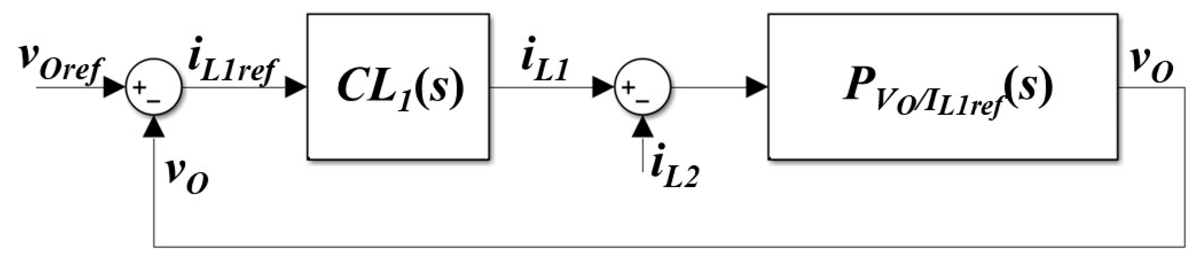
4.3. Output Voltage Outer Control Loop

The plant transfer function of the capacitor/output voltage, vO, to the inverter side inductor current, iL1, can be defined by the following:
P V O ( s ) / I L 1 r e f ( s ) ( s ) = 1 s C
which is resolved by the following dynamic equation:
i L 1 ( t ) = C d v O ( t ) d t + i L 2 ( t )
i.e., the desired reference current of the inverter side inductor current, is set by the capacitor voltage control loop as shown in Figure 6. Then, voltage controller C2(s) is defined as (11) with the plant defined in (21) and different time constant ωCV as follows:
C 2 ( s ) = s C 2 ω C V s + ω C V 2 s 2 + 2 ξ ω 0 s + ω 0 2
The bandwidth frequency of the voltage control loop is then defined as follows:
ω B V 0.5 π P M T d 2 .
In order to obtain the maximum crossover frequency of the capacitor voltage loop, the delay Td2 caused by the inner loop must be determined. Figure 8 shows the equivalent capacitor voltage loop diagram according to (21) and (22). It can be shown that the voltage loop actuator delay is the closed loop transfer function of the current loop (Equations (8) and (9)) [39] as in the following:
C L I ( s ) = I L 1 r e f ( s ) I L 1 ( s ) = 2 ω C I s + ω C I 2 ( s + ω C I ) 2 + ω 0 2 .
Combining (25) and (13), considering the switching and sampling delay and the damping factor, results in the following transfer function:
C L I ( s ) = 2 ω C I s + ω C I 2 ( s 2 + 2 ξ ω 0 s + ω 0 2 ) e T d s + 2 ω C I s + ω C I 2 .
then, the corresponding loop gain is defined as follows:
L G V ( s ) = C V ( s ) C L I ( s ) P V O / I L 1 r e f ( s ) = 2 ω C s + ω C 2 ( s 2 + 2 ξ ω 0 s + ω 0 2 ) e T d s + 2 ω C s + ω C 2 1 s C
The Bode diagram of the current closed-loop CLI(s) (Equation (26)) transfer function is shown in Figure 7b. It can be seen from the bode diagram that CLI(s) act as an actuator delay, setting the voltage loop bandwidth. Then, Td2 can be found according to Figure 7b and is twice that of Td. Then, the maximum crossover frequency of the capacitor voltage loop may be defined as the following:
ω B V 0.5 π P M 2 T d .
where the transient response frequency ωCV is derived as follows:
ω C V = 1.33 P M 4 T d .
Figure 8. Equivalent block diagram of the voltage loop.
Applsci 15 02409 g008
The design process of the outer loop adheres to the following steps:
-
Specify the target phase margin PM of the voltage loop;
-
Determine the delay value Td according to the Bode diagram of a current closed loop;
-
Set the value of crossover frequency ωBV according to (28) and (29);
-
Set the value of ξ to be between 0.01–0.001;
-
Shape the controller and loop gain according to (23) and (27), respectively.

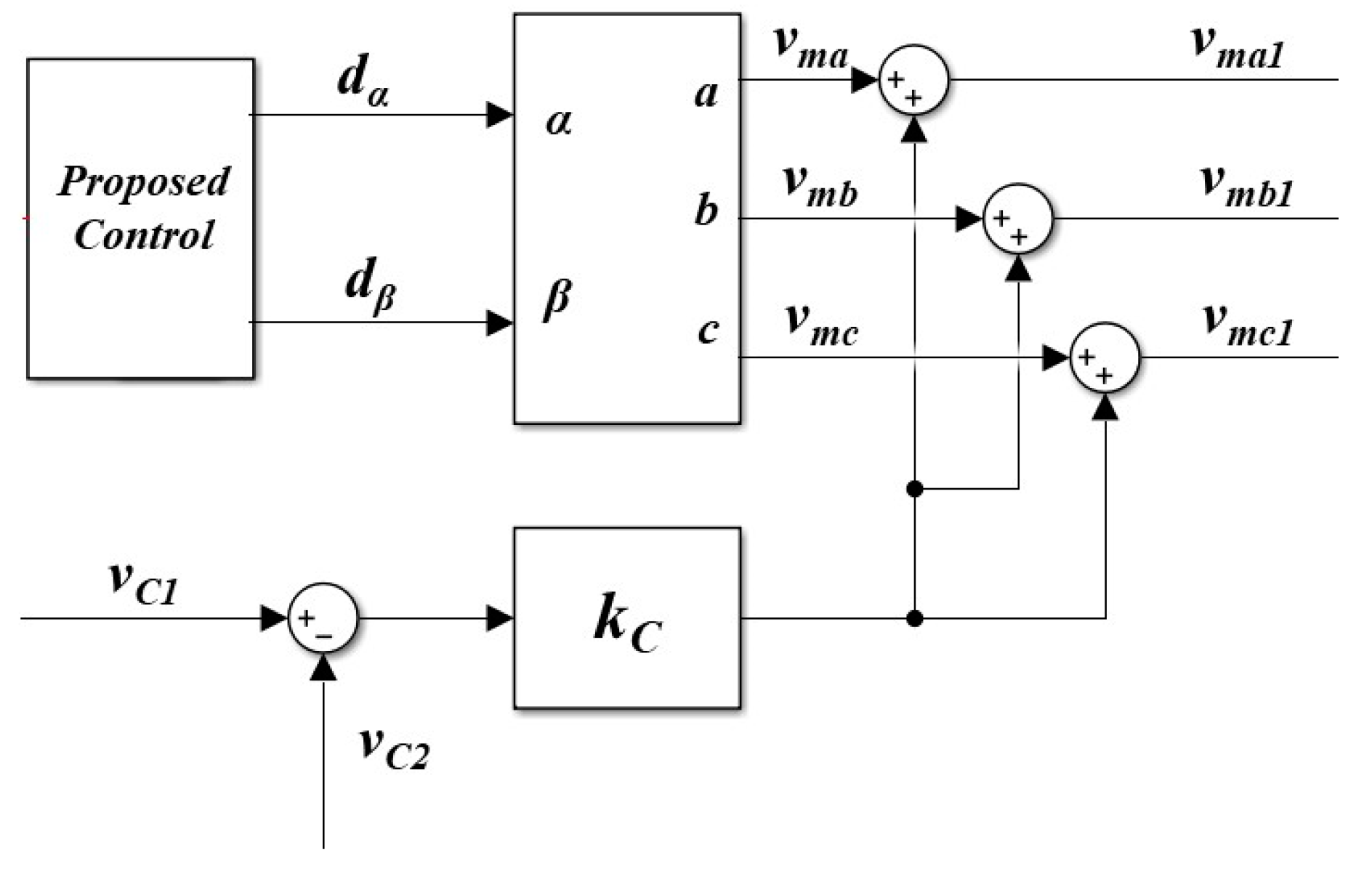
4.4. DC-Link Capacitors Voltage Balancing Control
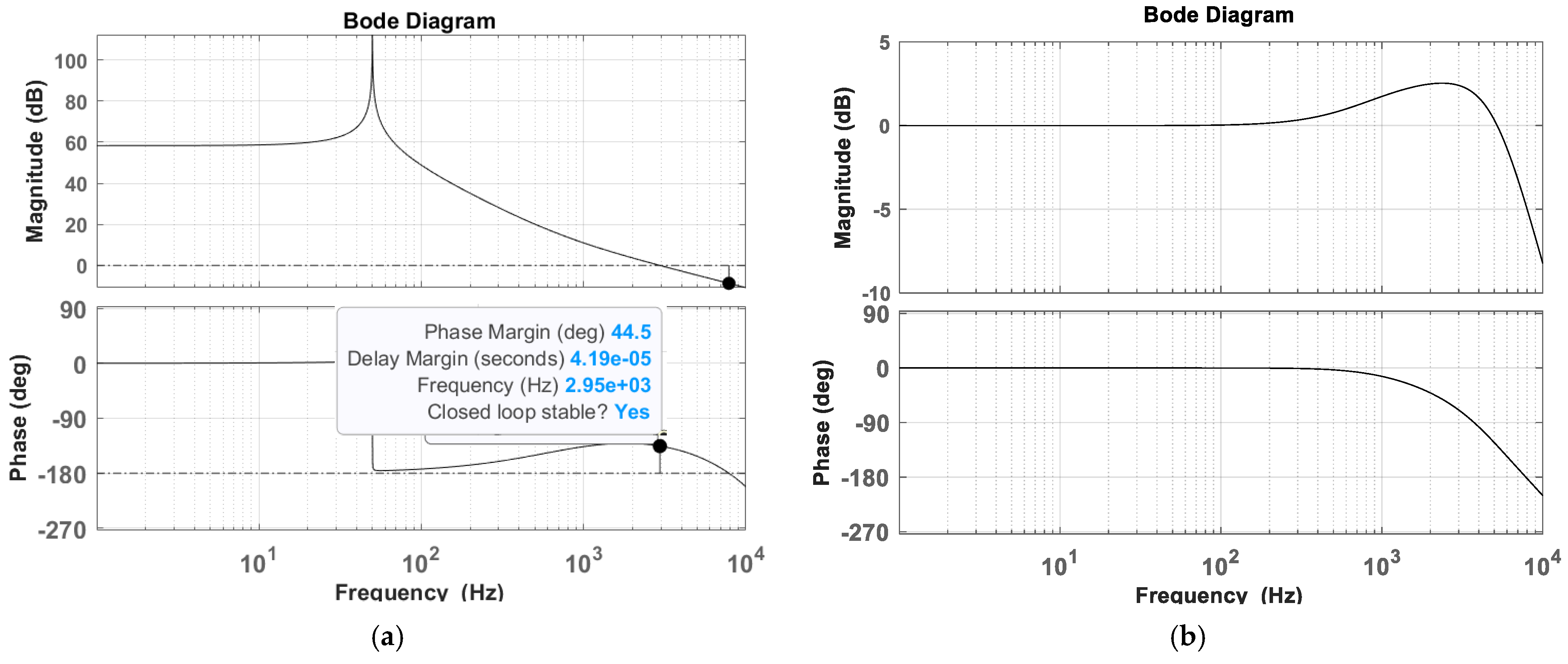
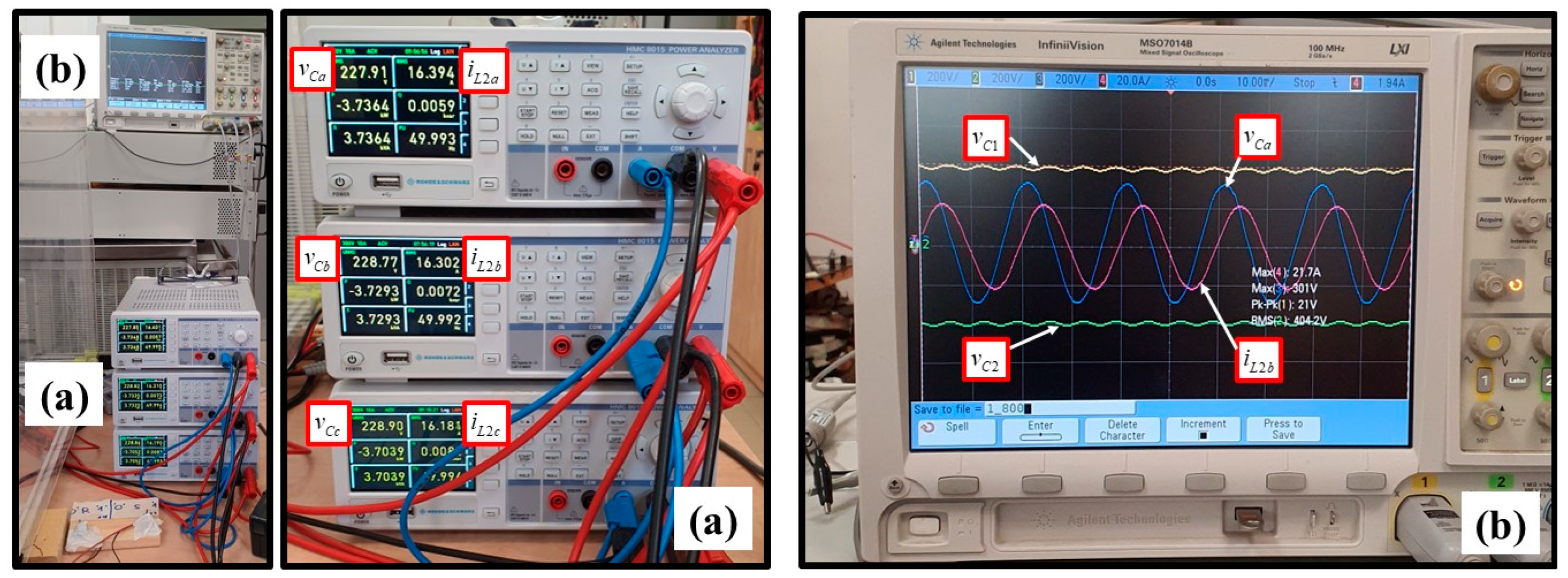
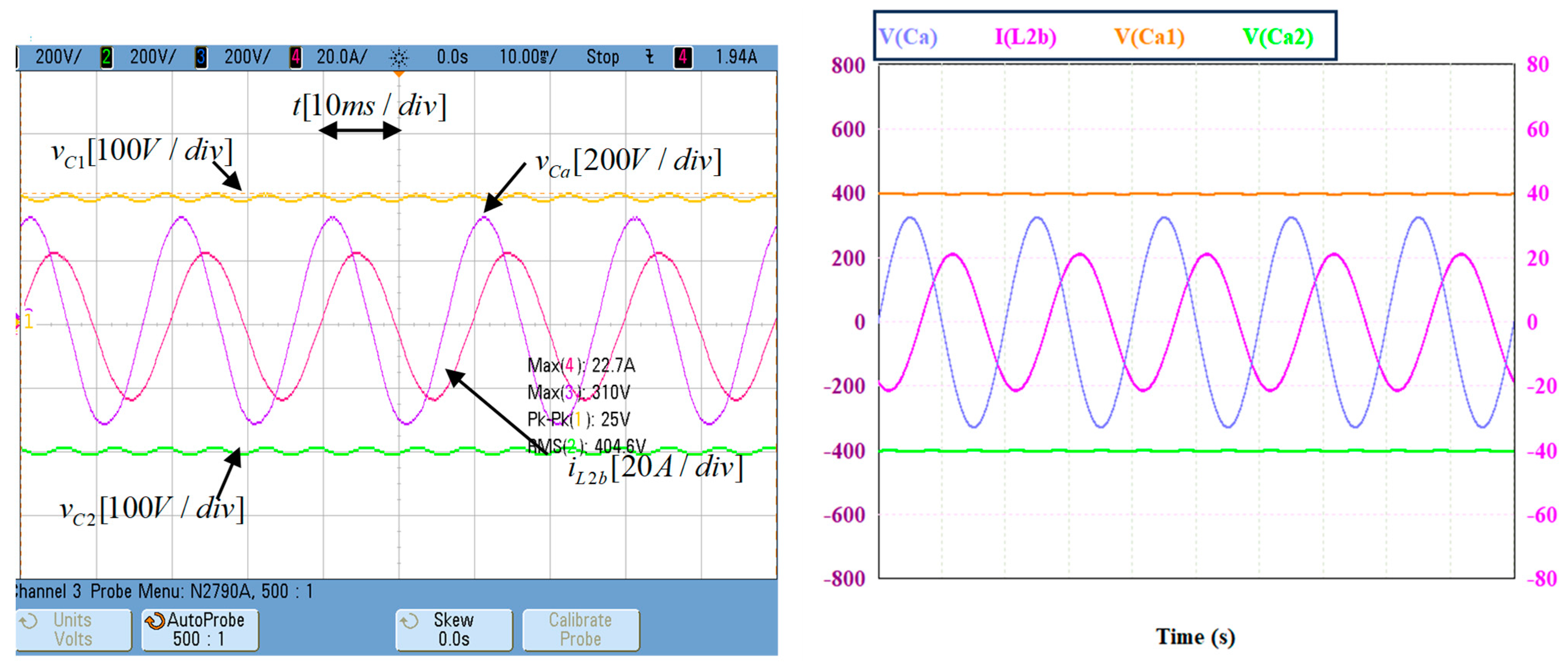
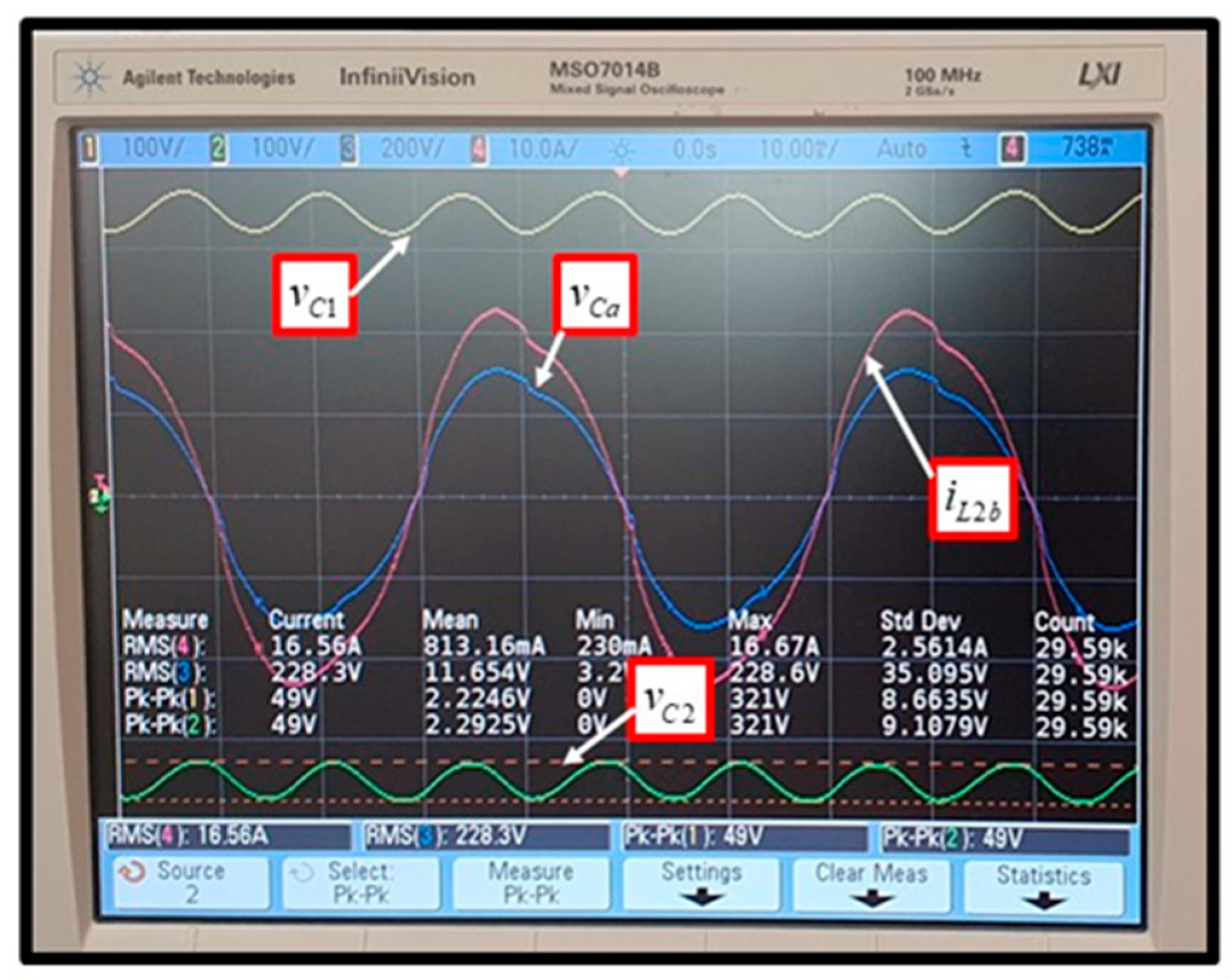
The voltage imbalance of the DC-link capacitors is the main technical challenge of the T-type topology. Imbalanced capacitor voltages can lead to reduced system performance, increased losses, and potential damage to the converter. Effective balancing control is proposed in this paper to ensure operational stability. As shown in Figure 4, vC1 is the voltage value across the DC link capacitor C1, and vC2 is the voltage value of capacitor C2. Figure 9 illustrates the proposed control strategy. The control algorithm is implemented in αβ stationary frame. The proposed control outputs dα and dβ (cf. Figure 6) transform from the αβ coordinate to the abc coordinate. The difference between capacitors voltages is multiplied by proportional controller, where kC is the proportional controller coefficient, and the controller output is added to the modulation signal vmx, where x refers to the phases a, b, and c, to achieve capacitor voltage balance by compensating for the neutral point current, as in the following:
v m a 1 = v m a + k C ( v C 1 v C 2 ) v m b 1 = v m b + k C ( v C 1 v C 2 ) v m c 1 = v m c + k C ( v C 1 v C 2 )
where vma, vmb, and vmc are the modulation signals of phases a, b, and c before the correction, and vma1, vmb1, and vmc1 are the modulation signals after the correction as shown in Figure 9. The proportional gain kC is selected to achieve a balance between response speed and system stability. A higher kC results in faster voltage correction but may introduce oscillations, while a lower kC provides a more stable response at the cost of slower balancing. Based on control stability analysis, the gain is tuned to prevent excessive overshoot and ensure smooth voltage regulation.

5. Verification

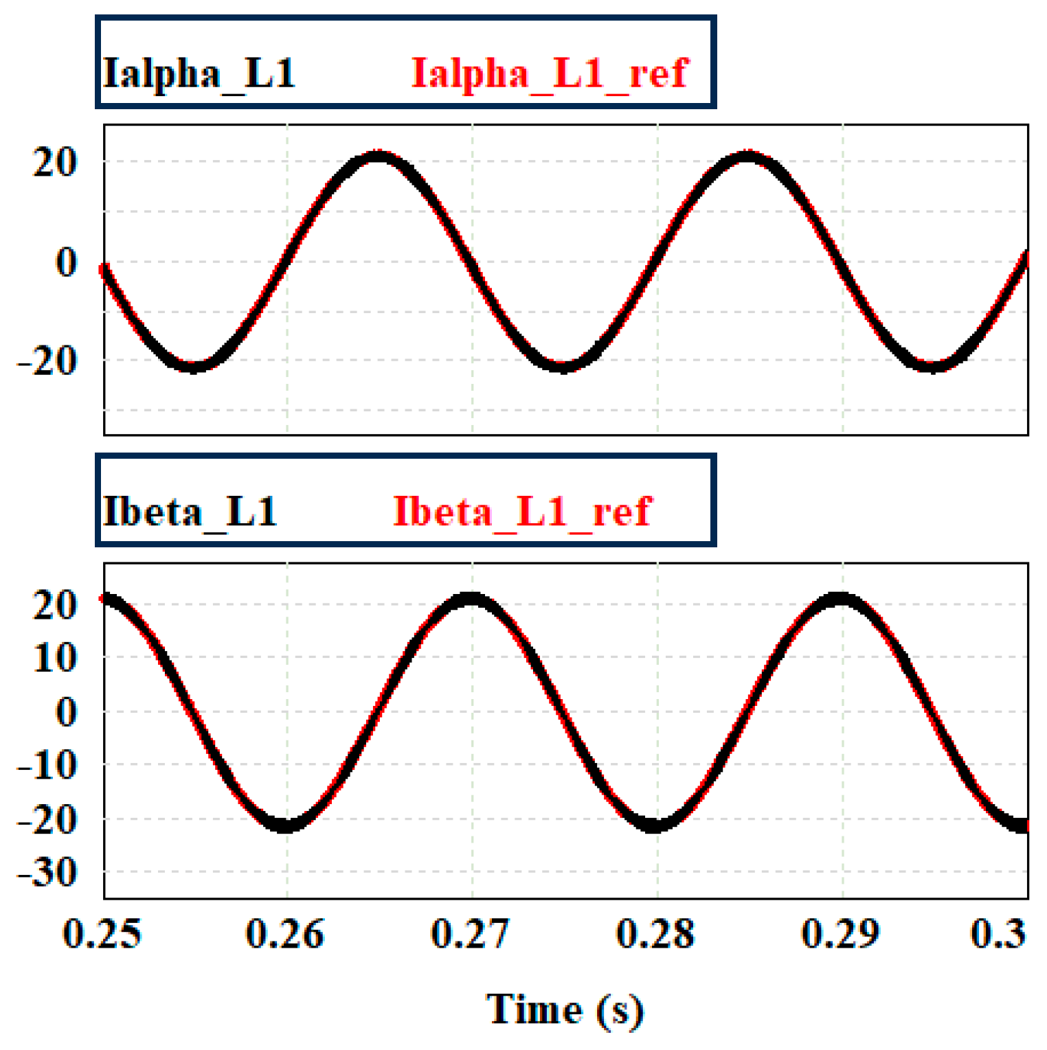
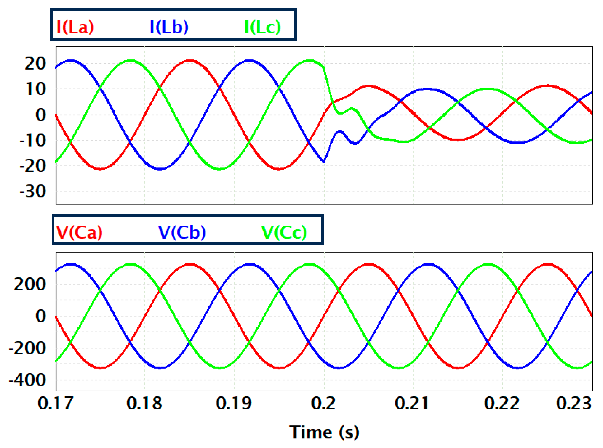
5.1. Simulation Validation

Simultaneously, simulations were performed using Powersim software to validate the feasibility of the proposed control. The proposed control was applied on a three-level, three-phase T-type inverter, as shown in Figure 4, with designed parameters listed in Table 1. Simulation results are shown in Figure 10, Figure 11, Figure 12 and Figure 13. Figure 10 and Figure 11 demonstrate the capability of the proposed design of precise tracking. The reference and output α and β control loops of the capacitor/output voltage outer loop (Figure 10) and the inverter side inductor current (Figure 11). Three phase signals of the output voltage (top) and inverter current (bottom) are shown in Figure 12. It may be concluded that tracking performance remains satisfactory at all times, demonstrating the validity and robustness of the proposed controller. Figure 13 demonstrates the DC-link capacitors’ voltage balancing control. Figure 13a shows zoomed-in results of the DC-link capacitors voltage vC1 and vC2. Results clearly show that voltage balancing loop control stabilizes the voltage difference between the DC-link capacitors. Figure 13b shows the modulation signals of the three phases before vmx (top) and after vmx1 (bottom), the correction of the three phases. Figure 14 illustrates the ability of the proposed design to accurately track sudden step changes in the reference signal magnitude, even under worst-case conditions caused by abrupt load variations. The simulation results further confirm that the system effectively maintains precise tracking of these step changes, achieving near-zero steady-state error. To conclude, the simulation results obtained have clearly proved the solid performance of the proposed controller.

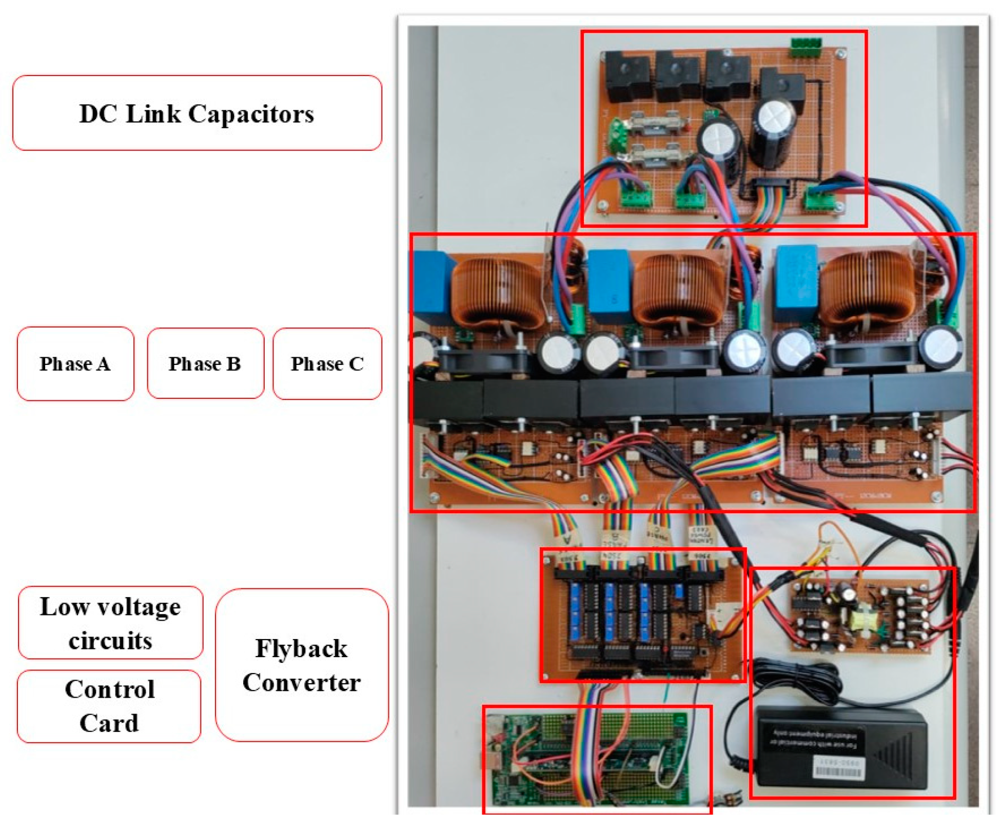
5.2. Experimental Results

The experimental setup for a three-level, three-phase T-type converter with an LCL filter prototype was designed and tested, as shown in Figure 15. It can be seen that the proposed control was implemented digitally using the Delfino F28335 control card. The resonant controllers that are employed in the proposed control algorithm are very sensitive to the discretization process due to their narrow band and infinite gain. A slight displacement of the resonant poles causes a significant loss of performance. At the first stage, the power source supplies DC 800 [V], which is split into two capacitors, each holding 400 [V]. These capacitors act as the DC link and serve as the power source for the T-type inverter. The proposed T-type inverter consists of two main switching blocks: Si-IGBT transistors and SiC-MOSFET transistors. In each phase, two Si-IGBT transistors function as a bidirectional switch, alternating the voltage polarity at the load with a 50 [Hz] frequency while operating at a switching frequency of 50 [KHz]. The SiC-MOSFET transistors are responsible for generating the PWM signal, ensuring that the output voltage maintains the same average value as a sine wave. This topology is based on a buck converter with a 50 [KHz] switching frequency, allowing efficient power conversion with reduced losses. The output voltage of the T-type inverter is connected to an LCL filter, which effectively attenuates high-frequency harmonics generated by the square wave switching process. To minimize power losses associated with transistor switching, SiC-MOSFET transistors were selected, as they enable higher switching frequencies, reducing the required size of the LCL filter inductors and capacitors, thereby optimizing system efficiency and compactness. Recent advancements in switching devices, such as GaN transistors, have further improved power electronics by offering even lower conduction and switching losses. However, in this system, SiC MOSFETs (Mouser Electronics, Mansfield, TX, USA) were chosen over GaN transistors due to their superior performance in high-power applications, better thermal management, and higher voltage handling capabilities, making them more suitable for the 800 [V] input voltage used in this setup. The discrete version of the proposed controllers (C1(s) and C2(s)) have been derived using first-order hold (FOH) transformation, which is the most accurate discretization method for resonant controllers. System parameters are the same as simulations and are given in Table 1. The converter was connected to a 10 kW power load. Figure 16a shows the actual experimental values of all three phases, including the RMS values of capacitor voltages and inverter currents and fundamental frequency. Figure 16b presents the time-domain signals of the DC-link capacitors voltages, confirming they are balanced as anticipated, along with the capacitor voltage of phase a and the current of phase b. In addition, Figure 17 compares results from the simulation (right) and experiment (left). Both the desired voltage levels and sinusoidal current are achieved with precision using the proposed dual-loop control and DC-link capacitor voltage balancing strategy, as demonstrated by identical results.
To further evaluate the performance of the proposed control strategy, a comparative analysis was conducted using conventional PI controllers instead of the resonant controllers. The experimental results are presented in Figure 18 and reveal that when PI controllers are applied, both gain and phase errors are introduced. Specifically, the measured results display the output voltage of phase a and the current of phase b, which ideally should have a 120° phase shift as shown in the proposed control results in Figure 17, yet an undesired 180° shift is observed as shown in Figure 18. Additionally, harmonic distortion is evident in both voltage and current waveforms, leading to signal distortion and reduced power quality. These results confirm that the PI-based approach exhibits steady-state errors, failing to maintain accurate tracking, whereas the proposed resonant-based controllers significantly improve system performance by ensuring precise phase alignment and reducing harmonic content.

6. Conclusions

This paper presents a dual-loop control system for three-level three-phase T-type converters in the hybrid operation of P2X systems. The proposed control strategy, incorporating both an inner current loop with a proportional-resonant controller and FF action to eliminate disturbances and an outer voltage loop with a proportional-resonant controller, has proven to be highly effective in managing the complexities and dynamics of P2X applications. In addition, a novel control strategy was added to the control loop to balance the DC side capacitors’ voltages and maintain system stability. The identified control loops are discussed in detail in this paper, and comprehensive simulation and experimental results demonstrate that this control approach ensures precise regulation of converter output, which enhances the efficiency, stability, and overall effectiveness of P2X systems hybrid operation.
Looking ahead, future research should explore the integration of machine learning-based controllers to enhance system adaptability and robustness, particularly in dynamic and uncertain grid conditions. Machine learning techniques can optimize controller parameters in real time, improving performance beyond traditional control methods. Additionally, hardware optimizations and other enhancement strategies should be investigated to improve system efficiency, reduce switching losses, and lower overall costs, with a focus on advanced semiconductor materials and optimized circuit topologies. Another important direction is the expansion of the proposed control strategy to smart grid applications, enabling seamless integration of P2X systems into future energy networks and addressing bidirectional energy flow, demand-side management, and grid interaction stability. Moreover, exploring advanced control techniques such as adaptive control, predictive control, and nonlinear control methods could further improve tracking accuracy, transient response, and overall system robustness. Finally, an important extension of this work is the development of a triple-loop control configuration incorporating FF action, which would build upon the current dual-loop approach to provide even greater disturbance rejection and enhanced control over system dynamics. By addressing these areas, future research can further optimize the proposed control system, enhance its efficiency, and ensure its successful deployment in large-scale, real-world P2X applications.

Author Contributions

Methodology, M.S.E.; Software, M.S.E.; Validation, M.S.E.; Investigation, M.S.E.; Writing—original draft, M.S.E.; Supervision, D.V. All authors have read and agreed to the published version of the manuscript.

Funding

This research was supported in part by the Estonian Research Council grant PRG1086 and in part by the Estonian Centre of Excellence in Energy Efficiency, ENER (grant TK230) funded by the Estonian Ministry of Education and Research.

Institutional Review Board Statement

Not applicable.

Informed Consent Statement

Not applicable.

Data Availability Statement

The original contributions presented in this study are included in the article. Further inquiries can be directed to the corresponding author.

Conflicts of Interest

The authors declare no conflict of interest.

References

  1. Zhao, G.; Liu, J.; Liu, S.; Zhou, X.; Li, J.; Lu, Y. Control Strategy Based on the Flexible Multi-State Switch for Maximum Consumption of Distributed Generations in Distribution Network. Appl. Sci. 2019, 9, 2871. [Google Scholar] [CrossRef]
  2. Rasool, M.; Khan, M.A.; Aurangzeb, K.; Alhussein, M.; Jamal, M.A. Comprehensive techno-economic analysis of a standalone renewable energy system for simultaneous electrical load management and hydrogen generation for fuel cell electric vehicles. Energy Rep. 2024, 11, 6255–6274. [Google Scholar] [CrossRef]
  3. Rausell, E.; Navarro, G.; Lafoz, M.; Arnaltes, S.; Rodríguez, J.L.; Blanco, M. Analysis of using MMC topologies for the direct integration of renewable generation with modular electrolyzers. In Proceedings of the 2023 25th European Conference on Power Electronics and Applications (EPE’23 ECCE Europe), Aalborg, Denmark, 4–8 September 2023. [Google Scholar]
  4. Chen, M.; Chou, S.-F.; Blaabjerg, F.; Davari, P. Overview of power electronic converter topologies enabling large-scale hydrogen production via water electrolysis. Appl. Sci. 2022, 12, 1906. [Google Scholar] [CrossRef]
  5. Xing, X.; Lin, J.; Song, Y.; Zhou, Y.; Mu, S.; Hu, Q. Modeling and operation of the power-to-gas system for renewables integration: A review. CSEE J. Power Energy Syst. 2018, 4, 168–178. [Google Scholar] [CrossRef]
  6. Nady, S.; El Fadil, H.; Koundi, M.; Hamed, A.; Giri, F. Power to X systems: State-of-the-art. IFAC-Pap. 2022, 55, 300–305. [Google Scholar] [CrossRef]
  7. Ghirardi, E.; Brumana, G.; Franchini, G.; Aristolao, N.; Vedovati, G. The role of hydrogen storage and electric vehicles in grid-isolated hybrid energy system with high penetration of renewable. Energy Convers. Manag. 2024, 302, 118154. [Google Scholar] [CrossRef]
  8. Bibiloni, S.; Irimescu, A.; Martinez-Boggio, S.; Merola, S.; Curto-Risso, P. Mild Hybrid Powertrain for Mitigating Loss of Volumetric Efficiency and Improving Fuel Economy of Gasoline Vehicles Converted to Hydrogen Fueling. Machines 2024, 12, 355. [Google Scholar] [CrossRef]
  9. Ruuskanen, V.; Koponen, J.; Kosonen, A.; Hehemann, M.; Keller, R.; Niemelä, M.; Ahola, J. Power quality estimation of water electrolyzers based on current and voltage measurements. J. Power Sources 2020, 450, 227603. [Google Scholar] [CrossRef]
  10. Vule, Y.; Siton, Y.; Kuperman, A. Comprehensive modeling and formulation of split DC link capacitors balancing problem in three-phase three-level bidirectional AC/DC converters operating with arbitrary power factor. Alex. Eng. J. 2023, 83, 195–211. [Google Scholar] [CrossRef]
  11. Chen, Z.; Zheng, T.; Liu, C. An Islanding Signal-Based Smooth Transition Control in AC/DC Hybrid Micro-Grids. Appl. Sci. 2019, 9, 2804. [Google Scholar] [CrossRef]
  12. Schweizer, M.; Kolar, J.W. Design and implementation of a highly efficient threelevel T-type converter for low-voltage applications. IEEE Trans. Power Electron. 2013, 28, 899–907. [Google Scholar] [CrossRef]
  13. Floricau, D.; Floricau, E.; Gateau, G. Three-level active NPC converter: PWM strategies and loss distribution. In Proceedings of the 2008 34th Annual Conference of IEEE Industrial Electronics (IEEE IEAC), Orlando, FL, USA, 10–13 November 2008; pp. 3333–3338. [Google Scholar]
  14. Nabae, A.; Takahashi, I.; Akagi, H. A new neutral-point-clamped PWM inverter. IEEE Trans. Ind. Appl. 1981, IA-17, 518–523. [Google Scholar] [CrossRef]
  15. Harbi, I.; Rodriguez, J.; Poorfakhraei, A.; Vahedi, H.; Guse, M.; Trabelsi, M.; Abdelrahem, M.; Ahmed, M.; Fahad, M.; Lin, C.-H.; et al. Common DC-Link Multilevel Converters: Topologies, Control and Industrial Applications. IEEE Open J. Power Electron. 2023, 4, 512–538. [Google Scholar] [CrossRef]
  16. Baimel, D.; Barbie, E.; Bronshtein, S.; Sitbon, M.; Aharon, I.; Kuperman, A. High power T-type-based multi-level inverter for electric vehicles. Energy Rep. 2023, 9 (Suppl. S12), 220–225. [Google Scholar] [CrossRef]
  17. Boulmrharj, S.; Khaidar, M.; Bakhouya, M.; Ouladsine, R.; Siniti, M.; Zine-Dine, K. Performance assessment of a hybrid system with hydrogen storage and fuel cell for cogeneration in buildings. Sustainability. Sustainability 2020, 12, 4832. [Google Scholar] [CrossRef]
  18. Elkayam, M.; Kuperman, A. Optimized design of multiresonant AC current regulators for single-phase grid-connected photovoltaic inverters. IEEE J. Photovolt. 2019, 9, 1815–1818. [Google Scholar] [CrossRef]
  19. Sitbon, M.; Schacham, S.; Kuperman, A. Disturbance Observer-Based Voltage Regulation of Current-Mode-Boost-Converter-Interfaced Photovoltaic Generator. IEEE Trans. Ind. Electron. 2015, 62, 5776–5785. [Google Scholar] [CrossRef]
  20. Busada, C.A.; Jorge, S.G.; Leon, A.E.; Solsona, J.A. Current controller based on reduced order generalized integrators for distributed generation systems. IEEE Trans. Ind. Electron. 2012, 59, 2898–2909. [Google Scholar] [CrossRef]
  21. Wang, J.; Wei, H.; Dou, S.; Gillbanks, J.; Zhao, X. Active Disturbance Rejection Control Based on an Improved Topology Strategy and Padé Approximation in LCL-Filtered Photovoltaic Grid-Connected Inverters. Appl. Sci. 2024, 14, 11133. [Google Scholar] [CrossRef]
  22. Blaabjerg; Teodorescu, R.; Liserre, M.; Timbus, A. Overview of control and grid synchronization for distributed power generation systems. IEEE Trans. Ind. Electron. 2006, 53, 1398–1409. [Google Scholar] [CrossRef]
  23. Martínez-Turégano, J.; Sala, A.; Blasco-Gimenez, R.; Blanes, C. Operation of DR–HVdc-Connected Grid-Forming Wind Turbine Converters Using Robust Loop-Shaping Controllers. Appl. Sci. 2024, 14, 881. [Google Scholar] [CrossRef]
  24. Kuperman, A. Synchronous frame current controllers design based on desired stationary frame transient performance. Electron. Lett. 2015, 51, 1769–1770. [Google Scholar] [CrossRef]
  25. Sato, Y.; Ishizuka, T.; Nezu, K.; Kataoka, T. A new control strategy for voltage-type PWM rectifiers to realize zero steady-state control error to input current. IEEE Trans. Ind. Appl. 1998, 34, 480–486. [Google Scholar] [CrossRef]
  26. Zmood, D.; Holmes, D.; Bode, G. Frequency domain analysis of three-phase linear current regulators. IEEE Trans. Ind. Appl. 2001, 37, 601–610. [Google Scholar] [CrossRef]
  27. Zmood, D.; Holmes, G. Stationary frame current regulation of PWM inverters with zero steady-state error. IEEE Trans. Power Electron. 2003, 18, 814–822. [Google Scholar] [CrossRef]
  28. He, R.; Xue, B.; Zhou, M.; Fu, M.; Liang, J.; Liu, Y.; Wang, H. Resonant Frequency Tracking Scheme for LLC Converter Based on Large and Small Signal Combined Model. IEEE Access 2023, 11, 83390–83399. [Google Scholar] [CrossRef]
  29. Holmes, D.; Lipo, T.; McGrath, B.; Kong, W. Optimized design of stationary frame three phase AC current regulators. IEEE Trans. Power Electron. 2009, 24, 2417–2426. [Google Scholar] [CrossRef]
  30. Chiang, L.; Newman, M.; Zmood, D.; Holmes, D. A comparative analysis of multiloop voltage regulation strategies for single and three-phase UPS systems. IEEE Trans. Power Electron. 2005, 18, 1176–1185. [Google Scholar]
  31. Wei, Z.; Lu, D.; Agelidis, V. Current control of grid-connected boost inverter with zero steady-state error. IEEE Trans. Power Electron. 2011, 26, 2825–2834. [Google Scholar]
  32. Dong, D.; Thacker, T.; Fei, R.B.W.; Boroyevich, D. On zero steady-state error voltage control of single-phase PWM inverters with different load types. IEEE Trans. Power Electron. 2011, 26, 3285–3297. [Google Scholar] [CrossRef]
  33. Akagi, H.; Watanabe, E.H.; Aredes, M. Instantaneous Power Theory and Applications to Power Conditioning; El-Hawari, M.E., Ed.; Wiley-IEEE Press: Hoboken, NJ, USA, 2007. [Google Scholar]
  34. Xiaoguang, Z.; Qingyao, H. Digital Feed-Forward Control Based on Motor Closed-Loop System Identification. In Proceedings of the 2010 Second International Conference on Computer Modeling and Simulation, Sanya, China, 22–24 January 2010. [Google Scholar]
  35. Kuperman, A. Proportional-resonant current controllers design based on desired transient performance. IEEE Trans. Power Electron. 2015, 30, 5341–5345. [Google Scholar] [CrossRef]
  36. Elkayam, M.; Kolesnik, S.; Basha, Y.; Kuperman, A. Loop shaping by single-resonant controllers for prescribed tracking of sinusoidal references. IEEE Trans. Power Electron. 2019, 34, 11352–11360. [Google Scholar] [CrossRef]
  37. Akagi, H.; Hatada, T. Voltage balancing control for a three-level diode-clamped converter in a medium-voltage transformer less hybrid active filter. IEEE Trans. Power Electron. 2009, 24, 571–579. [Google Scholar] [CrossRef]
  38. Umbría, F.; Gordillo, F.; Gómez-Estern, F.; Salas, F.; Portillo, R.C.; Vázquez, S. Voltage balancing in three-level neutral-point-clamped converters via Luenberger observer. Control Eng. Pract. 2014, 25, 36–44. [Google Scholar] [CrossRef]
  39. Gadelovits, S.; Kadirkamanathan, Q.-C.Z.V.; Kuperman, A. UDE-based controller equipped with a multi-band-stop filter to improve the voltage quality of inverters. IEEE Trans. Ind. Electron. 2017, 64, 7433–7443. [Google Scholar] [CrossRef]
Figure 1. Block diagram of the proposed hybrid system.
Applsci 15 02409 g001
Figure 2. Bidirectional three-level three-phase T-type converter.
Applsci 15 02409 g002
Figure 3. T-type converter employed in the hybrid system.
Applsci 15 02409 g003
Figure 4. Three-level three-phase T-type converter with the LCL filter.
Applsci 15 02409 g004
Figure 5. Single-phase LCL-filter-based converter representation.
Applsci 15 02409 g005
Figure 6. Block diagram of the proposed control structure.
Applsci 15 02409 g006
Figure 7. (a) Open-loop and (b) closed-loop Bode diagrams of the current loop.
Applsci 15 02409 g007
Figure 9. Block diagram of the DC-link capacitors voltage balancing control.
Applsci 15 02409 g009
Figure 10. Simulation results of the capacitor voltage reference and output signals of both α (top) and β (bottom) loops.
Applsci 15 02409 g010
Figure 11. Simulation results of the inverter side inductor current reference and output signals of both α (top) and β (bottom) loops.
Applsci 15 02409 g011
Figure 12. Simulation results of the three-phase signals of output voltages (top) and inverter side inductors currents (bottom).
Applsci 15 02409 g012
Figure 13. Simulation results of (a) DC-link capacitors voltages and (b) modulation signals of the three phases before (top) and after (bottom) the correction.
Applsci 15 02409 g013
Figure 14. Simulation results three phase signals of output voltages and inverter side inductors currents.
Applsci 15 02409 g014
Figure 15. A three-level, three-phase T-type LCL filtered converter experimental platform.
Applsci 15 02409 g015
Figure 16. (a) Experiment values of the three phases and (b) experimental results of the DC-link capacitors voltages (top and bottom), the capacitor voltage of phase a, and the inverter current of phase b (The displayed frequency is 49.99 in all phases).
Applsci 15 02409 g016
Figure 17. Comparison between experimental results (left) and simulation (right), including DC side capacitors voltages, the output voltage across the filter capacitor of phase a, and the current of phase b.
Applsci 15 02409 g017
Figure 18. Comparison between experimental results of DC-link capacitors voltages (top and bottom), capacitor voltage of phase a, and inverter current of phase b with PI controller.
Applsci 15 02409 g018
Table 1. System Parameters.
ParameterValueUnits
Switching and sampling frequency, Ts−150 kHz
Filter inductors, L1x340μH
AC side inductors, L2x9.43μH
Filter capacitors, Cx10μF
DC link capacitors, C1, C2460μF
Fundamental frequency, f050Hz
Fundamental frequency, ω0100πrad/s
DC voltage, VDC800V
Damping factor, ζ0.001
Proportional gain, kC0.06
Disclaimer/Publisher’s Note: The statements, opinions and data contained in all publications are solely those of the individual author(s) and contributor(s) and not of MDPI and/or the editor(s). MDPI and/or the editor(s) disclaim responsibility for any injury to people or property resulting from any ideas, methods, instructions or products referred to in the content.

