Article

A Design Methodology for Low-Loss Interconnects Featuring Air Cavities and Periodically Nonuniform Widths

College of Information, Mechanical and Electrical Engineering, Shanghai Normal University, 100-GuilinRoad, Shanghai 200234, China
*
Author to whom correspondence should be addressed.
Appl. Sci. 2025, 15(5), 2799; https://doi.org/10.3390/app15052799
Submission received: 16 January 2025 / Revised: 24 February 2025 / Accepted: 27 February 2025 / Published: 5 March 2025
(This article belongs to the Section Electrical, Electronics and Communications Engineering)

Abstract

:

Featured Application

This work demonstrates significant potential for applications in integrated circuits, attributed to its low loss and reduced power consumption.

Abstract

Power consumption in interconnects is a critical constraint on performance improvements in integrated circuits. This paper proposes a novel design methodology to minimize loss in interconnects and address this limitation. The approach incorporates air cavities within the substrate to lower the equivalent loss tangent, thereby reducing dielectric losses. Additionally, the inner conductor is engineered with a periodically nonuniform width to maintain stable effective characteristic impedance. To validate the effectiveness of the methodology, it is applied to both a substrate integrated coaxial line (SICL) and a stripline. Simulation results reveal a 9.76% reduction in loss for the SICL and a 19.40% reduction in loss for the stripline, demonstrating significant improvements with wide tolerance. Furthermore, this design methodology can be generalized to other interconnect types, offering the potential for additional power savings.

1. Introduction

With the rapid advancement of integrated circuit technology and manufacturing processes, circuit performance has significantly improved, benefiting a wide range of industries [1]. However, as feature sizes shrink and operating frequencies rise, issues like high power consumption and overheating have become more pronounced [2,3,4,5]. To tackle these challenges, the demand for low-loss circuit components has grown [6]. Given the increasing impact of interconnects in high-speed integrated circuits, researchers have been actively exploring solutions in the area of creating low-loss interconnects [7,8,9,10].
Interconnect losses mainly consist of radiation loss, conductor loss, and dielectric loss. To minimize radiation loss, quasi-shielded interconnects are preferred over open-structured types like microstriplines and striplines. Substrate-integrated waveguide (SIW) and substrate integrated coaxial line (SICL) are two common examples of such quasi-shielded interconnects with effective anti-crosstalk performance [11,12,13,14,15,16,17]. Conductor loss is reduced by suppressing the skin effect through the use of laminated lines, which provide a bandwidth ranging from DC to 40 GHz [18]. Dielectric loss is mitigated using an empty SICL, offering a bandwidth ranging from DC to 20 GHz [19]. A similar air-filled technology has been applied to an SIW and a better than 20 dB return loss was measured with a total back-to-back insertion loss of 0.5 ± 0.2 dB from the 57 to the 66 GHz band [20]. Using laminate dielectrics on a glass substrate, air-filled SIWs have been fabricated, demonstrating a measured per-unit insertion loss of 0.13 dB/mm in the D-band (110 to 170 GHz) [21]. A hollow rectangular dielectric waveguide, composed of three dielectric layers with a hollow structure created by cutting an air-filled slot in the middle layer, exhibits an average attenuation constant of 0.028 dB/mm across the 220–294 GHz frequency range, as supported by measurement results [22]. For integrated circuits, a self-aligned air-gap interconnect process is proposed in [23]. A misalignment-free multilevel air-gap interconnect with a via–base structure is fabricated using self-aligned gap formation and etch-back processes [24]. Air-gap transmission lines can also be fabricated on organic substrates for low-loss interconnects [25]. The modeling, optimization, and benchmarking of air-gap interconnects are discussed in [26]. Furthermore, periodically introducing air cavities can also reduce dielectric loss due to the low loss tangent of air. However, this approach may introduce discontinuities and impedance mismatches, leading to increased return losses and signal attenuation.
This work proposes a design methodology for low-loss interconnects featuring air cavities and periodically nonuniform conductor widths. In this approach, the columnar air cavities are utilized to reduce dielectric losses, while the nonuniform-width conductor is designed to compensate for impedance mismatches introduced by the cavities. To validate the effectiveness of the proposed methodology, it is applied to both an SICL and a stripline. Simulation results demonstrate that the SICL and stripline incorporating the proposed design exhibit reduced losses and improved impedance matching compared to conventional designs.

2. Materials and Methods

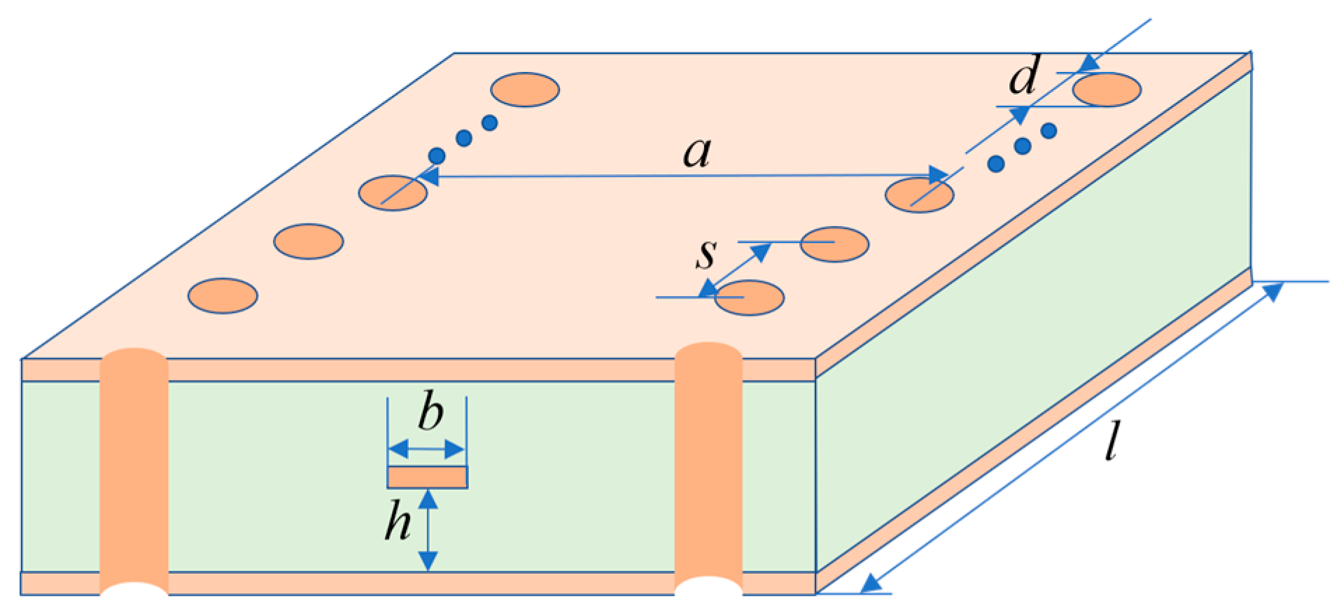
2.1. Challenges in the Current State of the Art

A two-conductor transmission line facilitated the propagation of transverse electromagnetic (TEM) waves [27]. Typically, such a transmission line consists of a thin signal line, a ground plane or two ground planes, and a dielectric material between them [28]. Introducing air cavities into the substrate is widely recognized as an effective strategy to reduce the loss tangent and, consequently, dielectric losses [19,20,21,22,23,24,25,26,29].
The use of large cavities spanning almost the entire dielectric substrate introduces additional challenges for integration processes and mechanical stress, whereas periodic small cavities are more conducive to integration. However, periodic small cavities can lead to impedance mismatches in the two-conductor transmission line. This challenge is analyzed in detail in the subsequent sections, and a methodology to mitigate it is proposed. To demonstrate the problem and its resolution, an SICL is utilized as a representative example. The SICL consists of an inner conductor, an outer conductor, and a dielectric material that separates them, as illustrated in Figure 1. The inner conductor is a metallic line, while the outer conductor is constructed from two metallic layers and two rows of metallic vias.
In Figure 1, l represents the length of the SICL, h is half the thickness of the dielectric layer, s is the spacing between adjacent vias, d is the diameter of the vias, and a and b are the widths of the outer and inner conductors, respectively. The TEM single-mode operating frequency band of the SICL ranges from DC to fTE10, which can be calculated using Equation (1) [11]:
f T E 10 = c 2 ε r a d 2 0.95 s 1
where c is the speed of light in a vacuum, and εr is the relative permittivity of the dielectric material.
Inserting air cavities into the substrate, within the constraints of allowable process limits, effectively reduces the equivalent loss tangent and, consequently, the dielectric loss. These air cavities can take various forms, such as rectangular prisms or cylinders. Figure 2 illustrates an SICL with two rows of periodically arranged cylindrical air cavities, where Y0 represents the longitudinal section through the middle of the substrate. To maintain sufficient mechanical strength in the substrate, the air cavities are spaced appropriately, as shown in the longitudinal section Y0 depicted in Figure 3a. The diameter of each air cavity is denoted as dₐ, the spacing between adjacent cavities as sₐ, and the distance between the two rows as wₐ.
However, the introduction of air cavities can result in mismatches of the effective characteristic impedance. The effective characteristic impedance of the transmission line with periodic air cavities at any cross-section can be defined as the characteristic impedance of a uniform transmission line formed by extending that cross-section along the direction of current propagation. As illustrated in Figure 3b, at cross-sections X1, X2, and X3 the ratio of air to the dielectric substrate varies. This variation leads to different effective relative permittivity values, such that εᵣ(X1) > εᵣ(X2) > εᵣ(X3). Consequently, the effective characteristic impedance at these positions follows the relationship Z(X1) < Z(X2) < Z(X3).

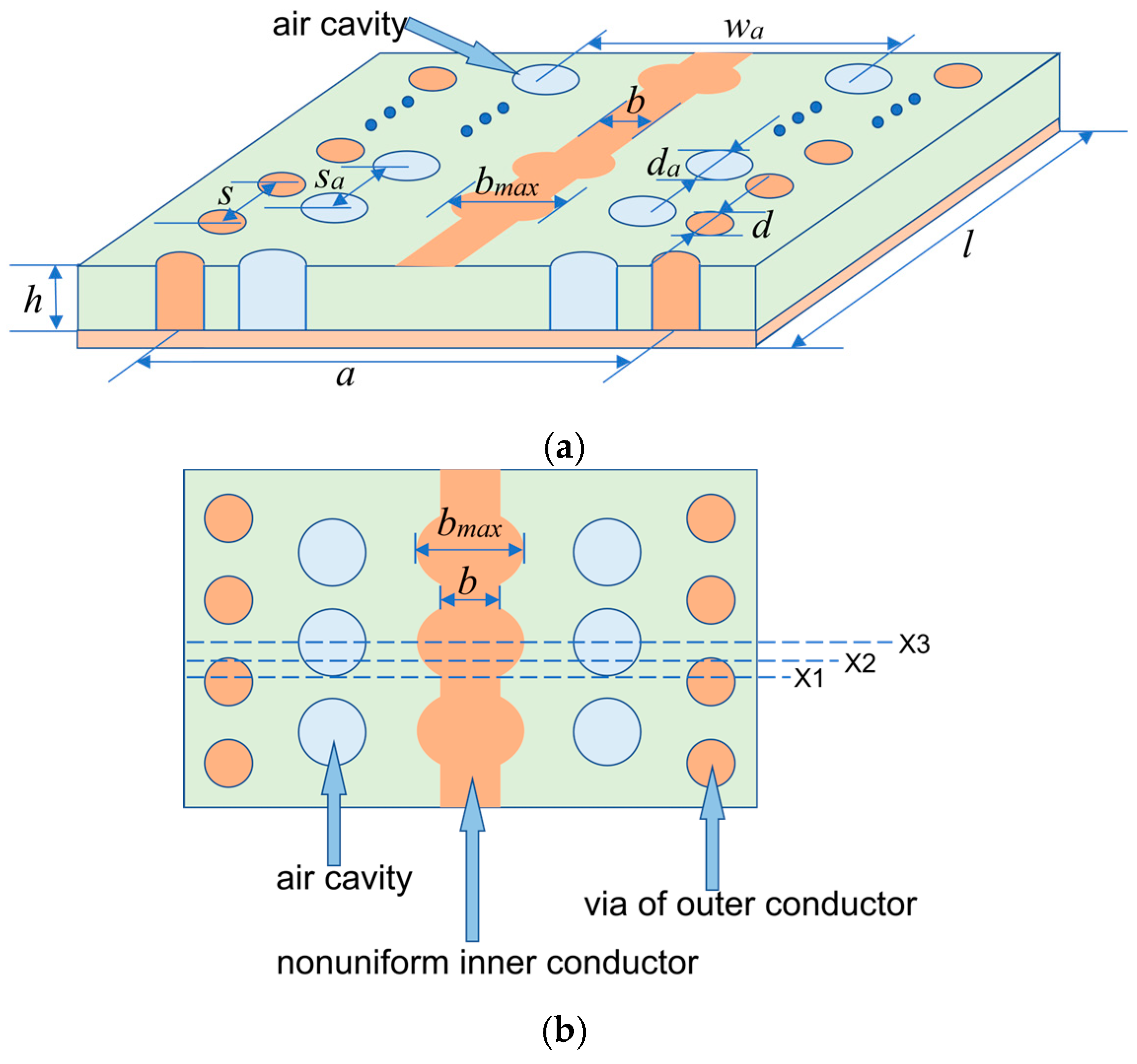
2.2. Transmission Structure Addressing the Current Challenge

To compensate for the effective characteristic impedance mismatches, an interconnect featuring a nonuniform-width inner conductor is proposed, as illustrated in Figure 4. The nonuniform-width inner conductor incorporates a periodic structure that aligns with the periodic cylindrical air cavities. The widest sections of the inner conductor occur at cross-sections where the air cavities are most pronounced, such as at X3, with the maximum width denoted as bₘₐₓ. The narrowest sections, located where no cavities are present, such as at X1, match the width of a traditional SICL, denoted as b. The inner conductor width is adjusted to maintain an effective characteristic impedance of 50 Ω at each cross-section, following the steps outlined below:
Step 1: Determine the width b of the inner conductor at cross-section X1, ensuring an effective characteristic impedance of 50 Ω.
Step 2: Calculate the maximum width bₘₐₓ of the inner conductor at cross-section x3, targeting an effective characteristic impedance of 50 Ω.
Step 3: Calculate the corresponding inner conductor widths for intermediate cross-sections between X1 and X3, maintaining an effective characteristic impedance of 50 Ω.
Step 4: Connect the calculated widths smoothly using a continuous curve to form a nonuniform-width unit.
Step 5: Periodically repeat the nonuniform width unit along the length of the interconnect.

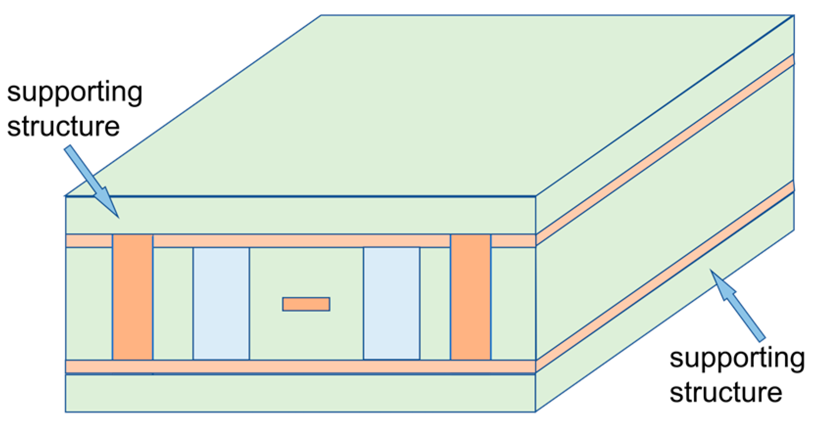
2.3. Supporting Structure

Although the aforementioned structure enables low-loss transmission, the ground plane is not continuous due to the presence of air cavities. To address this issue, two additional dielectric substrates are incorporated on the outer sides of the metallic layers, serving as a supporting structure. Intact metallic layers can then be printed on these substrates, as illustrated in Figure 5.

2.4. Demonstration Setup and Parameters

The proposed design methodology is applicable to common two-conductor transmission lines made from various materials and can be implemented using standard fabrication processes.
It should be noted that if the transmission line is used in power applications, or if the inner conductor carries a large DC current as part of the bias path for active devices, non-uniform dimensions may lead to reliability issues in the circuit. Therefore, if the methodology proposed in this paper is applied to such scenarios, the associated risks must be carefully evaluated.
To validate the effectiveness of the methodology, it is applied to both an SICL and a stripline. The low-temperature co-fired ceramic (LTCC) process is highly suitable for multilayer, high-density integrated circuits, is well-suited for high-frequency applications, and is capable of realizing cavity structures. These advantages align well with the requirements of this design methodology. In addition, LTCC Ferro A6M (Ferro, Cleveland, OH, USA) was selected as the dielectric substrate due to its stable relative permittivity with minimal variation across the 1–100 GHz frequency range [17,30]. For the simulations, an average relative permittivity of εᵣ = 5.8 and a loss tangent of 0.0012 are assumed. Copper is utilized as the conductor material.
For demonstration purposes, simulations are performed using a finite element method (FEM) solver, with the implementation based on the parameters outlined in Table 1.

3. Results

The simulation results for the SICL and stripline incorporating the proposed design methodology are presented in the following figures. For comparison, the results for their traditional counterparts are also included.

3.1. SICL Incorporating the Proposed Design Methodology

3.1.1. Loss Reduction

Interconnect loss can be assessed using the attenuation constant. As illustrated in Figure 6, the introduction of air cavities and a nonuniform-width inner conductor yields a 9.76% reduction in the attenuation constant at 100 GHz compared to the traditional SICL, attributed to the lower equivalent loss tangent. Additionally, when compared to the SICL with air cavities, the proposed design demonstrates a 5.76% decrease in the attenuation constant, primarily due to improvements in impedance matching. Notably, this improvement becomes more pronounced as the frequency increases.

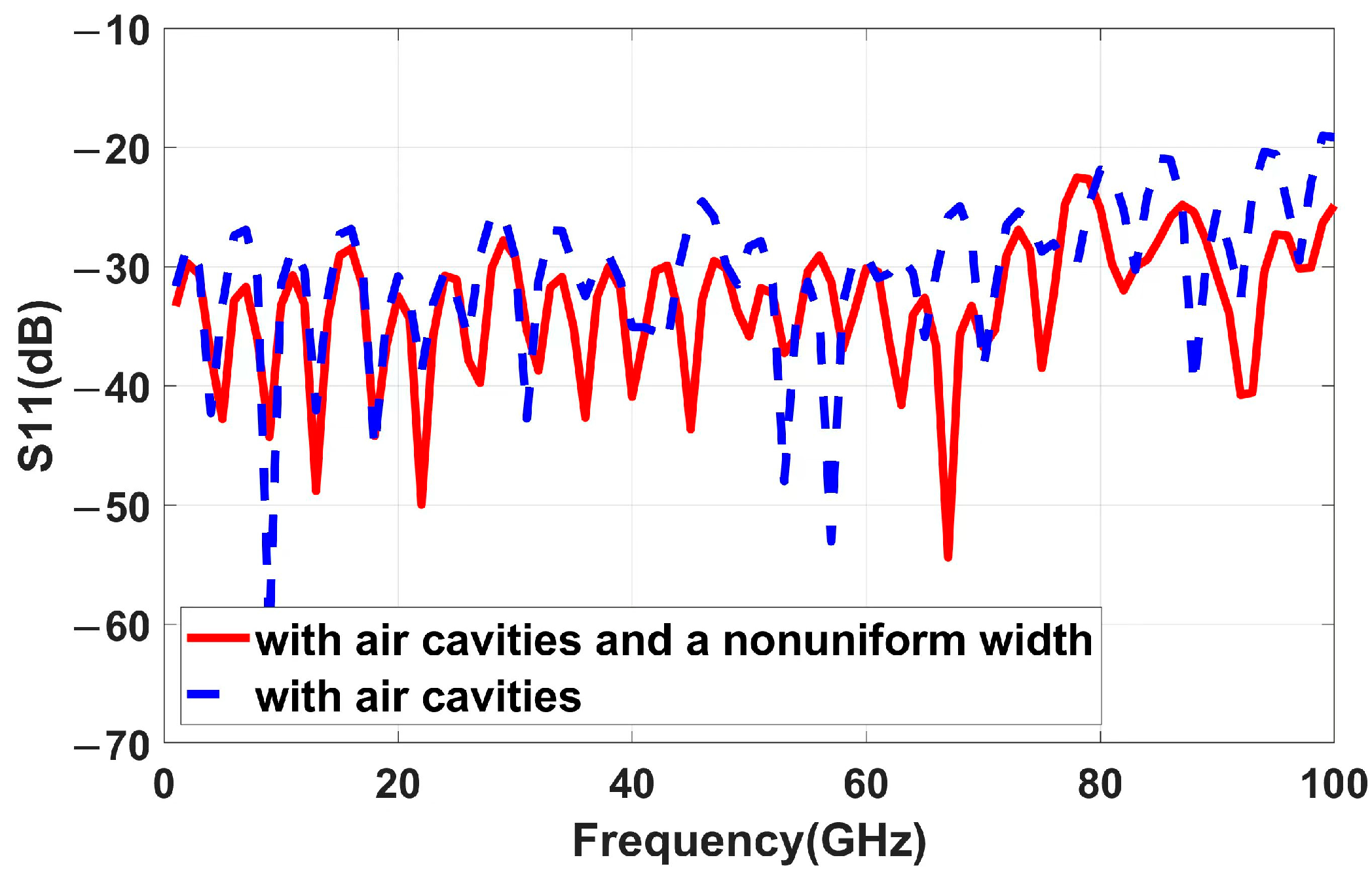
3.1.2. Improvement in Impedance Matching

The improvement in impedance matching is evident from the reduction in return loss. To evaluate the impact of the nonuniform-width inner conductor, the S11 parameters of two interconnects—both incorporating air cavities—are compared: one featuring the nonuniform-width inner conductor and the other a uniform-width conductor. As illustrated in Figure 7, the proposed interconnect achieves a reduction in S11 of approximately 5 dB compared to the configuration with air cavities alone, underscoring the effectiveness of the design methodology in enhancing impedance matching.

3.2. Stripline Incorporating the Proposed Design Methodology

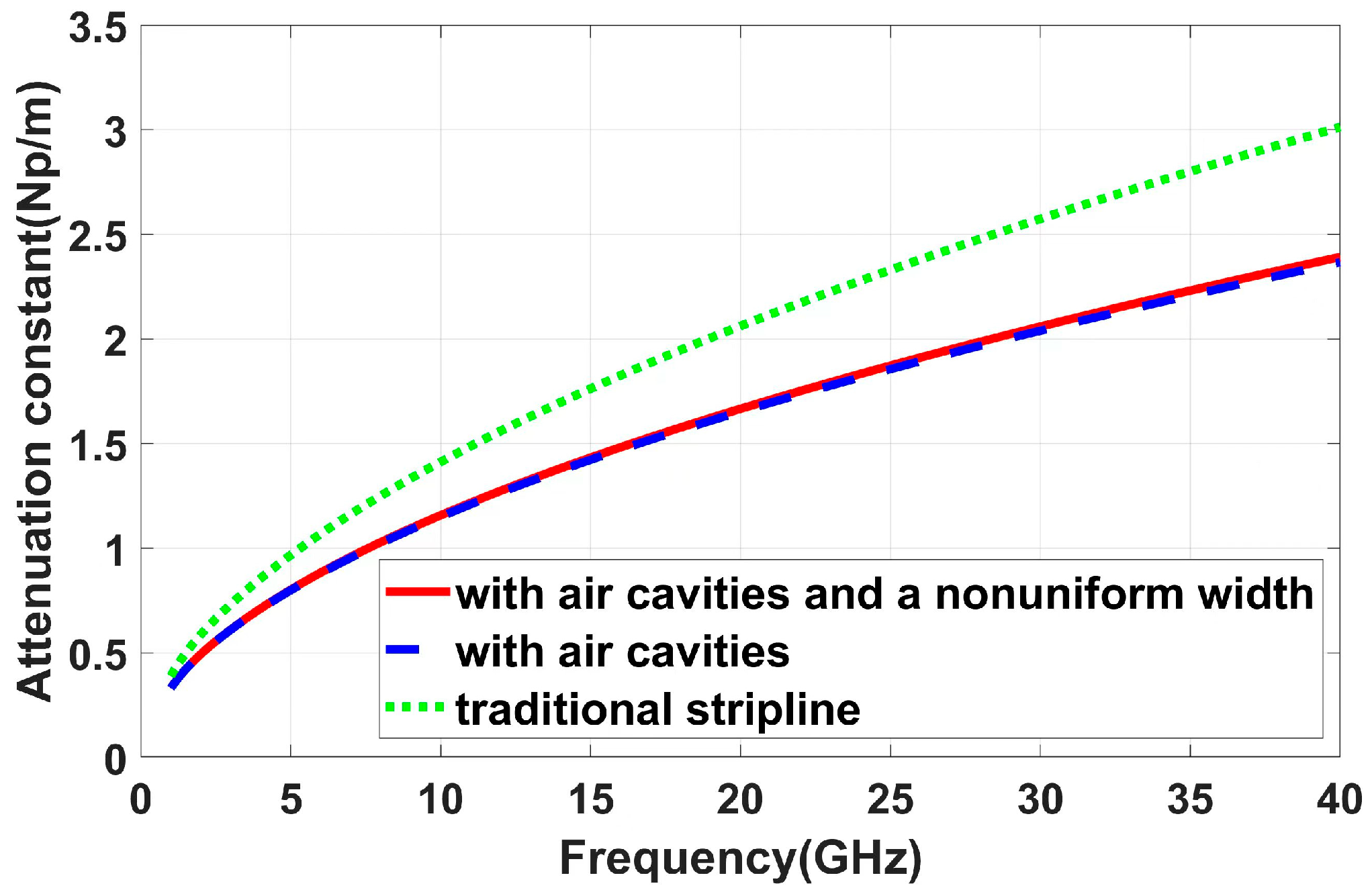
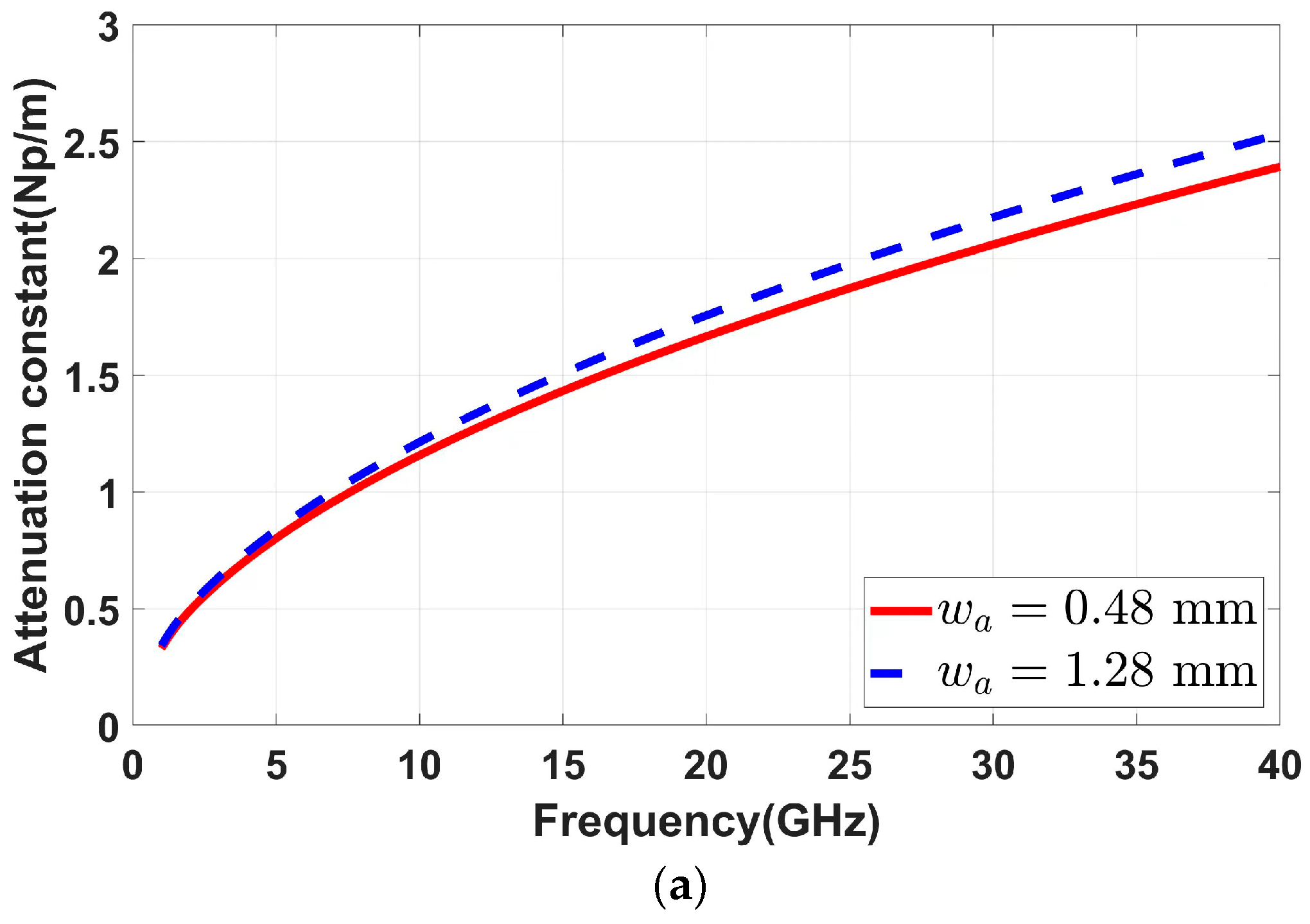
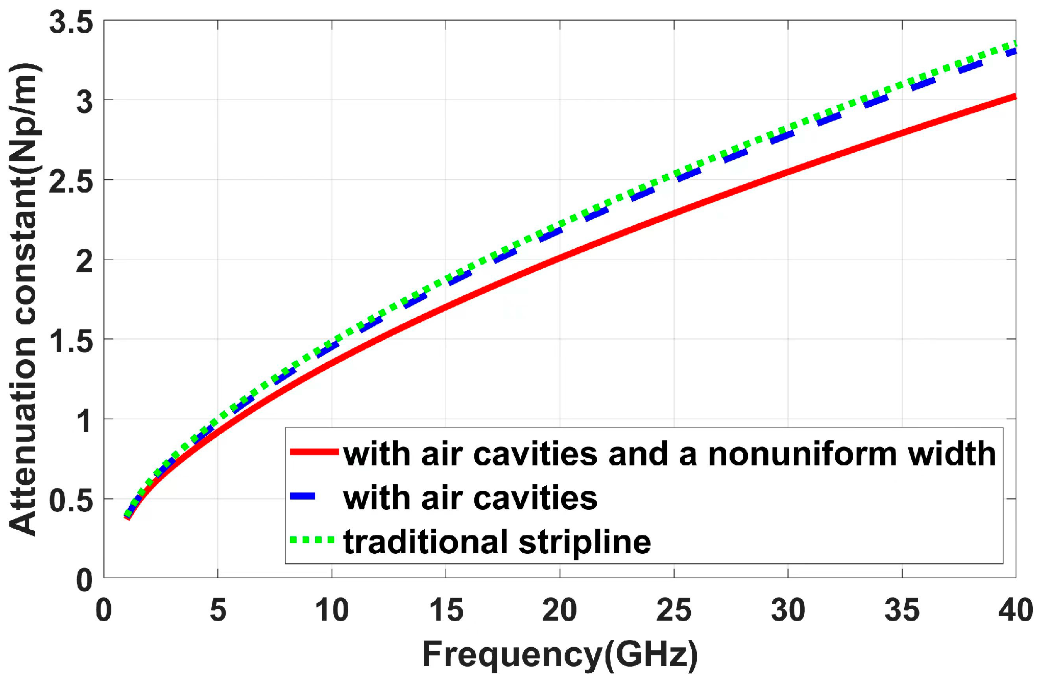
3.2.1. Loss Reduction

The attenuation constant of the stripline incorporating the proposed design methodology, along with its counterparts, is shown in Figure 8. The introduction of air cavities results in an average reduction of 19.40% in attenuation across the frequency band from DC to 40 GHz.

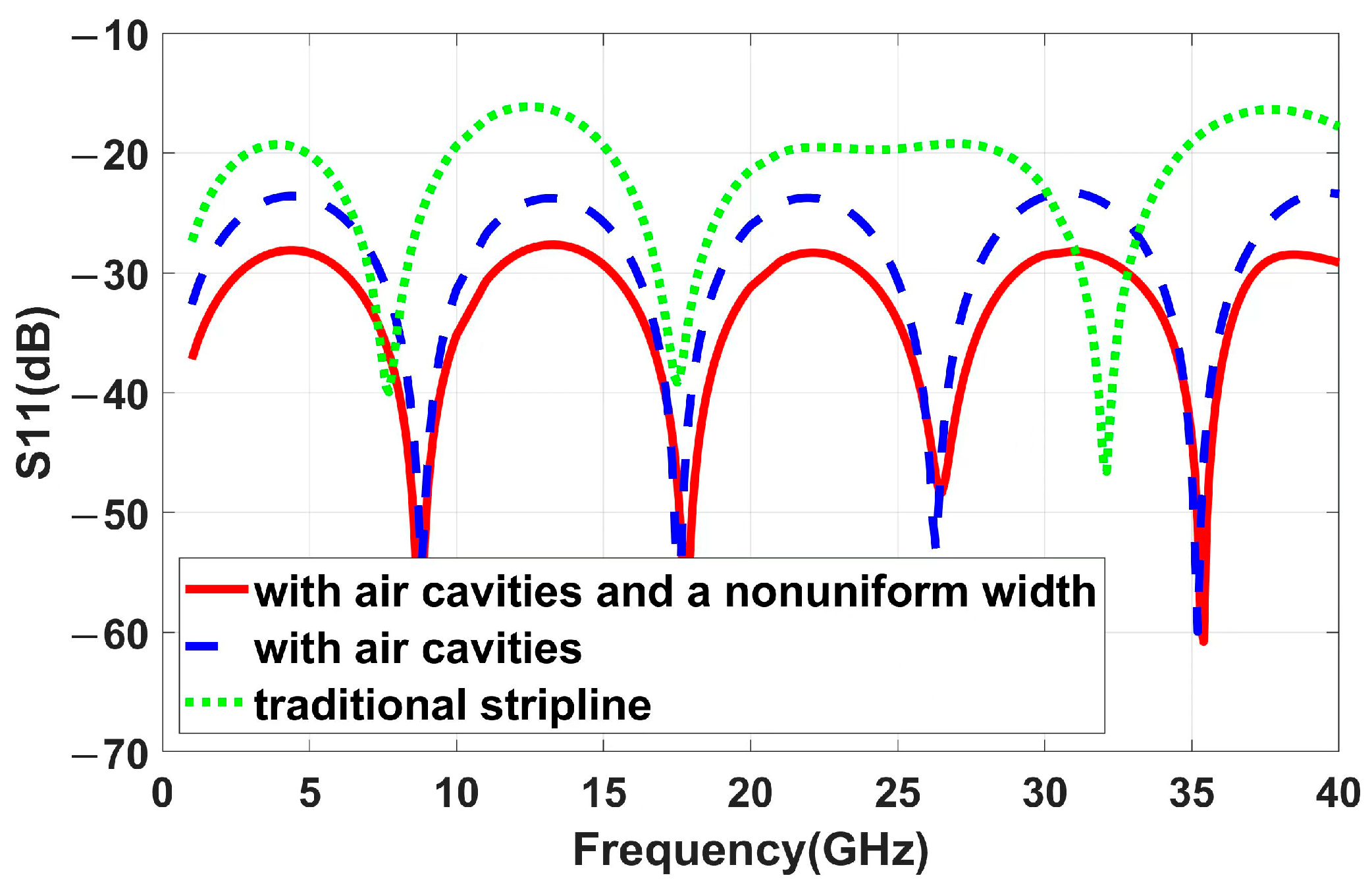
3.2.2. Improvement in Impedance Matching

The return loss of the stripline is shown in Figure 9. Using the proposed design methodology, the S11 is below −28 dB across the frequency band from DC to 40 GHz. By incorporating the air cavities and nonuniform-width conductor, the return loss is reduced by 11 dB compared to the traditional stripline and by 4 dB compared to the stripline with only air cavities.

3.2.3. The Optimal Design of the Density of Air Cavities

For the proposed design methodology, the density of air cavities is directly related to the reduction in loss. To investigate this relationship, results for different values of sa are compared, while keeping other parameters constant, as shown in Figure 10a,b. It can be observed that when sa increases from 0.3 mm to 0.6 mm, the return loss improves by an average of 6 dB, while the attenuation constant slightly deteriorated by 3.84% on average. This suggests that denser air cavities further reduce the equivalent loss tangent, although sparser cavities offer the advantage of an improved return loss due to fewer discontinuities in the transmission line. Therefore, a compromise between cavity density and fabrication constraints is recommended. Additionally, it is noteworthy that doubling sa results in only a slight variation in the performance, indicating that the proposed design methodology has a broad fabrication tolerance, making it suitable for implementation with many standard processes.

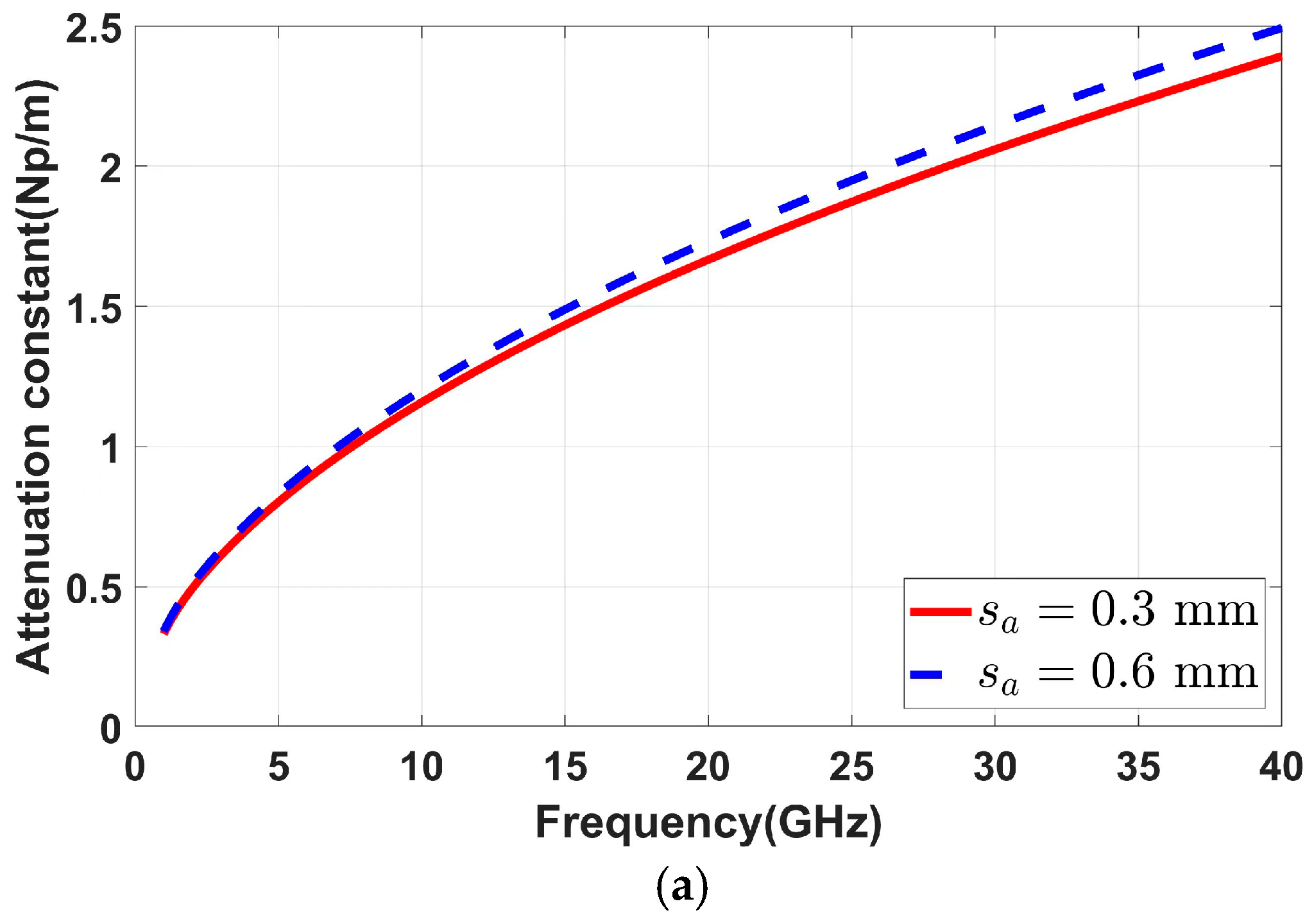
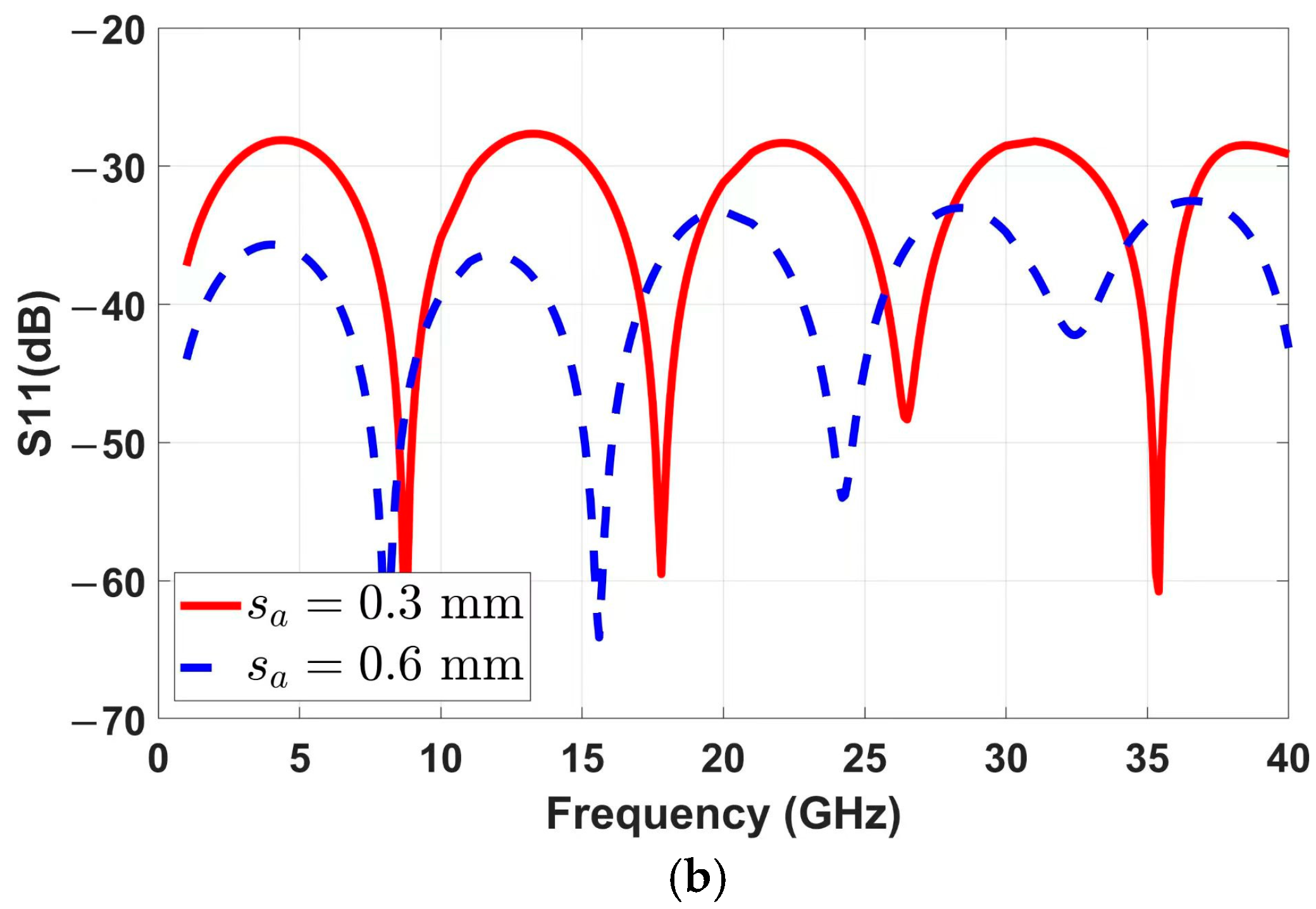
3.2.4. Process Tolerance of the Distance Between the Air Cavities and the Metal Line

Taking into account the feasibility of fabrication, it is known that the LTCC process allows for the fabrication of cavities within multilayer structures [31]. Considering factors such as alignment accuracy, material shrinkage rate, and thermal stress in the process, a minimum distance requirement between cavities and metal lines is necessary to prevent short circuits or open circuits. Increasing the distance between cavities and metal lines can enhance the reliability of the circuit. To evaluate the impact of this distance on the performance of the transmission line, wa is increased from 0.48 mm to 1.28 mm, equivalent to the distance increasing from 23.5 μm to 423.5 μm. This variation far exceeds the typical processing tolerance of LTCC technology (±15 μm). Keeping all the other parameters constant, the results are shown in Figure 11. In Figure 11a, when wa increases from 0.48 mm to 1.28 mm, a 5.14% deterioration in the attenuation constant is observed. This is due to the electromagnetic field distribution, which is concentrated near the metal line. As the distance between the air cavities and the metal line increases, the loss reduction becomes less pronounced. In contrast, Figure 11b shows a 2 dB decrease in S11 as wa changes from 0.48 mm to 1.28 mm, indicating only a slight variation. This is attributed to the fact that as the air cavities are moved farther from the metal line, the impedance mismatch caused by the cavities is reduced. Overall, the comparison suggests that the proposed design is not highly sensitive to changes in wa, as significant variations in wa result in only minor performance changes. Consequently, the design offers wide process tolerance and can be implemented using various manufacturing processes.

3.2.5. Study on the Applicability of the Methodology

To validate the effectiveness of the proposed methodology, it was applied to striplines fabricated on a Rogers 5880 (Rogers, Chandler, AZ, USA) substrate with the following parameters: b = 0.19 mm, bmax = 0.192 mm, da = 0.2 mm, h = 0.128 mm, l = 8 mm, sa = 0.4 mm, wa = 0.48 mm. For the simulations, a relative permittivity of εᵣ = 2.2 and a loss tangent of 0.0009 were assumed. As shown in Figure 12, the attenuation constant of the stripline implemented with the proposed methodology is reduced by 9.89% compared to the traditional design. These results demonstrate the notable adaptability of the proposed methodology.

4. Discussion

The comparison results demonstrate that the incorporation of air cavities effectively reduces the equivalent loss tangent, resulting in a significant decrease in overall loss. Additionally, the use of a periodically nonuniform-width inner conductor compensates for the impedance mismatches introduced by the air cavities, thereby further improving the return loss. This design methodology is validated through its application to both an SICL and a stripline. Moreover, the methodology can be extended to other interconnects in integrated circuits, utilizing standard fabrication processes with wide tolerance. Ultimately, the proposed interconnect design holds substantial potential for reducing power consumption in integrated circuits, offering a promising solution for improving performance in high-frequency applications.

5. Patents

A patent resulting from the work reported in this manuscript has been applied for, with the application number 202411724717.0.

Author Contributions

Conceptualization, Y.S.; methodology, Y.S.; software, M.Z.; validation, Y.S.; formal analysis, M.Z.; investigation, Y.S.; resources, Y.S.; data curation, M.Z; writing—original draft preparation, Y.S.; writing—review and editing, Y.S.; visualization, M.Z.; supervision, Y.S.; project administration, Y.S.; funding acquisition, Y.S. All authors have read and agreed to the published version of the manuscript.

Funding

This research was funded by the National Natural Science Foundation of China under Grant number 62101332.

Institutional Review Board Statement

Not applicable.

Informed Consent Statement

Not applicable.

Data Availability Statement

Data are contained within the article.

Conflicts of Interest

The authors declare no conflicts of interest.

References

  1. Kissinger, D.; Kaynak, M.; Mai, A. Integrated millimeter-wave and terahertz analyzers for biomedical applications. IEEE Trans. Microw. Theory Tech. 2022, 70, 5141–5158. [Google Scholar] [CrossRef]
  2. Piovesan, T.; Prado, E.; Sartori, H.C.; Pinheiro, J.R. Analytical electro-thermal model and 3-D thermal resistance network for SMD-based printed circuit board power converters. IEEE J. Emerg. Sel. Top. Power Electron. 2024, 12, 4979–4992. [Google Scholar] [CrossRef]
  3. Min, Q.; Li, E.-P.; Jin, J.-M.; Chen, W. Electrical–thermal cosimulation of coaxial TSVs with temperature-dependent MOS effect using equivalent circuit models. IEEE Trans. Electromagn. Compat. 2020, 62, 2247–2256. [Google Scholar] [CrossRef]
  4. Köroğlu, Ç.; Pop, E. High thermal conductivity insulators for thermal management in 3D integrated circuits. IEEE Electron Device Lett. 2023, 44, 496–499. [Google Scholar] [CrossRef]
  5. Helou, A.; Venugopal, A.; Raad, P.E. Compact 3D thermal model for VLSI and ULSI interconnect network reliability verification. IEEE Trans. Device Mater. Reliab. 2021, 21, 240–251. [Google Scholar] [CrossRef]
  6. Nericua, R.; Wang, K.; Zhu, H.; Gómez-García, R.; Zhu, X. Low-loss and compact millimeter-wave silicon-based filters: Overview, new developments in silicon-on-insulator technology, and future trends. IEEE J. Emerg. Sel. Top. Circuits Syst. 2024, 14, 30–40. [Google Scholar] [CrossRef]
  7. Li, C.-H.; Chiu, T.-Y. Low-loss single-band, dual-band, and broadband mm-wave and (sub-)THz interconnects for THz SoP heterogeneous system integration. IEEE Trans. Terahertz Sci. Technol. 2022, 12, 130–143. [Google Scholar] [CrossRef]
  8. Pfahler, T.; Scheder, A.; Bridier, A.; Schür, J.; Vossiek, M. A low-loss bond-wire interconnect design with more than 130 GHz bandwidth enabling an ultra-broadband heterogeneous system design. IEEE Trans. Microw. Theory Tech. 2024, 72, 505–515. [Google Scholar] [CrossRef]
  9. Yu, B.; Liu, Y.; Ye, Y.; Liu, X.; Gu, Q.J. Low-loss and broadband G-band dielectric interconnect for chip-to-chip communication. IEEE Microw. Wirel. Compon. Lett. 2016, 26, 478–480. [Google Scholar] [CrossRef]
  10. Khac Le, H.; Kim, S. Machine Learning Based Energy-Efficient Design Approach for Interconnects in Circuits and Systems. Appl. Sci. 2021, 11, 915. [Google Scholar] [CrossRef]
  11. Gatti, F.; Bozzi, M.; Perregrini, L.; Wu, K.; Bosisio, R.G. A novel substrate integrated coaxial line (SICL) for wide-band applications. In Proceedings of the 2006 European Microwave Conference, Manchester, UK, 10–15 September 2006. [Google Scholar]
  12. Xu, F.; Wu, K. Guided-wave and leakage characteristics of substrate integrated waveguide. IEEE Trans. Microw. Theory Tech. 2005, 53, 66–73. [Google Scholar]
  13. Wu, K.; Bozzi, M.; Fonseca, N.J.G. Substrate integrated transmission lines: Review and applications. IEEE J. Microw. 2021, 1, 345–363. [Google Scholar] [CrossRef]
  14. Kim, M.; Bae, B.; Cheon, J. Experimental characterization of millimeter-wave substrate-integrated waveguide interconnect with slot transition in flexible printed circuit boards. Electronics 2022, 11, 2995. [Google Scholar] [CrossRef]
  15. Nwajana, A.O.; Obi, E.R. A review on SIW and its applications to microwave components. Electronics 2022, 11, 1160. [Google Scholar] [CrossRef]
  16. Lu, C.; Yang, L.; Yin, X.; Zhao, H.; Liu, L. Very low crosstalk measurement of substrate integrated coaxial line (SICL). Electronics 2019, 8, 1174. [Google Scholar] [CrossRef]
  17. Shao, Y.; Li, X.-C.; Wu, L.-S.; Mao, J.-F. A wideband millimeter-wave substrate integrated coaxial line array for high-speed data transmission. IEEE Trans. Microw. Theory Tech. 2017, 65, 2789–2800. [Google Scholar] [CrossRef]
  18. Ning, K.; Li, X.C.; Shao, Y.; Mao, J.F. Low-loss wide-bandwidth planar transmission line with a laminated conductor. Sci. China Inf. Sci. 2023, 66, 152304. [Google Scholar] [CrossRef]
  19. Belenguer, A.; Borja, A.L.; Esteban, H.; Boria, V.E. High-performance coplanar waveguide to empty substrate integrated coaxial line transition. IEEE Trans. Microw. Theory Tech. 2015, 63, 4027–4034. [Google Scholar] [CrossRef]
  20. Isapour, A.; Kouki, A.B. Empty LTCC integrated waveguide with compact transitions for ultra-low loss millimeter-wave applications. IEEE Microw. Wirel. Compon. Lett. 2017, 27, 144–146. [Google Scholar] [CrossRef]
  21. Rehman, M.; Kumar, L.N.; Erdogan, V.S.; Swaminathan, M. Air-filled SIWs using laminate dielectrics on glass substrate for D-band applications. IEEE Trans. Compon. Packag. Manuf. Technol. 2024, 14, 98–105. [Google Scholar] [CrossRef]
  22. Sun, C.-S.; Li, X.-C.; Zhan, H.-B.; Ning, K. A low-loss and high-bandwidth hollow rectangular dielectric waveguide for sub-THz applications. IEEE Trans. Microw. Theory Tech. 2024, 72, 5961–5969. [Google Scholar] [CrossRef]
  23. Noguchi, J.; Sato, K.; Konishi, N.; Uno, S.; Oshima, T.; Ishikawa, K.; Ashihara, H.; Saito, T.; Kubo, M.; Tamaru, T.; et al. Process and reliability of air-gap Cu interconnect using 90-nm node technology. IEEE Trans. Electron Devices 2005, 52, 352–359. [Google Scholar] [CrossRef]
  24. Noguchi, J.; Oshima, T.; Matsumoto, T.; Uno, S.; Sato, K. Multilevel interconnect with air-gap structure for next-generation interconnections. IEEE Trans. Electron Devices 2009, 56, 2675–2682. [Google Scholar] [CrossRef]
  25. Spencer, T.J.; Joseph, P.J.; Kim, T.H.; Swaminathan, M.; Kohl, P.A. Air-gap transmission lines on organic substrates for low-loss interconnects. IEEE Trans. Microw. Theory Tech. 2007, 55, 1919–1925. [Google Scholar] [CrossRef]
  26. Kumar, V.; Sharma, R.; Uzunlar, E.; Zheng, L.; Bashirullah, R.; Kohl, P.; Bakir, M.S.; Naeemi, A. Airgap interconnects: Modeling, optimization, and benchmarking for backplane, PCB, and interposer applications. IEEE Trans. Compon. Packag. Manuf. Technol. 2014, 4, 1335–1346. [Google Scholar] [CrossRef]
  27. Green, H.E. Conductor geometry independence of phase velocity in TEM-mode transmission lines. IEEE Trans. Microw. Theory Tech. 1989, 37, 805. [Google Scholar] [CrossRef]
  28. Wilcoxon, R. The effects of geometry and dielectric material on stripline and microstrip internal temperatures. IEEE Trans. Compon. Packag. Technol. 2005, 28, 674–679. [Google Scholar] [CrossRef]
  29. Liu, X.; Zhu, Y.; Yang, Y.; Ding, R. Low-loss air-cavity through-silicon vias (TSVs) for high speed three-dimensional integrated circuits (3-D ICs). IEEE Microw. Wirel. Compon. Lett. 2016, 26, 89–91. [Google Scholar] [CrossRef]
  30. A6M/A6M-E High Frequency LTCC Tape System. Available online: http://www.ferro.com/Our+Products/ColorsGlass/Electronic/Electronic-Materials/docs/A6M%20A6M-E%20LTCC%20Tape%20System.pdf (accessed on 1 January 2017).
  31. Kumar, A.; Viswambharaet, P.; Surendranath, K.; Srivastava, P.K.; Chaturvedi, I.; Singh, H.; Prajapati, K.; Parmar, H.; Naranbhai, L.R.; Sinha, S.; et al. Defect free lamination of low temperature co-fired ceramic multi-chip-modules. In Proceedings of the 2024 International Conference on Integrated Circuits, Communication, and Computing Systems, Una, India, 8–9 June 2024. [Google Scholar]
Figure 1. Structure of an SICL.
Applsci 15 02799 g001
Figure 2. An SICL with two rows of periodic cylindrical air cavities.
Applsci 15 02799 g002
Figure 3. Profile of an SICL with two rows of periodically arranged cylindrical air cavities, viewed from the longitudinal section Y0: (a) overall view; (b) vertical view.
Applsci 15 02799 g003
Figure 4. Profile of an SICL with two rows of periodic cylindrical air cavities and a nonuniform-width inner conductor with periodic variations, viewed from the longitudinal sectionY0: (a) overall view; (b) vertical view.
Applsci 15 02799 g004
Figure 5. The supporting structure.
Applsci 15 02799 g005
Figure 6. Attenuation constant comparison for the SICL.
Applsci 15 02799 g006
Figure 7. Return loss comparison for the SICL.
Applsci 15 02799 g007
Figure 8. Attenuation constant comparison for the stripline.
Applsci 15 02799 g008
Figure 9. Return loss comparison for the stripline.
Applsci 15 02799 g009
Figure 10. Comparison of different air cavity densities: (a) attenuation constant; (b) return loss.
Applsci 15 02799 g010aApplsci 15 02799 g010b
Figure 11. Comparison of different distances between the air cavities and the metal line: (a) attenuation constant; (b) return loss.
Applsci 15 02799 g011aApplsci 15 02799 g011b
Figure 12. Comparison of the attenuation constants of striplines on Rogers 5880 substrate.
Applsci 15 02799 g012
Table 1. Dimensional parameters of the implementation used in the validation (Unit: mm).
abbmaxddahlssawa
SICL1.170 0.12 0.175 0.15 0.2 0.192 15.22 0.3 0.3 0.39
stripline-0.1930.233-0.20.2958-0.30.48
Disclaimer/Publisher’s Note: The statements, opinions and data contained in all publications are solely those of the individual author(s) and contributor(s) and not of MDPI and/or the editor(s). MDPI and/or the editor(s) disclaim responsibility for any injury to people or property resulting from any ideas, methods, instructions or products referred to in the content.

