Abstract
As the demand for high-density integrated circuits increases, scaling down devices has already reached its limit, making the optimization of interconnect–via layout an important research challenge. Conventional semiconductor design adopts conservative margins to ensure process reliability, but this often results in inefficient space utilization and degraded electrical performance. This study evaluates the possibility of optimizing design rules by analyzing the impact of reduced contact area in interconnect–via structures on the current flow and resistance. Finite element method analysis (FEM) using Ansys Workbench revealed that current is concentrated in approximately 20% of the interconnect height and the diagonal region of the via. A resistance model reflecting this current distribution demonstrated high accuracy, with an error range of 1–3% compared to simulation results. Resistance measurements of various fabricated structures produced through photolithography and lift-off processes showed a significant increase in resistance when the contact area was reduced to 50% or less, consistent with simulation results. This study demonstrates the potential to optimize both space utilization and electrical performance by minimizing the conservative margins between interconnects and vias, contributing to next-generation high-density integrated circuit design.
1. Introduction
For decades, the semiconductor industry has advanced through continuous process scaling, maximizing performance by reducing transistor sizes and increasing integration density [1]. The core strategy of semiconductor technology development has been to shrink transistors and enhance integration, leading to improvements in processing speed, power efficiency, and the miniaturization of devices. However, as Moore’s Law approaches its physical limits, it is becoming increasingly difficult to sustain performance improvements solely through device scaling [2,3,4]. Additionally, challenges such as signal delay, increased power consumption, and heat dissipation have intensified, necessitating new approaches to semiconductor design optimization. Against this backdrop, recent semiconductor technology development has shifted focus beyond simple transistor scaling toward performance enhancement through interconnect and layout optimization [5,6]. While previous research primarily concentrated on improving transistor performance, inefficient interconnect structures can severely limit the overall system efficiency, regardless of individual transistor advancements. Optimizing interconnect structures with respect to signal transmission characteristics and the current flow has become a critical research area for improving semiconductor device performance.
In particular, optimizing semiconductor interconnects and via structures is a key factor directly influencing chip performance and integration density. Interconnects play a crucial role in transmitting signals between transistors, while vias provide electrical pathways between different metal layers [7]. Consequently, the dimensions and placement of interconnects and vias significantly affect the electrical performance and reliability of integrated circuits [8]. Traditionally, semiconductor design methodologies have maintained sufficient contact area between interconnects and via while incorporating generous margins to compensate for potential misalignment and process variations.
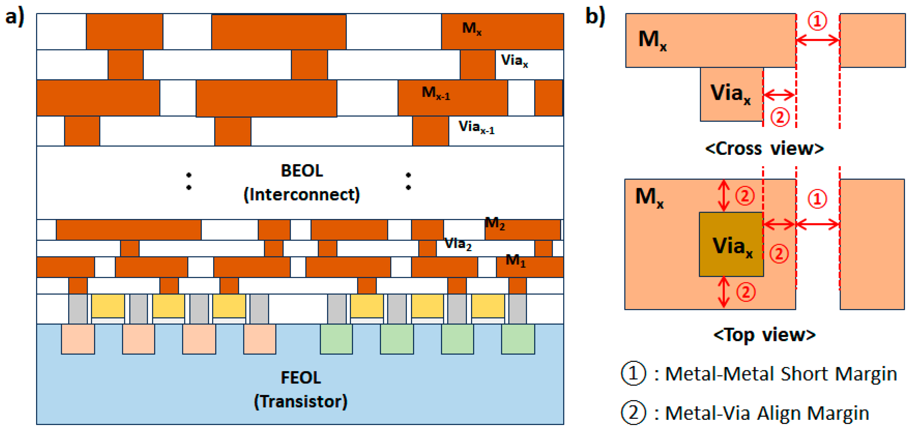
Figure 1a shows the cross-section of a semiconductor system structure. The Front-end of line (FEOL) region consists of unit devices, while the Back-end of line (BEOL) region is composed of interconnects that implement circuits and vias that connect the wiring layers. The dimensions and shapes of interconnects and vias, commonly referred to as design rules, are determined by considering unit process capabilities such as patterning and deposition. For example, the spacing between adjacent metal lines must account for patterning margins from processes like photolithography and etching to prevent shorts. Similarly, vias must be placed correctly within metal lines, considering photo alignment margins between each layer to ensure proper positioning.
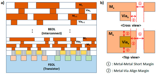
Figure 1.
(a) Cross-section of the semiconductor system structure and FEOL/BEOL regions, (b) top and cross views of the metal and via forming the interconnect, and layout constraints considering short and alignment margins.
Figure 1b illustrates a layout that reflects these margins, showing that metal lines are spaced apart to accommodate patterning margins and vias are positioned with sufficient gaps within the metal lines for proper alignment. These layout margins enhance manufacturing reliability but also consume valuable layout space, thereby limiting integration density [9]. Larger margins increase interconnect spacing, reducing the number of interconnects that can be accommodated within a given area. As interconnect lengths increase, signal transmission paths become longer, leading to greater signal delay, higher power consumption, and uneven current density distribution. As conventional process scaling reaches its limits, semiconductor technology is evolving toward performance enhancement through interconnect and via structure optimization [10]. Recent studies suggest that precisely analyzing the signal transmission characteristics of interconnects and vias can reduce unnecessary margins, enabling more efficient layout designs [11,12]. This study also aims to propose a method for efficient layout design by eliminating unnecessary margins based on quantitative analysis of the current flow. Additionally, the main body of this paper is divided into five distinct sections: the Section 2 discusses analysis using the FEM approach; the Section 3 outlines the process of developing mathematical models based on the simulation results; the Section 4 describes experiments conducted to validate these models; the Section 5 interprets and analyzes the experimental outcomes; and finally, the Section 6 summarizes the overall findings and implications of this study.
2. Simulation
To optimize the performance of semiconductor chips, it is essential to conduct a detailed analysis of the structural characteristics of interconnects and vias and derive a design that maximizes current transfer efficiency. This study analyzes the impact of via geometry (length and width) on resistance and current density in metal line–via–metal line structures and investigates the feasibility of reducing the design margin between interconnects and vias. To achieve this, FEM-based simulations were performed using the Ansys Simulation Tool, and the current flow was analyzed under various via structures and misalignment conditions [13]. Although various analytical methods, such as the Monte Carlo approach, are available for analyzing semiconductor structures, the FEM uniquely segments structures into finely divided elements and precisely incorporates conditions for each segment and boundary. Therefore, we determined that the FEM is the most suitable method for accurately capturing detailed current flow patterns within interconnect structures. First, a precise analysis was conducted on how variations in via dimensions and reductions in the interconnect–via contact area affect resistance and current density distribution using FEM-based simulations. The simulations were carried out using Ansys Workbench, and a mesh size of 1 µm was applied to determine the resolution of the analysis model for accurate current density distribution and resistance values [14]. If the mesh size is too large, changes in current density may not be properly reflected, reducing the reliability of the analysis results. Therefore, to accurately analyze the regions where current is concentrated inside the via, an appropriate mesh size of 1 µm was chosen. The voltage was applied horizontally at 3 V, modeling a structure where current flows from a metal interconnect through the via and back into the interconnect.
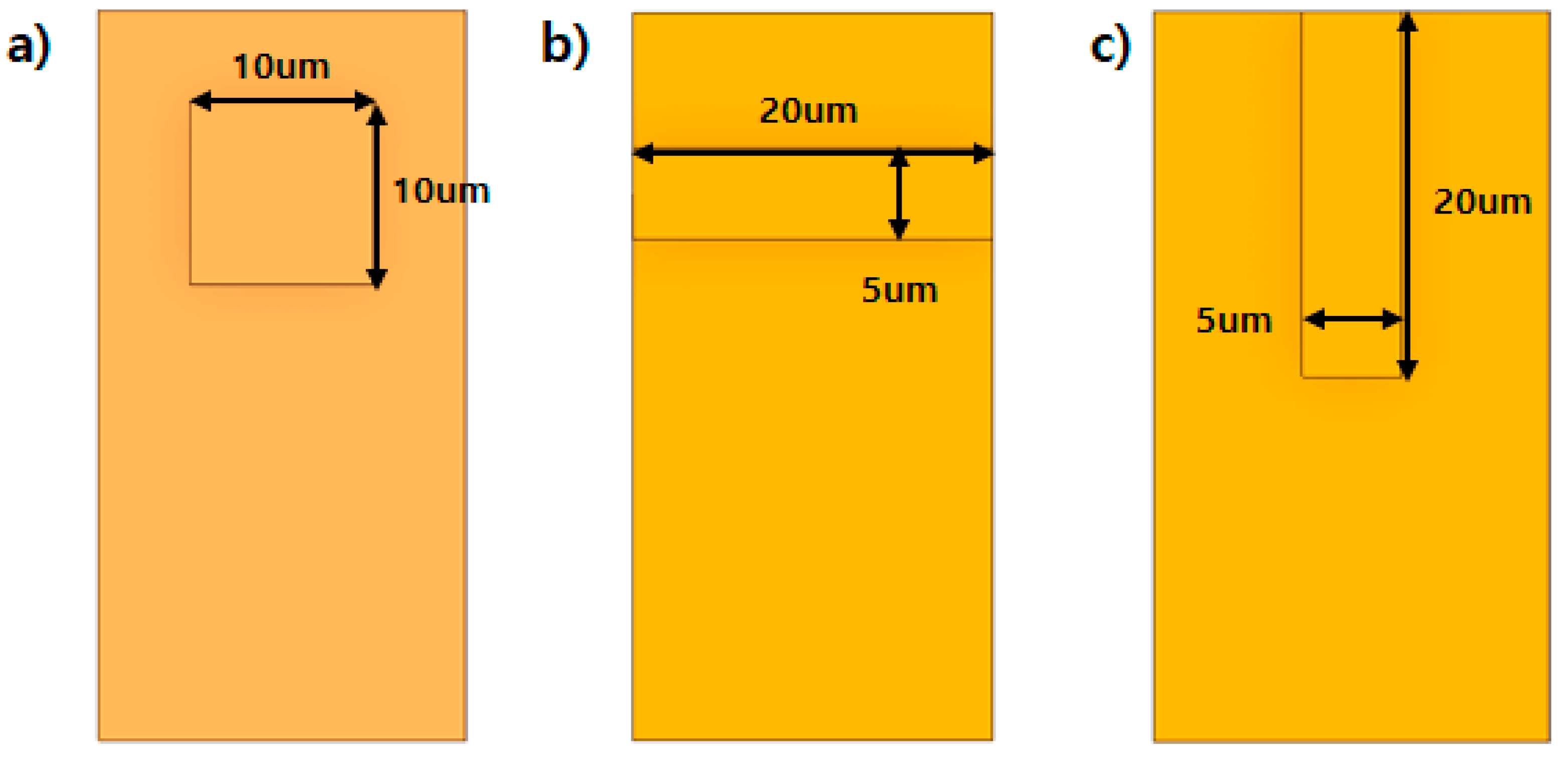
To examine the impact of via structure variations on resistance, three different structures were investigated. The upper and lower interconnects each have a length of 40 µm and a width of 20 µm. Three different via structures were inserted between them for analysis. The current was applied such that it flowed through the upper interconnect, passed through the via, and then continued through the lower interconnect. A reference structure (10 µm × 10 µm) was compared with two additional structures: (20 µm × 5 µm), where current encounters the via the fastest, and (5 µm × 20 µm), where current encounters the via the slowest. This approach aims to clearly identify the impact of via geometry by ensuring that the current flow direction and via area remain identical, eliminating any variations in current density that might arise solely from area differences. Figure 2a–c illustrate the via structures, which were designed with dimensions of 10 × 10 µm, 5 × 20 µm, and 20 × 5 µm, respectively.
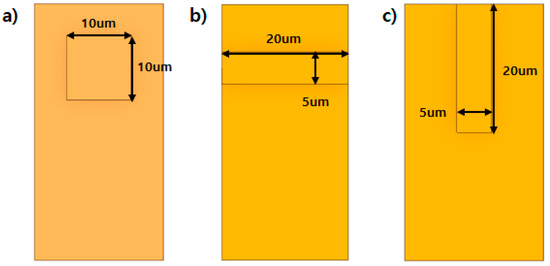
Figure 2.
Via structures with identical area (100 µm2) but different dimensions: (a) 10 µm × 10 µm, (b) 20 µm × 5 µm, and (c) 5 µm × 20 µm.
All structures maintain an identical area of 100 µm2 to minimize differences in current density and isolate the effects of shape on resistance. If the total via area varied, the overall current-carrying capacity of the via would change, potentially altering the distribution of current density. Therefore, by keeping the area constant while adjusting the length-to-width ratio, this study aims to clearly compare the relationship between the current flow direction and via shape and quantitatively evaluate its impact on resistance.
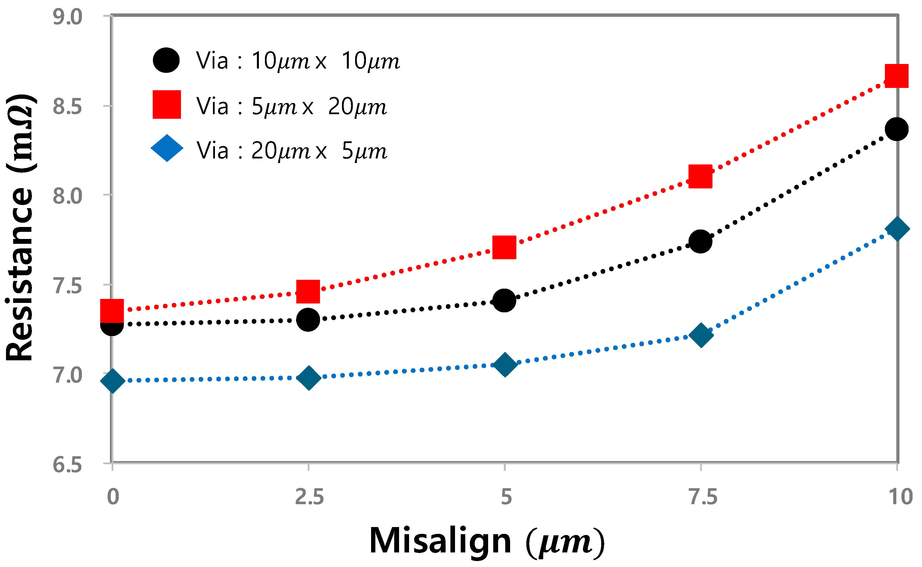
The simulation results in Figure 3 reveal that the highest total resistance was observed in the (5 × 20 µm) structure (Figure 2b), whereas the lowest resistance was found in the (20 × 5 µm) structure (Figure 2c). These results indicate that increasing the via length in the direction of the current flow reduces resistance. This finding highlights the significant influence of the via length-to-width ratio on resistance and suggests that extending the via length parallel to the current flow while reducing its width is an effective strategy for resistance reduction.
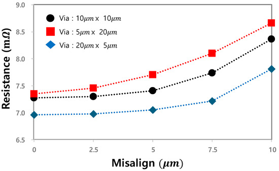
Figure 3.
Total resistance as a function of misalignment for different via structures: 10 µm × 10 µm, 5 µm × 20 µm, and 20 µm × 5 µm.
These results indicate that even when the via area is the same, the current density is not uniform. If the current density were uniform, there would be no difference in resistance values. Therefore, the difference in current density suggests that charge does not distribute evenly within the via region. To verify this, simulations were also conducted to analyze resistance variations by changing the interconnect–via contact area (in this study, by gradually reducing the contact area to simulate increasing misalignment). The misalignment condition was implemented by shifting the upper metal interconnect in 2.5 µm increments, gradually reducing its contact area with the via, and analyzing the total resistance under these conditions. According to the simulation results in Figure 3, resistance remained relatively stable, with a variation of less than 3%, up to a misalignment of 5 µm. However, beyond this point, as the contact area decreased further, the resistance increased sharply. Additionally, the structure with a larger initial resistance—where the via was elongated in the transverse direction (resulting in a longer current path through the via)—exhibited a more significant increase in resistance. These results indicate that insufficient contact area leads to electrical performance degradation, and the extent of this degradation is also influenced by the shape of the via.
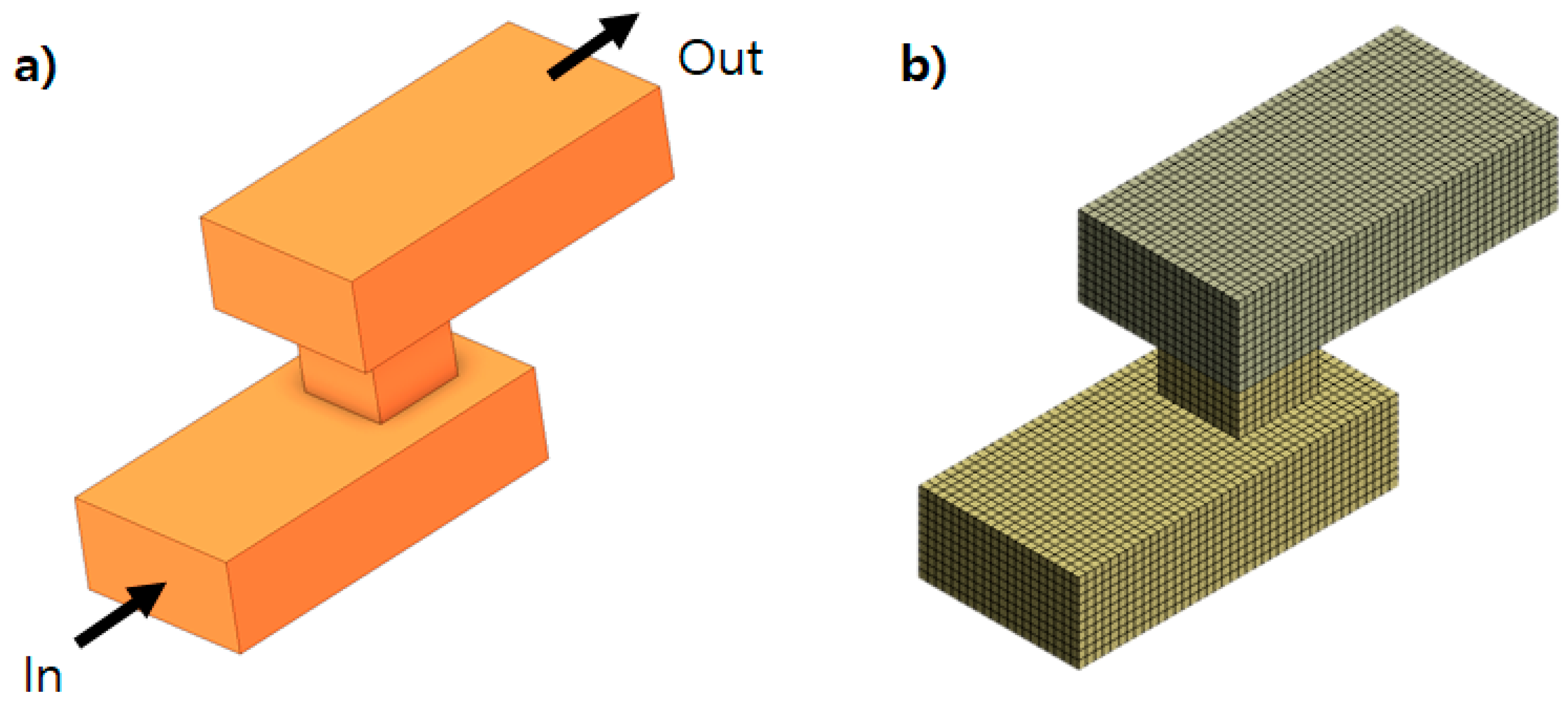
Additional simulations were performed to examine the distribution of current density and analyze conditions where the interconnect-to-via contact area decreases due to misalignment. Using the same settings as in the previous Ansys Workbench simulations, a 3 V horizontal voltage was applied to model the current flow from the interconnect through the via and back to the interconnect, as shown in Figure 4a. The mesh size was set to 1 µm to maintain high simulation accuracy, as depicted in Figure 4b. The simulated structures were based on Figure 2a,b, with contact area reductions ranging from fully overlapped to 90% misaligned. The impact of contact area variation on current density and resistance was then analyzed.

Figure 4.
(a) Simulation model with horizontal voltage input and current flow through the via. (b) Mesh with a 1 µm grid size.
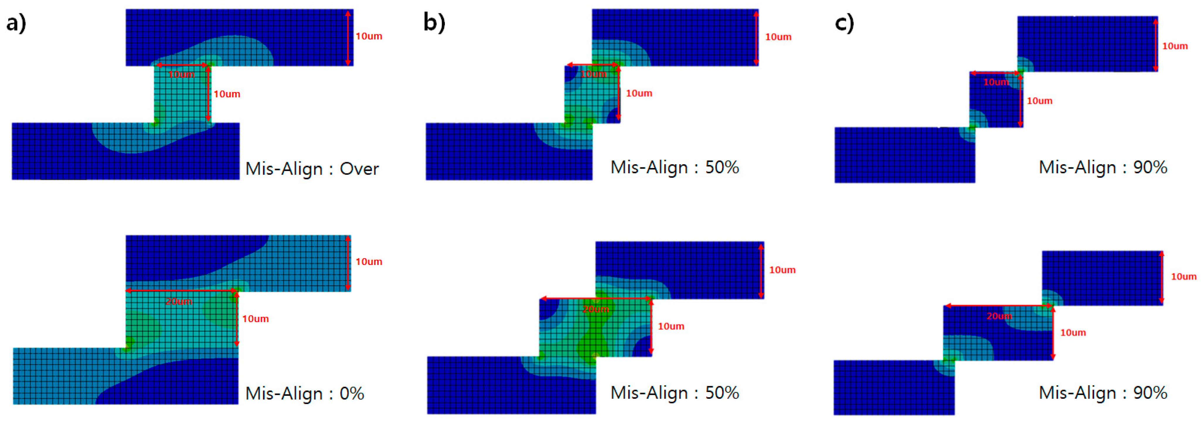
Based on the structure shown in Figure 4, the simulation was conducted, and the cross-sectional current distribution is presented in Figure 5. The simulation results indicate that current density flows along the metal interconnect and concentrates diagonally within the via after reaching it. Even as the contact area decreases, current density remains concentrated at the via-interconnect contact edges, suggesting that the primary current path through the diagonal via direction is maintained despite contact area reduction. Additionally, negligible current density was observed in interconnect regions that were not in contact with the via. This finding implies that unnecessary interconnect regions that do not contribute to the current flow can potentially be eliminated from the design. The analysis of current density flow patterns revealed that as the interconnect-to-via contact area decreases, current density within the via increases. However, the overall current flow pattern remains consistent. Current enters the via from the interconnect, flows diagonally within the via, and exits through the interconnect. Notably, even if the interconnect length is sufficiently long, current does not flow significantly in areas not directly contacting the via. This suggests that longer interconnects do not necessarily enhance current conduction efficiency and that current flows primarily through areas where interconnects are physically connected to the via.

Figure 5.
Current density distribution for via structures with misalignment conditions: (a) over-align, (b) 50% misalign, and (c) 90% misalign.
Based on these findings, it is concluded that minimizing the design margin between interconnects and vias is feasible. Conventional semiconductor layout designs typically allocate generous margins to account for process variations. However, this study demonstrates that unnecessary margins can be reduced without performance degradation by analyzing current density flow. Additionally, considering that current flows diagonally within the via, reducing the interconnect-to-via contact area does not significantly impact current transfer efficiency. The simulation results obtained in this study provide a foundation for modeling optimized interconnect and via structures using analytical equations. As the next step, simulation data will be analyzed to derive equations that quantitatively describe the current flow and resistance characteristics. These equations will then be utilized to propose design guidelines for layout optimization.
3. Formula
The analysis of the current flow path revealed that even when the length of the interconnect increases, the regions that do not come into contact with the via exhibit negligible current flow. This phenomenon occurs because, during the transition of current from the interconnect to the via and back to the interconnect, the segment of the interconnect outside the via contact area is effectively unused. Therefore, minimizing such unnecessary interconnect sections allows for a more compact layout design, contributing to reduced fabrication costs and enhanced electrical performance.
In this study, FEM simulations were employed to analyze the current density distribution in a metal line–via–metal line structure, and based on these results, an analytical equation for resistance was derived. Traditional electrical characteristic analyses typically estimate resistance by considering only the geometric structure of interconnects and vias. However, this study aims to present a more realistic resistance model by incorporating the effects of interconnect-to-via contact area on the current flow. The FEM simulation demonstrated that the current density tended to concentrate in specific regions, including approximately 20% of the interconnect height and the diagonal edges of the via. By evaluating the total resistance for specific via dimensions (10 × 10 µm) and (20 × 5 µm), this study established a generalized resistance equation that accounts for structural parameters. This equation was validated by applying it to various structures and comparing the computed resistance values with simulation results. Since resistance varies depending on the current flow path, the resistance equation was formulated to reflect the structural characteristics of interconnects and vias.
Figure 6a,b illustrate schematic diagrams for modeling the resistance equation considering current density. As shown in the simulation results and referenced in Figure 5, the current is concentrated along the surface of the interconnect in the direction of the current flow and along the diagonal direction of the via. Based on this observation, the resistance equation was modeled by assuming that current flows through 20% of the interconnect surface and the diagonal region of the via.
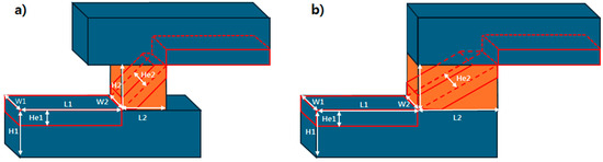
Figure 6.
3D model showing the geometric parameters for resistance calculation (a) 10 μm × 10 μm, (b) 20 μm × 5 μm.
The fundamental resistance equation is typically given as [15]. However, in real structures, the actual cross-sectional area through which current flows is not simply the geometric cross-section but rather an effective cross-section where current density is concentrated. Accordingly, the resistance for interconnects and vias was expressed using the following models where is the interconnect length in the direction of the current flow, is the interconnect width, is the effective height where the current density is concentrated, and A is a coefficient reflecting the current distribution in the interconnect. The effective height was derived considering that only about 20% of the interconnect’s height contributes to significant current flow. For the via, current does not flow strictly vertically but rather diagonally. To account for this, the effective current path length was set as .
Moreover, the effective current flow cross-section was considered by dividing the effective length by , incorporating the concentration of current along the diagonal direction. The term was introduced to correct for changes in current density when the via width varies, where is the reference interconnect width. Additionally, the terms , were included to reflect the current flow directions within the via. This approach allowed for a more precise resistance model by incorporating both the concentrated current density region and the current flow direction. The coefficients A and B are constants that reflect additional characteristics of the interconnect and via, respectively. Consequently, the total resistance (R total) can be defined as in Equation (1), and the constant values used in Equation (1) are additionally presented in Equations (2) and (3). In summary, the resulting equation from the modeling is as follows:
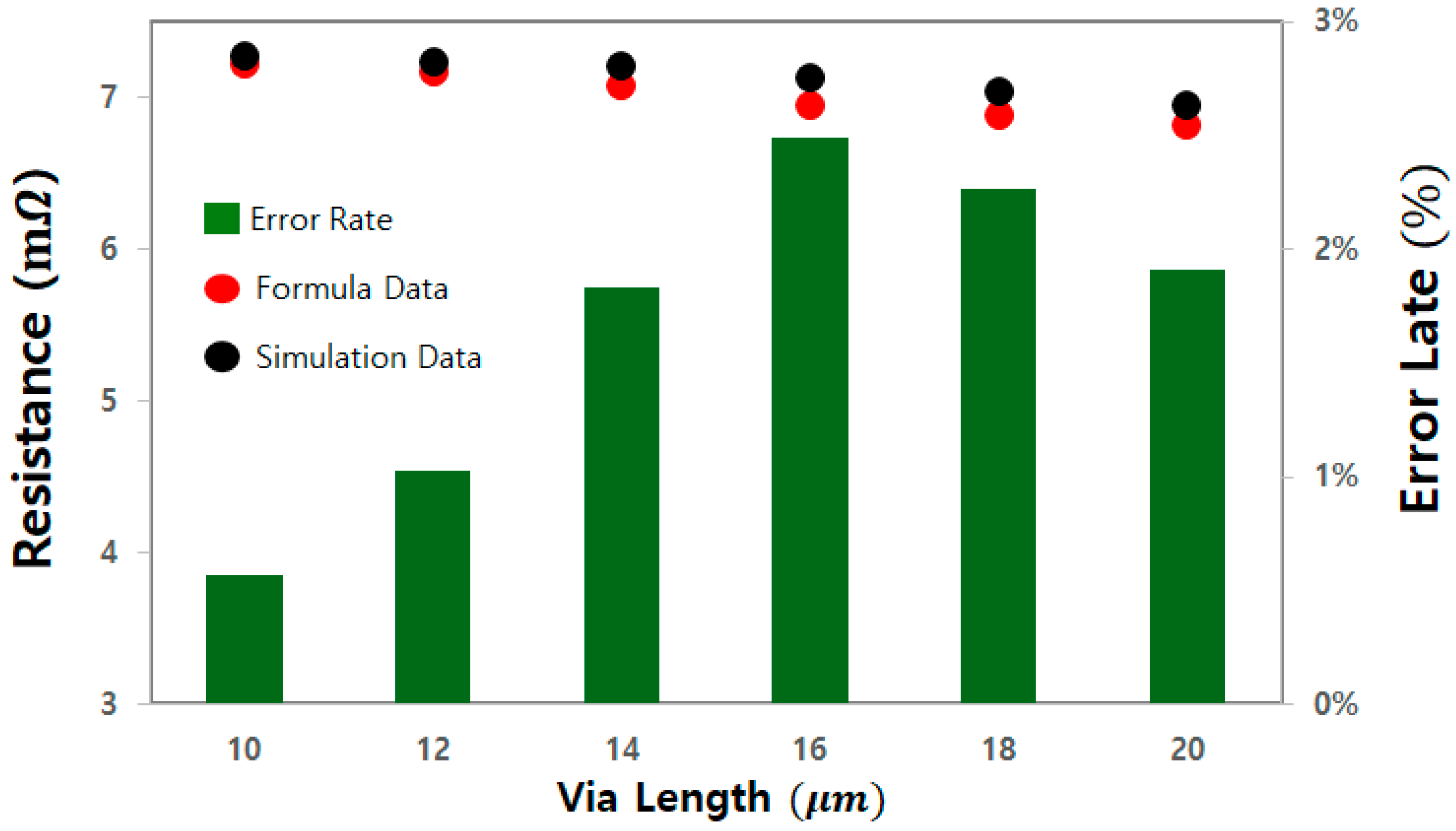
Figure 7 shows the results of recalculating and comparing the simulation results by applying the modeling equation to each via dimension. The error rate between the computed and simulated resistance values remained below 3% across all data points, indicating a high degree of accuracy. Notably, for via lengths of 10 µm and 12 µm, the error was less than 1%. For practical fabrication scenarios, where a via length of 10 µm is commonly used, the error remained under 1%, demonstrating the applicability of the proposed formula to real-world structures.

Figure 7.
Resistance values from formula data and simulation data for different via lengths, with error rates represented.
The resistance equation derived in this study enables the calculation of resistance while considering the concentration of current density. This advancement can be applied to the design of metal interconnects and vias in semiconductor devices. Traditional design approaches often assume simple equivalent resistance models for the current flow. However, by leveraging FEM simulations to develop a resistance formula that reflects the actual current density distribution, this study enables more precise resistance predictions, offering significant implications for semiconductor interconnect design.
4. Experimental Method
In this study, simulations were conducted to analyze the current density and resistance characteristics of interconnect–via structures, and to validate these findings, actual fabrication processes were performed. The primary objective was to determine whether the simulation results remain valid in a semiconductor fabrication environment and to investigate whether process parameters could be adjusted to secure minimal design margins. To verify the applicability of current density-based simulation results to real-world fabrication, a process was carried out using a silicon (Si) substrate.
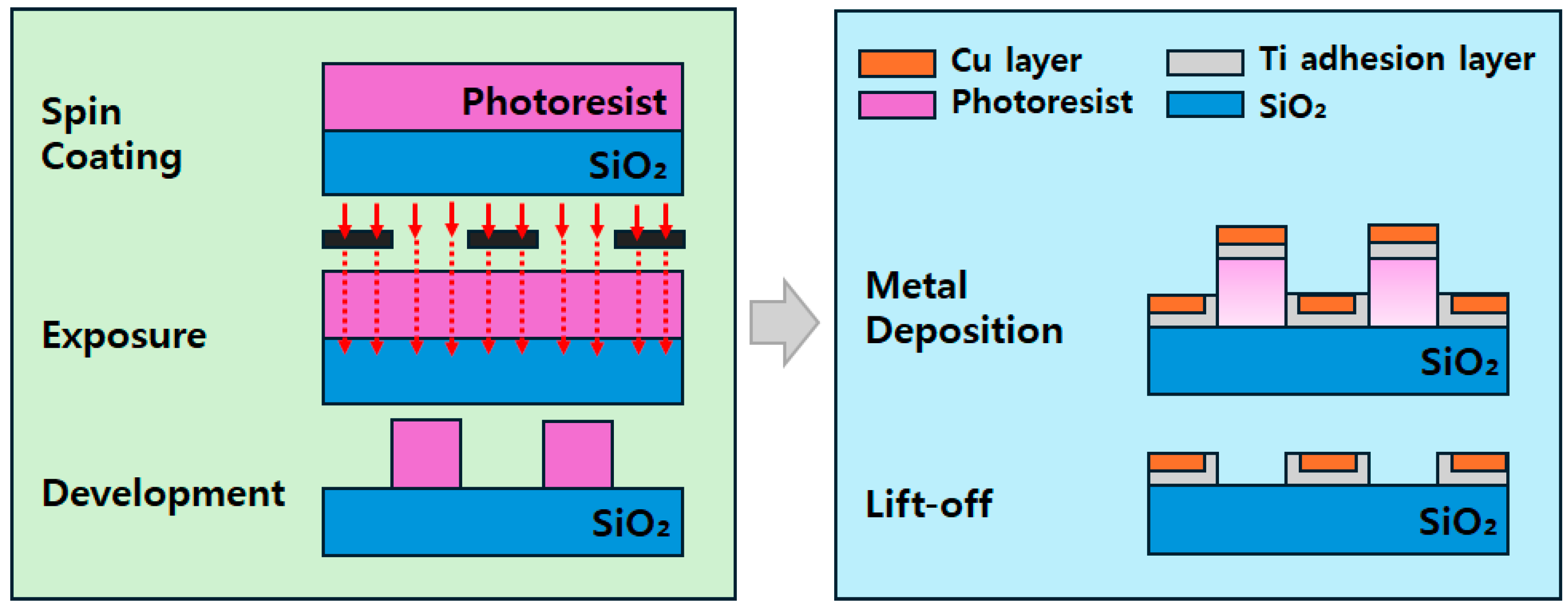
Figure 8 illustrates the overall process flow for forming metal interconnects on a substrate. The fabrication was conducted based on a lithography process, with key steps as follows: First, a photoresist layer was coated onto the substrate using spin coating, followed by exposure and development steps to form the desired pattern. Subsequently, metal deposition was performed to deposit a Ti adhesion layer and a Cu layer, and a lift-off process was carried out to finalize the interconnect structure. Through this process, samples with varying via lengths and contact areas were fabricated for experimental validation.
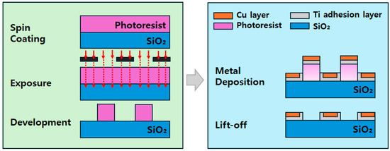
Figure 8.
Process flow for metal line formation on a SiO2 substrate.
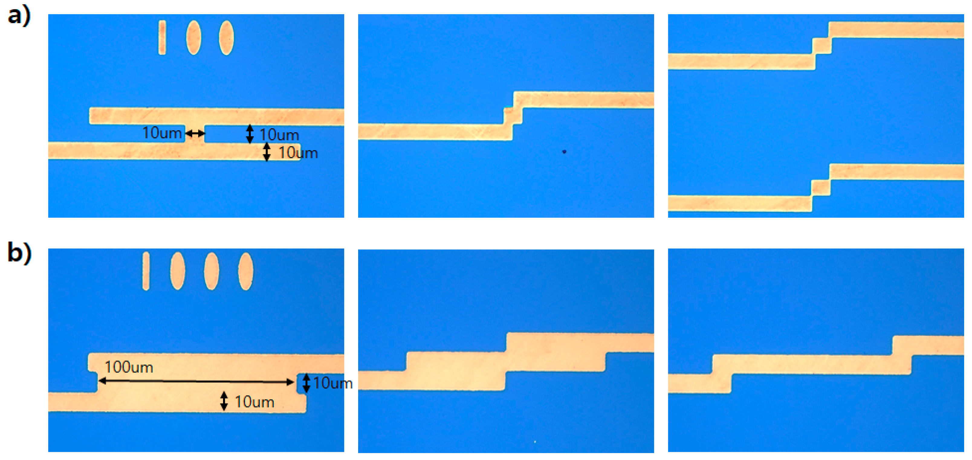
Figure 9a,b show an optical microscope (OM), MX61 microscope (Olympus Corporation, Tokyo, Japan), was used and images of structures with via lengths of 10 µm and 100 µm, respectively. Figure 9a presents three OM images, each corresponding to a via size of 10 µm, where the overlap area between the interconnect and via is 100% (over), 50%, and 10%, respectively. Similarly, Figure 9b displays three images in sequence for a via size of 100 µm, where the overlap area between the interconnect and via is 100% (over), 50%, and 10%, respectively. These images clearly depict the interconnect–via–interconnect structures, demonstrating that the contact area between the interconnect and via was progressively reduced as designed. This intentional misalignment was introduced to replicate the structures implemented in the simulation within the actual fabrication process.
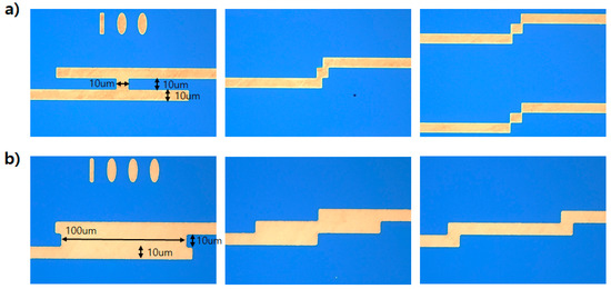
Figure 9.
Optical microscope (OM) images of the metal line–via–metal line structure with via lengths of (a) 10 μm and (b) 100 μm.
5. Results and Discussion
To analyze the impact of the contact area between the interconnect and via on resistance, various structures implemented in the simulation were fabricated through an actual process, and their resistance values were measured. Pads were formed at both ends of the interconnect, and resistance measurements were conducted using a probe station in a two-probe configuration. For electrical characterization, the MST4000 probe station (MSTECH, Gwangju, Republic of Korea) and the Keithley 4200 parameter analyzer (Keithley, Cleveland, OH, USA) were used, and the measurements were conducted under room temperature and atmospheric pressure conditions. The measurement conditions involved sweeping the voltage while recording the corresponding resistance values. The voltage sweep range was set from −0.5 V to 0.5 V, and resistance values for each structure were calculated using Ohm’s law (V = IR) based on the extracted voltage-current data [15]. To analyze how the measured resistance values vary with changes in the via–interconnect contact area, measurements were conducted on a total of eight different structures.
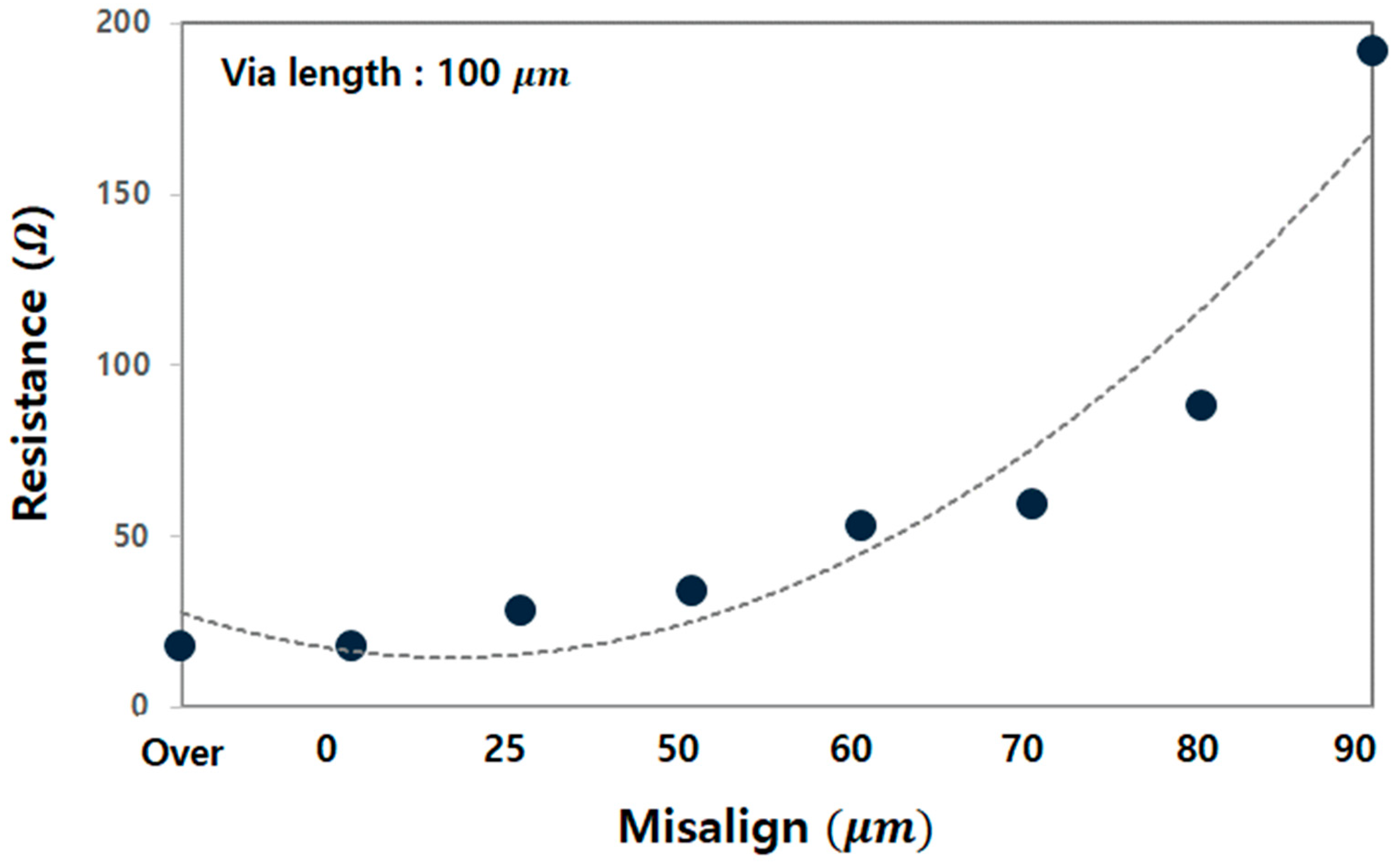
Figure 10 presents the resistance measurement results for the via structure with a length of 100 µm. The x-axis represents different structural configurations based on variations in the contact area. The label ‘Over’ indicates an excessive contact area, while ‘0’ represents a perfectly aligned via and interconnect. The subsequent labels, ‘25’, ‘50’, ‘60’, ‘70’, ‘80’, and ‘90’, denote structures where the contact length was progressively reduced to 25%, 50%, 60%, 70%, 80%, and 90% of the fully aligned state (0). The results indicate that resistance increases as the contact area decreases. Notably, beyond the ‘50’ mark, where only 50% of the via and interconnect are in contact, the resistance exhibits a sharp increase. This trend aligns with the predictions from the simulation, confirming that the simulation results are applicable to real fabrication processes.
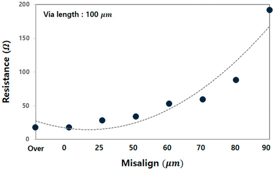
Figure 10.
Measured resistance values for the metal line-via-metal line structure with a via length of 100 µm as a function of misalignment.
‘Over’ indicates a state where the interconnect is fabricated larger than the via, extending beyond the via position, while ‘0’ represents a state where the ends of the via and interconnect are perfectly aligned. The values from 25 to 90 represent the degree of misalignment (20% to 90% misalignment). The results show that resistance increases as the contact area decreases, exhibiting an exponential trend. Notably, beyond the ‘50’ mark, where only 50% of the via and interconnect are in contact, the resistance increases sharply by more than 15%. This trend aligns with the predictions from the simulation, confirming that the simulation results are applicable to real fabrication processes. Therefore, even when an interconnect-to-via misalignment of up to 25% occurs, the actual increase in resistance is less than 10%, not proportional to the 25% misalignment. Utilizing these results, the margin allocated to account for interconnect-to-via misalignment can be reduced. In other words, it is possible to propose a design rule that allows for higher integration density by considering acceptable resistance loss limits.
This study experimentally verified that the current density and resistance characteristics of interconnect–via structures derived from simulations can be consistently applied to actual fabrication processes. Additionally, it demonstrated that optimizing design rule margins through process parameter adjustments can contribute to scaling down. These findings can serve as critical guidelines for margin allocation in future semiconductor interconnect design.
6. Conclusions
This study combined FEM simulations and actual fabrication processes to analyze the impact of unnecessary interconnect sections on current conduction in a metal line–via–metal line structure. Simulation results revealed that current density was primarily concentrated in approximately 20% of the interconnect height and along the diagonal edges of the via. Based on this, we hypothesized that optimizing the design of interconnects and via would allow for a reduction in unnecessary interconnect length without significantly affecting current conduction performance. To verify these simulation results, Si-based fabrication processes were conducted, designing various interconnect and via structures and measuring resistance values for comparison with simulation results. Experimental findings indicated that when the interconnect width was reduced below a certain threshold, resistance increased sharply due to process limitations. However, up to a certain point, interconnect width reduction had minimal impact on resistance, demonstrating the feasibility of more compact layouts. A comparison between simulation results and experimental data showed an agreement within an error range of 1–3%, confirming the reliability of the resistance calculation formula derived in this study.
This research suggests that optimizing interconnect and via structures can reduce unnecessary interconnect sections in integrated circuit design, thereby lowering fabrication costs and minimizing area usage. It also implies that a larger margin for misalignment in the patterning process during interconnect fabrication does not significantly impact current conduction. This finding can serve as a basis for establishing practical process limits in advanced semiconductor patterning, where extreme minimization of process constraints may not always be feasible. Additionally, it highlights the effectiveness of using FEM simulations for design optimization prior to experimental validation. Future studies should consider a wider range of process parameters to enhance the reliability of this approach and explore its applicability beyond silicon to other materials and fabrication technologies. By further refining design models for semiconductor process optimization and providing practical design guidelines, this research is expected to contribute to improving the efficiency of high-density semiconductor circuit design.
Author Contributions
Conceptualization, S.E.K. and S.K.H.; methodology, S.E.K. and S.K.H.; software, S.H.O. and T.Y.H.; validation, S.K.H.; formal analysis, S.H.O., T.Y.H., J.K.P. and S.K.H.; writing—original draft preparation, S.H.O.; writing—review and editing, J.K.P. and S.K.H.; visualization, S.H.O. and T.Y.H.; supervision, S.K.H.; project administration, S.K.H. All authors have read and agreed to the published version of the manuscript.
Funding
This work was supported by the National Research Foundation of Korea (NRF) grant funded by the Korean government (MSIT) (No. RS-2023-00239657 and No. RS-2024-00440244).
Institutional Review Board Statement
Not applicable.
Informed Consent Statement
Not applicable.
Data Availability Statement
The raw data supporting the conclusions of this article will be made available by the authors upon request.
Acknowledgments
The interconnect samples were fabricated using Sputtering System (SRN-110), Spin Coater, Aligner System, and Wet Station, S-FAB at Seoul National University of Science and Technology. The EDA tool was supported by the IC Design Education Center (IDEC), Korea.
Conflicts of Interest
The authors declare that they have no known competing financial interests or personal relationships that could have appeared to influence the work reported in this paper.
Abbreviations
| BEOL | Back end of line |
| FEM | Finite element method |
| FEOL | Front end of line |
| OM | Optical Microscope |
References
- Orlowski, M. CMOS Challenges of Keeping Up with Moore’s Law. In Proceedings of the 2005 13th International Conference on Advanced Thermal Processing of Semiconductors, Santa Barbara, CA, USA, 4–7 October 2005; p. 19. [Google Scholar] [CrossRef]
- Ye, Y. Advanced Packaging Trends in the Semiconductor Industry. Highlights Bus. Econ. Manag. 2024, 28, 8–12. [Google Scholar] [CrossRef]
- Chang, Y.W. Physical Design Challenges in Modern Heterogeneous Integration. In Proceedings of the 2024 International Symposium on Physical Design (ISPD ’24), Taipei, Taiwan, 12–15 March 2024; Association for Computing Machinery: New York, NY, USA, 2024; pp. 125–134. [Google Scholar] [CrossRef]
- Sharma, S.; Gupta, R.; Patel, A.; Kumar, V. Beyond Silicon: Emerging Materials and Technologies in Semiconductor Innovation. Int. J. Tech. Res. Sci. 2024, 9, 211. [Google Scholar] [CrossRef] [PubMed]
- Collaert, N. More Moore: From Device Scaling to 3D Integration and System-Technology Co-Optimization. In Proceedings of the 2017 Silicon Nanoelectronics Workshop (SNW), Kyoto, Japan, 4–5 June 2017; pp. 123–124. [Google Scholar] [CrossRef]
- Chakravarti, J.; Panchal, C. Test Time Reduction with Data Throttling Techniques in a Multi-Core SoC Design. In Proceedings of the 2024 28th International Symposium on VLSI Design and Test (VDAT), Vellore, India, 1–3 September 2024; pp. 1–4. [Google Scholar] [CrossRef]
- Joshi, A.; Sethi, R.; Kumawat, P. Review of Electromagnetic Failure, Optimization Techniques and Stress Prediction in Interconnect. IOSR J. VLSI Signal Process. 2014, 4, 23–28. [Google Scholar]
- Darewar, T.P.; Dighe, D.D. Enhancement in Power-Delay Product by Driver and Interconnect Optimization. Int. J. Res. Eng. Technol. 2014, 3, 411–417. Available online: https://engg.matoshri.edu.in/assets/pdf/electronics/achievements/1DDD/published/32.%20Enhancementinpower-delayproductbydriverandinterconnectoptimization-140820041537-phpapp01.pdf (accessed on 6 February 2025).
- Huang, P. Design and Optimization of CMOS Layout Structure for Improved Semiconductor Device Performance. J. Phys. Conf. Ser. 2023, 2649, 012034. [Google Scholar] [CrossRef]
- Calhoun, B.H.; Chandrakasan, A.P.; Winstead, C.; Zhang, Z. Digital Circuit Design Challenges and Opportunities in the Era of Nanoscale CMOS. Proc. IEEE 2008, 96, 343–365. [Google Scholar] [CrossRef]
- Yang, J.S.; Athikulwongse, K.; Lee, Y.J.; Lim, S.K.; Pan, D.Z. TSV Stress Aware Timing Analysis with Applications to 3D-IC Layout Optimization. In Proceedings of the 47th Design Automation Conference (DAC ’10), Anaheim, CA, USA, 13–18 June 2010; Association for Computing Machinery: New York, NY, USA, 2010; pp. 803–806. [Google Scholar] [CrossRef]
- Hong, T.Y.; Kim, S.E.; Park, J.K.; Hong, S.K. Analysis of Signal Transmission Efficiency in Semiconductor Interconnect and Proposal of Enhanced Structures. Micromachines 2024, 15, 1207. [Google Scholar] [CrossRef] [PubMed]
- He, F.; Tan, C.M. Circuit Level Interconnect Reliability Study Using 3D Circuit Model. Microelectron. Reliab. 2010, 50, 376–390. [Google Scholar] [CrossRef]
- Weide, K.; Hasse, W. 3-Dimensional Simulations of Temperature and Current Density Distribution in a Via Structure. In Proceedings of the 30th Annual Reliability Physics Symposium, San Diego, CA, USA, 31 March–1 April 1992; pp. 361–365. [Google Scholar] [CrossRef]
- Tenny, K.M.; Keenaghan, M. Ohm’s Law. In StatPearls; StatPearls Publishing: Treasure Island, FL, USA, 2023. [Google Scholar] [PubMed]

Disclaimer/Publisher’s Note: The statements, opinions and data contained in all publications are solely those of the individual author(s) and contributor(s) and not of MDPI and/or the editor(s). MDPI and/or the editor(s) disclaim responsibility for any injury to people or property resulting from any ideas, methods, instructions or products referred to in the content. |
© 2025 by the authors. Licensee MDPI, Basel, Switzerland. This article is an open access article distributed under the terms and conditions of the Creative Commons Attribution (CC BY) license (https://creativecommons.org/licenses/by/4.0/).