1. Introduction
Sinusoidal oscillators play an essential role in most electronic systems. They find numerous applications in instrumentation, measurement, control and communication systems. New oscillator circuits based on various active elements have been proposed continuously [
1,
2,
3,
4]. Most oscillators proposed in the literature have been on an
ad hoc basis,
i.e., a topology is chosen using an arbitrary procedure and is then analyzed. For the design of oscillator circuits, it is useful to follow systematic methodologies to obtain novel circuits. This is beneficial in developing analog tools for circuit design automation. The first systematic synthesis of canonic oscillators using controlled sources was given in [
5]. The design of single op-amp single resistance controlled oscillators was reported in [
6]. The generation method by using unity gain cells was given in [
7]. Generalized synthesis approach for Gm-C oscillators using the signal flow graph approach was given in [
8,
9]. A systematic state-variable approach to the synthesis of canonic current feedback op-amps-based oscillators was given in [
10]. In recent times, the concepts of pathological elements have been proven to be very useful for circuit analysis, transformation and synthesis. Their applications have been presented in the literature [
11,
12,
13,
14]. By the use of nodal admittance matrix expansion method and pathological elements, the systematic synthesis of the current conveyor-based active RC canonic oscillators was reported in [
15,
16].
To conveniently derive oscillator circuits, a systematic synthesis method is presented in this paper. By exploiting circuit transformations to the original biquadratic band pass filter, the oscillator circuit can be obtained. It retains some useful properties of the original band pass filter. Two circuit examples are given to demonstrate the feasibility of the proposed method. The workability of the derived oscillators is verified by PSPICE simulation.
2. Description of the Proposed Method
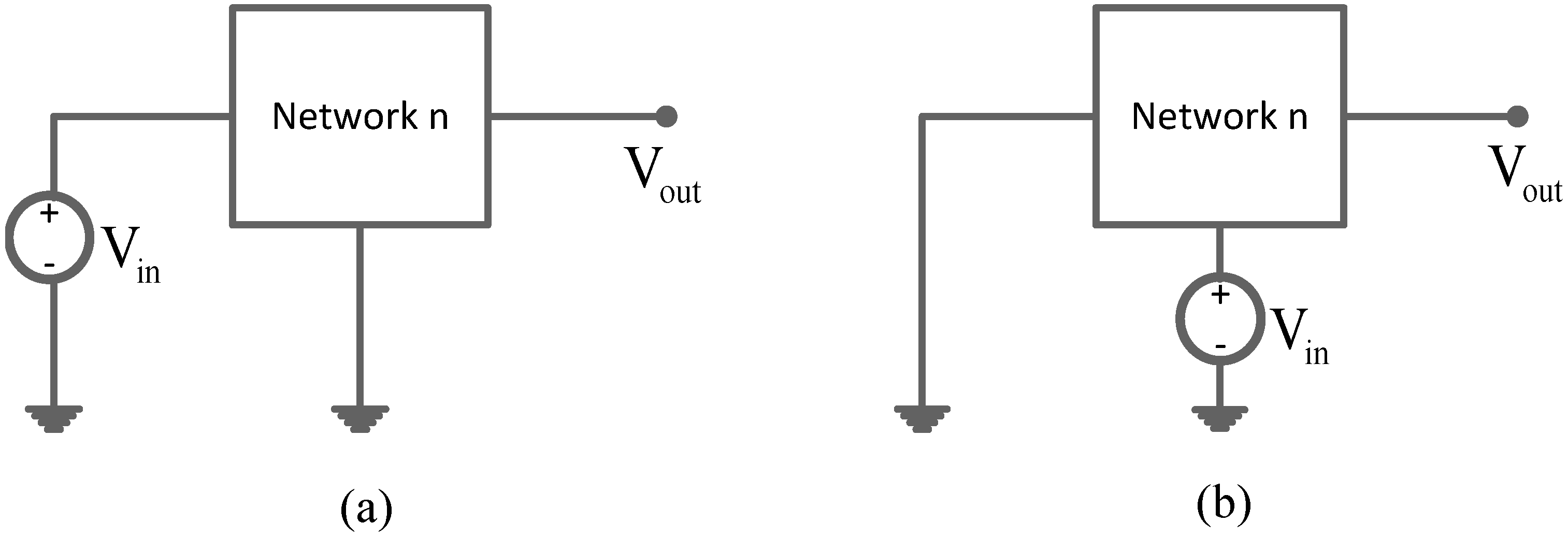
The proposed approach involves the use of complementary and inverse transformations. One can obtain a complementary voltage-mode network by interchanging the input and ground of a circuit [
17,
18], as shown in
Figure 1. The resulting transfer function (TRANSF) T
2 of the obtained circuit would be the complement (COMP) of the original voltage transfer function T
1;
i.e., T
2 = 1 − T
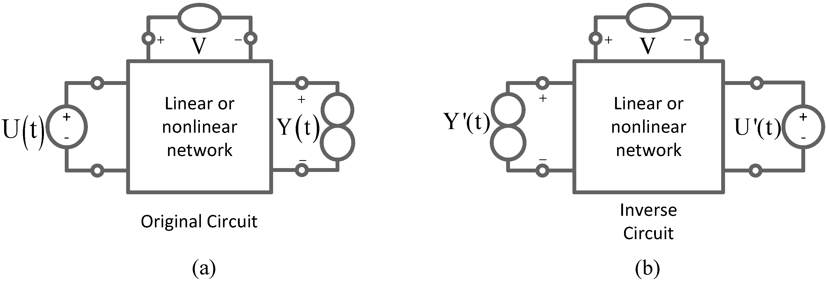
1. According to inverse transformation by interchanging the output norator and the input voltage source of a circuit (with its transfer function T
3 = Y/U), the inverse transfer function (INV) can be obtained as T
3' = 1/T
3 = Y'/U'), as shown in
Figure 2 [
12]. The inverse network can also be obtained by interchanging the output pathological current mirror and the input source of a circuit [
19]. To obtain a sinusoidal oscillator from the biquadratic band pass filter, the combination of circuit transformations can be exploited, as the stages shown in
Table 1 and
Table 2.
Figure 1.
The complementary transformation for voltage-mode a network. (a) Original network; (b) complementary network of (a).
Figure 1.
The complementary transformation for voltage-mode a network. (a) Original network; (b) complementary network of (a).
Figure 2.
The inverse transformation of a circuit. (a) Original network; (b) inverse network of (a).
Figure 2.
The inverse transformation of a circuit. (a) Original network; (b) inverse network of (a).
Table 1.
The combination of complementary-inverse transformation (TRANSF) for a voltage-mode network. COMP, complement; INV, inverse transfer function.
Table 1.
The combination of complementary-inverse transformation (TRANSF) for a voltage-mode network. COMP, complement; INV, inverse transfer function.
| Procedure | Stage (0) | Stage (1): | Stage (2): | Stage (3): |
|---|
| COMP of (0) | INV of (1) | COMP of (2) |
|---|
| TRANSF | T | 1-T | | |
Table 2.
Another combination of complementary-inverse transformation for a voltage-mode network.
Table 2.
Another combination of complementary-inverse transformation for a voltage-mode network.
| Procedure | Stage (0) | Stage (1): | Stage (2): | Stage (3): |
|---|
| INV of (0) | COMP of (1) | INV of (2) |
|---|
| TRANSF | T | 1/T | | |
To describe the synthesis method clearly, a biquadratic voltage-mode band pass filter with its transfer function given by Equation (1) is considered. The pole frequency ω
o and bandwidth (BW) of the filter can be computed as ω
o =
and BW = ω
o/Q =
b, where Q is the quality factor of the filter. The coefficient
b and
c are always greater than zero for a stable system.
Applying the proposed procedure in
Table 1 or
Table 2 to this filter, we obtain its new transfer function as Equation (2).
Namely, the new filter with ω
o =
and ω
o/Q = (
b −
a) is derived.
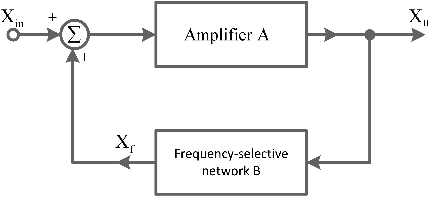
For a positive-feedback system in
Figure 3 with a stable amplifier stage
A(
s) and a frequency-selective network
B(
s) connected in a positive-feedback loop, the closed-loop gain
Af(
s) can be expressed by:
If at a specific pole frequency ω
o the loop gain
A(
s)
B(
s) is equal to unity,
Af will be infinite. That is, at this frequency, the system defined as an oscillator will have a finite output for zero input signal. Thus, the condition for the feedback loop of
Figure 3 to provide sinusoidal oscillations of frequency ω
o is:
This is known as the Barkhausen criterion. Therefore, a linear oscillator can be synthesized by zeroing the input source of the filter [
18]. The obtained characteristic equation of the oscillator can be expressed as Equation (5). The oscillation condition is given by Equation (6) and oscillation frequency can be expressed by ω
o =
.
In general, Equation (6) can be easily satisfied by selecting suitable passive components of the original band pass filter.
Figure 3.
A positive-feedback system with a stable amplifier stage, A, and a frequency-selective network, B.
Figure 3.
A positive-feedback system with a stable amplifier stage, A, and a frequency-selective network, B.
It is known that the grounded nullator and norator will be conductive to lower active sensitivities of a circuit [
20]. The proposed oscillator synthesis procedure includes performing inverse transformation and zeroing the input signal source. This will result in the circuit processes grounded nullator and norator (as we add a series nullator-norator pair between the outputted node and the ground and then interchange the inputted signal source with outputted norator to perform inverse transformation). Therefore, an oscillator with lower active sensitivities may be derived. Therefore, the obtained oscillator has identical passive sensitivities and may have improved active sensitivities with respect to the original band pass filter.
3. Application Examples and Discussion
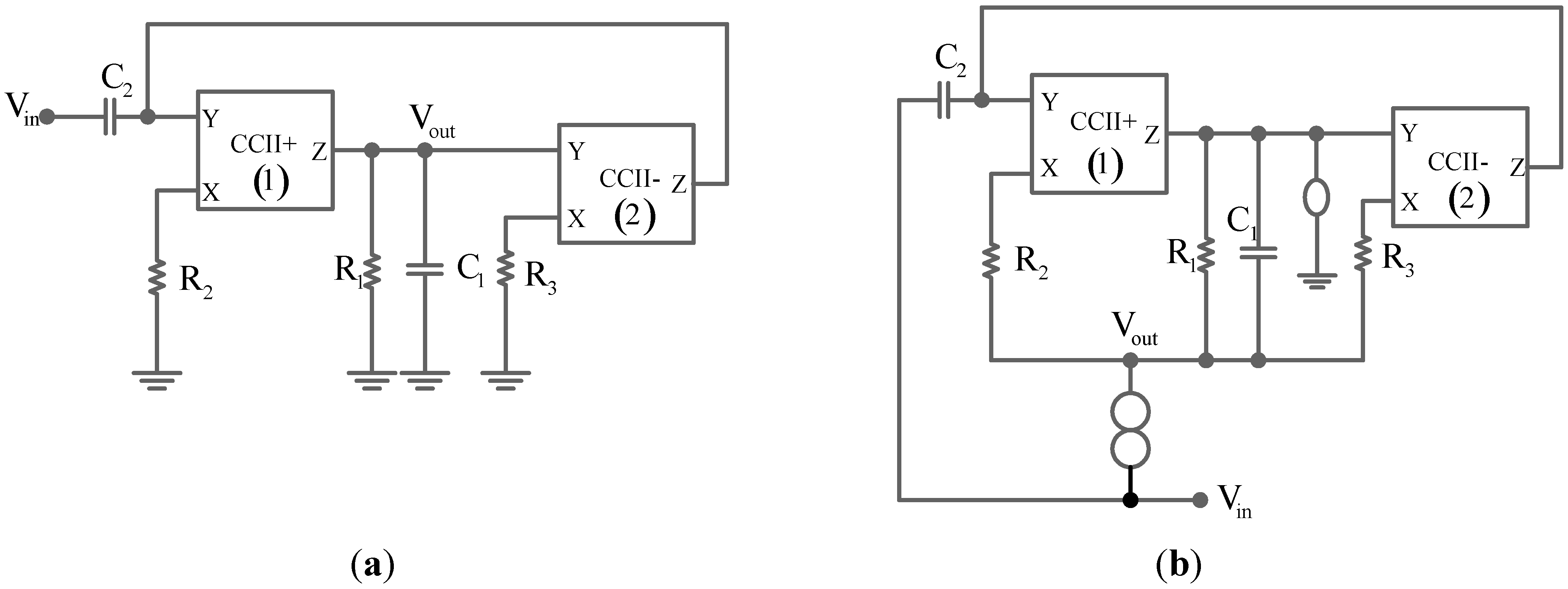
To demonstrate the feasibility of the proposed method, we first consider the voltage-mode low active and passive sensitivities band pass filter modified from the filter circuit in
Figure 1 of [
21], as redrawn in
Figure 4a. Its transfer function is given by Equation (7). By using the transformation in
Table 1, the obtained circuit with its transfer function given by Equation (8) is shown in
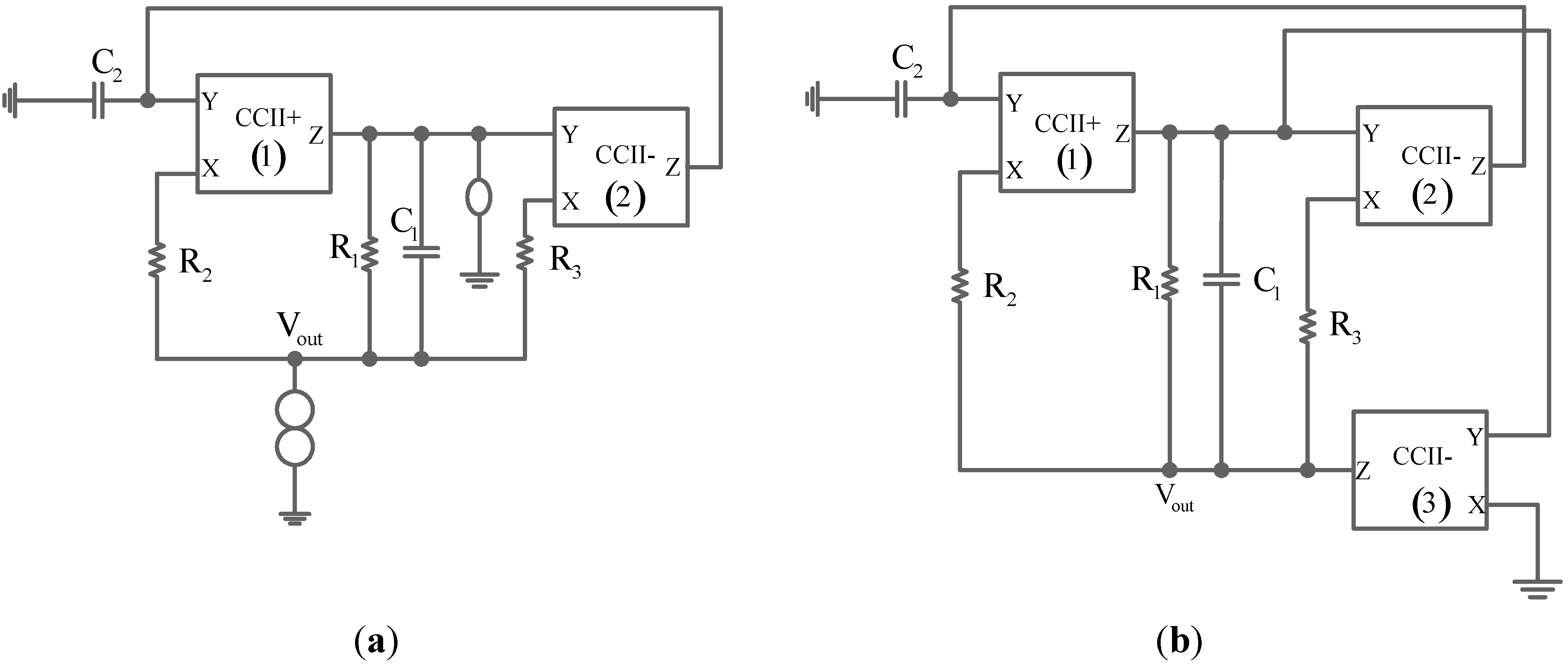
Figure 4b. A series nullator-norator pair is added during performing the inverse transformation. By zeroing the input signal source, we obtain the oscillator in
Figure 5a. The nullator-norator pair in
Figure 5a can be realized by a second generation current conveyor (CCII-) [
16], as shown in
Figure 5b. Taking into account the non-idealities of a current conveyor, namely I
Z = ±αI
X, V
X = βV
Y, where α = 1 − e
i and e
i denotes the current tracking error, β = 1 − e
v and e
v denotes the voltage tracking error of a current conveyor, respectively, the non-ideal characteristic equation of the oscillator is expressed by Equation (9). Its oscillation condition and oscillation frequency ω
o are given by Equations (10) and (11), respectively. The sensitivities of ω
o to active and passive components are given in Equation (12). It is clear that the obtained oscillator has identical passive sensitivities and has improved active sensitivities compared to the original band pass filter [
21]. In addition, the oscillation frequency and the oscillation condition are independently adjustable through with
R3 and
R1. In reality,
R1 must be slightly greater than
R2/α
1 for the startup of oscillation [
22].
Figure 4.
(
a) A CCII-based band pass filter; (
b) the obtained filter after applying the transformations in
Table 1.
Figure 4.
(
a) A CCII-based band pass filter; (
b) the obtained filter after applying the transformations in
Table 1.
Figure 5.
(a) The obtained oscillator; (b) realization of the obtained oscillator in (a).
Figure 5.
(a) The obtained oscillator; (b) realization of the obtained oscillator in (a).
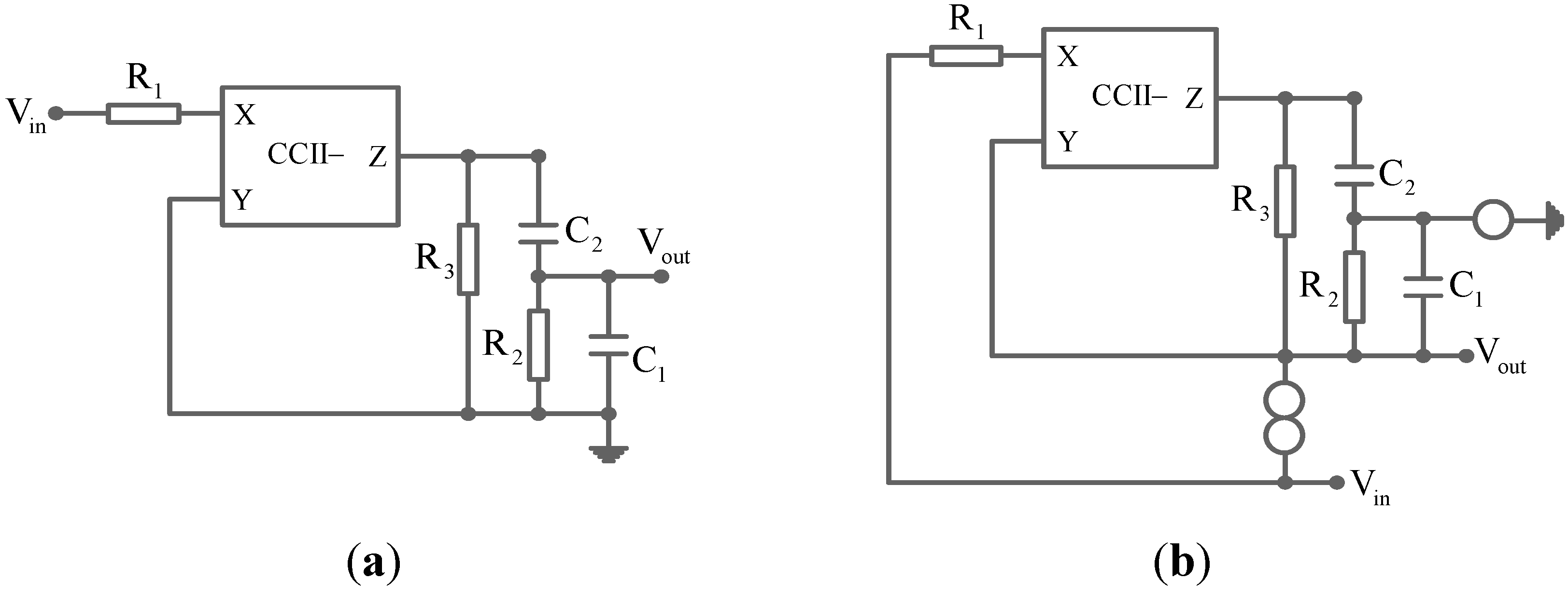
The second example considers the single CCII-based voltage-mode band pass filter, which is obtained from [
23], as shown in
Figure 6a. Using the transformed procedure mentioned in
Table 2, the derived circuit with its transfer function shown in Equation (13) is given by
Figure 6b.
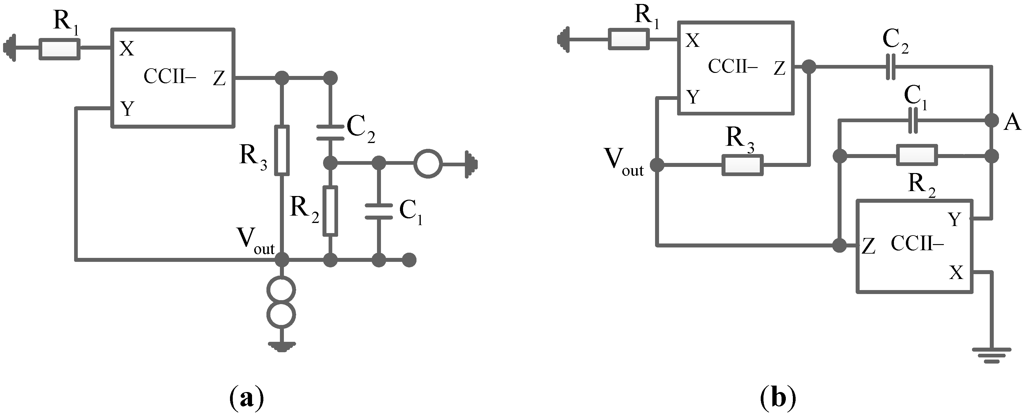
Figure 7a shows the derived oscillator by grounding the input source of the circuit in
Figure 6b. The nullator and norator in
Figure 7a can be realized by a CCII-, as shown in
Figure 7b. The characteristic equation of the obtained oscillator can be expressed by Equation (14). The oscillation condition and the oscillation frequency can be respectively given by Equations (15) and (16) with
R2 =
R3 =
R and
C1 =
C2 =
C. It can be found that the oscillation condition and oscillation frequency are orthogonal adjustable. It must be noted that
R1 must be slightly less than
R/3 for the startup of oscillation.
Figure 6.
(
a) A CCII-based band pass filter; (
b) the obtained filter after applying the transformations in
Table 2.
Figure 6.
(
a) A CCII-based band pass filter; (
b) the obtained filter after applying the transformations in
Table 2.
Figure 7.
(
a) Grounding input of
Figure 6b; (
b) realization of the obtained oscillator in (
a).
Figure 7.
(
a) Grounding input of
Figure 6b; (
b) realization of the obtained oscillator in (
a).
Moreover, it can be found that the oscillator in
Figure 7b possesses an electrically controllable function of the oscillation condition by using a controlled current conveyor (CCCII-) to realize the CCII- and
R1. It is known that the ground node of a nullor-based oscillator can be chosen arbitrarily without affecting the characteristic equation [
24]. Therefore, the grounded capacitor oscillator can be obtained by selecting Node A in
Figure 7b as the ground. In addition, more oscillators can be obtained by applying adjoint network theorem or RC-CR transformation.
It must be noted that the proposed method can be applied to any band pass filters, so it has better generality compared to the transformed method in [
25], which can only be applied to the filters with specific configuration and cascadable property. Furthermore, since the oscillation frequency of the synthesized oscillator is identical to the center frequency of the original band pass filter, one can obtain high-performance oscillators by choosing the suitable band pass filters for transformation. For example, the aforementioned band pass filters with low-sensitivity or electronically adjustability can be selected to obtain useful oscillators. Furthermore, current-mode linear oscillators can also be derived according to the proposed method, because the complementary and inverse transformations can be applied to current-mode circuits.
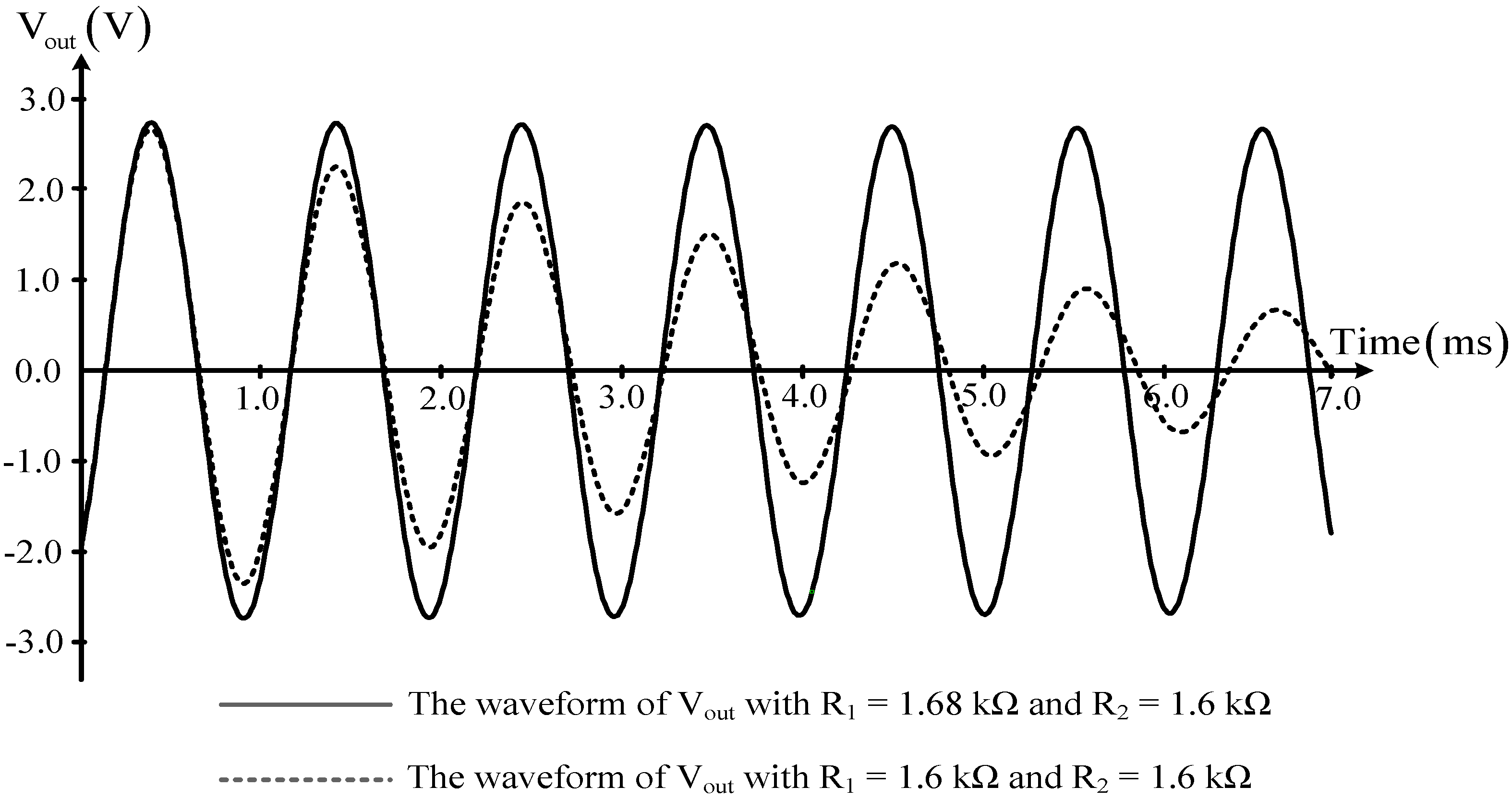
4. Simulation Results
To verify the theoretical prediction of the proposed method, PSPICE simulations were performed for the obtained linear oscillators in
Figure 5b and
Figure 7b. The CCII+ and CCII- were realized by current feedback operational amplifier (AD844) ICs [
26,
27]. The macromodels of AD844 were employed for the simulations with a DC supply of ±15 V. For the circuit in
Figure 5b, we chose
C1 =
C2 =
C = 0.1 µF and
R2 =
R3 = 1.6 kΩ. As shown in
Figure 8, the oscillation eventually died out with
R1 = 1.6 kΩ, and the circuit produced a pure sinusoidal waveform with
R1 = 1.68 kΩ.
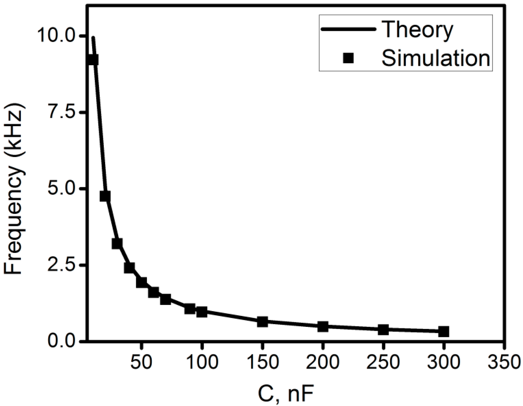
Figure 9 shows the oscillation frequency for various values of
C. It confirms the independently tunability of the oscillation frequency. For the oscillator in
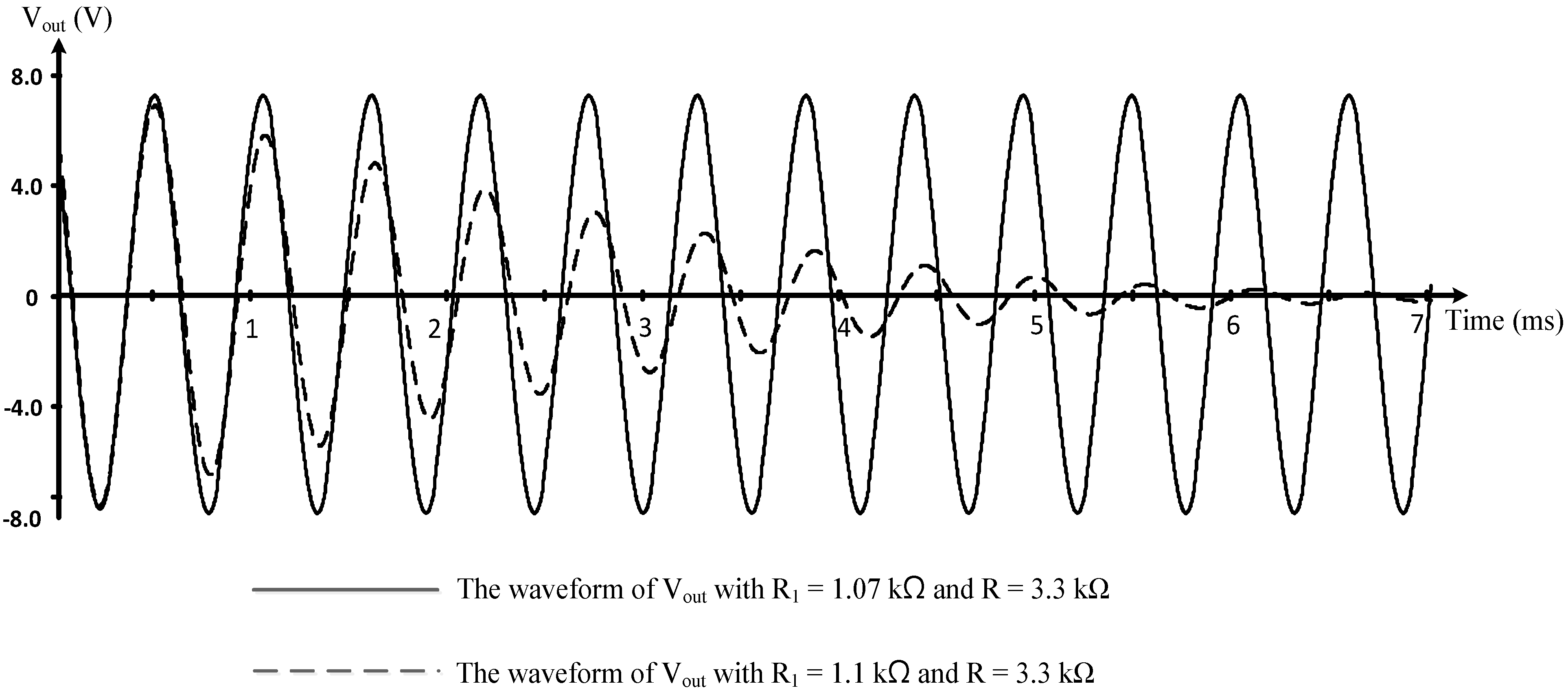
Figure 7b, we choose
C1 =
C2 = 27 nF and
R2 =
R3 = 3.3 kΩ.
Figure 10 shows the outputted waveforms with
R1 = 1.07 kΩ and
R1 = 1.1 kΩ. All if the simulation results are consistent with our prediction in
Section 3.
Figure 8.
The output waveforms for the oscillator in
Figure 4b with different oscillation conditions.
Figure 8.
The output waveforms for the oscillator in
Figure 4b with different oscillation conditions.
Figure 9.
Theoretical and simulation results, varying values of C.
Figure 9.
Theoretical and simulation results, varying values of C.
Figure 10.
The output waveforms for the oscillator in
Figure 6 with different oscillation conditions.
Figure 10.
The output waveforms for the oscillator in
Figure 6 with different oscillation conditions.


