1. Introduction
Recently, high-efficiency GaN-based light-emitting diodes (LEDs) have been used in a wide range of applications, such as full-color displays, traffic signals, automobiles, solid-state lighting, and backlights of liquid-crystal displays [
1,
2,
3]. To achieve the high output power, the chip size of a LED device is typically enlarged for sustaining the high-injection-current operation. However, when a high injection current is applied in the device operation, the problem of LED efficiency droop occurs frequently because carrier overflow forms in the quantum wells [
4,
5].
To solve this problem, the high-voltage LEDs (HV-LEDs) were proposed. The HV-LED is defined as a GaN-based LED with series-connection micro-cells, which can be operated at a voltage higher than 20 V and an injection current lower than 100 mA [
6,
7,
8,
9,
10,
11,
12]. The design and fabrication of HV-LEDs can eliminate the problem of efficiency droop and maintain the high output power. In addition to reducing efficiency droop, applying HV-LEDs can improve the current spreading. When the HV-LEDs are used, the injection current spreads uniformly to all micro-cell LEDs and turns on all chips. This phenomenon can enhance the output power of LEDs. For example, the total output power of HV-LEDs is double that of alternating current LEDs (AC-LEDs) that have a configuration similar to that of HV-LEDs and the same injection current. This doubled output power can be attributed that only half of the active area is driven when an AC-LED is operated.
In recent studies, HV-LEDs have exhibited superior performance in reducing efficiency droop and an improved output power compared with conventional LEDs and AC-LEDs. However, these studies focused on the lateral LEDs fabricated on sapphire substrates. For lateral LEDs, the current-crowding phenomenon and low heat-conducting problem caused by the poor electrical and thermal conductivities of sapphire substrates inhibit the device performance. Additionally, the waveguide effect is unavoidable in the sapphire-based LED structure and reduces light intensity because of the limitation of the light path.
At present, several techniques consisting of flip-chip packaging [
12] and vertical-type structure [
13] were proposed to overcome the disadvantage of low heat dissipation occurred in the lateral LEDs. In this study, vertical HV-LEDs were proposed to further enhance the device performance. The metal bonding process and laser lift-off technique were both employed to transfer HV-LEDs from sapphire to Cu metal substrates featuring a high thermal conductivity, resulting in the improved heat dissipation in the LEDs. In addition, the drawback of the waveguide effect in lateral LED structures can be solved efficiently by using vertical LEDs, thus improving the light emission efficiency. Moreover, the micro-cell geometry of the HV-LEDs was also modified to enhance the optoelectronic performance.
2. Experimental Procedures
In this study, the epitaxial structures of blue LEDs with an emission wavelength of 450 nm were prepared on c-plane (0001) sapphire substrates (Wafer Works Corporation, Taoyuan, Taiwan) by metalorganic chemical vapor deposition. The epilayers included a Si-doped n-type GaN layer (3 μm), ten pairs of InGaN/GaN MQWs with a 3-nm-thick un-doped well and a 12-nm-thick n-doped barrier as active regions, and the Mg-doped p-type GaN layer (150 nm). For the device process, the Ni/Ag/Ni/Pt (15/500/50/80 nm) metal multilayer deposited by e-beam evaporation on the p-type GaN was used as the contact layer. The Ni/Ag layer acted as both an Ohmic contact layer and a reflective mirror layer. The reflectivity of the mirror was measured to be 92% at 450 nm. Additionally, after the sample was annealed at 550 °C in N2 ambient for 3 min, a specific contact resistance as low as 5 × 10⁻⁵ Ω-cm2 can be obtained. To enhance the light extraction, a NaOH solution (4M) was employed to roughen the surface of the n-type GaN layer at 80 °C for 6 min. The LED device was fabricated using standard photolithography and etching processes in sequence.
To prepare the vertical HV-LED, the wafer bonding and laser lift-off techniques were applied as follows. For the wafer bonding process, In/Au and Au layers were grown on a metal substrate and LED sample, respectively, and then diffusion-bonded to each other at 200 °C. A laser lift-off process was used immediately to detach the sapphire substrate and LED sample. At this stage, the LED sample was successfully transferred to a Cu metal substrate.
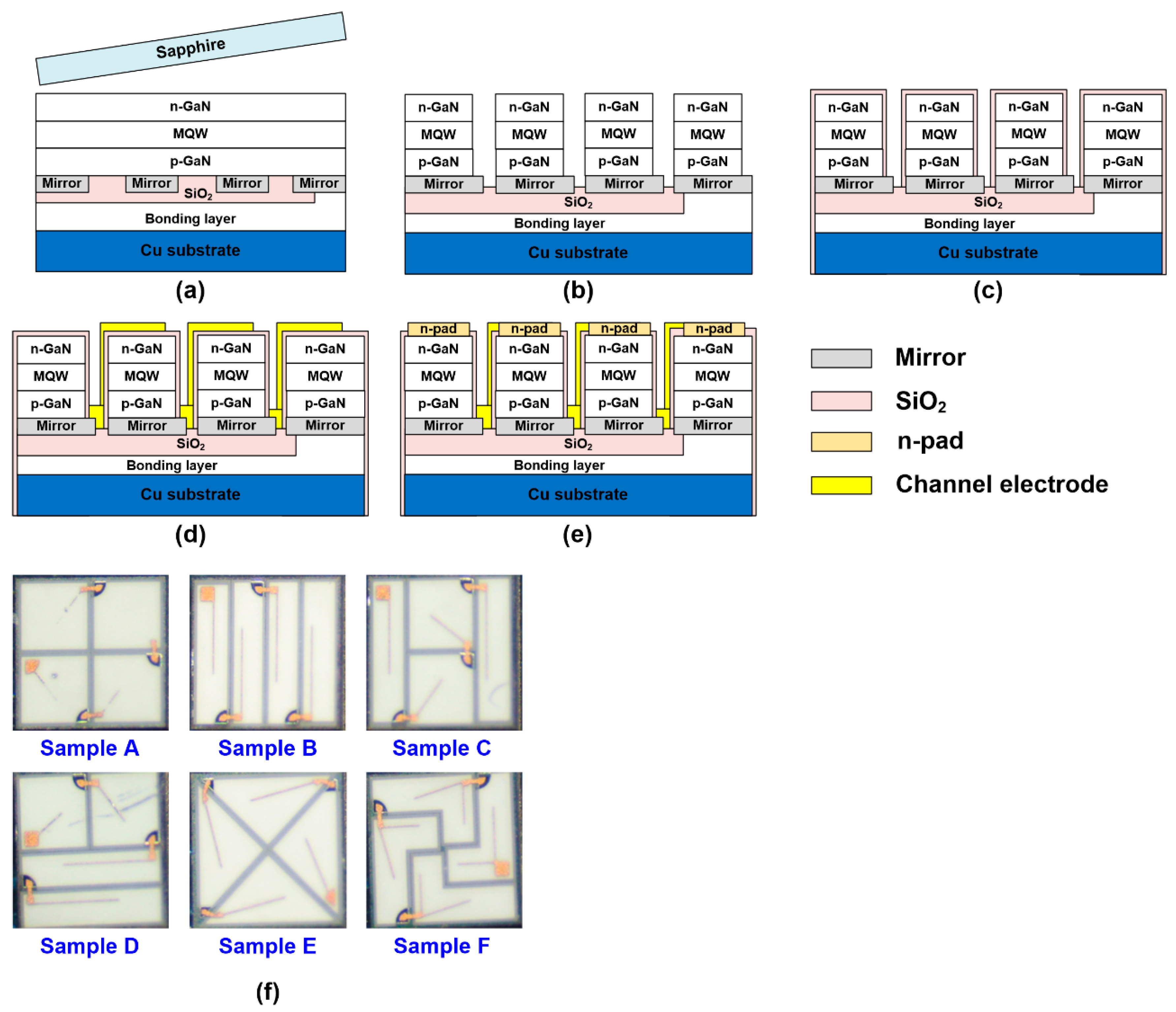
Figure 1a displays a diagram of this device (single cell). Next, the HV-LED was constructed in a 2 × 2 micro-cell LED configuration. The mesa pattern of each micro-cell LED was subsequently defined as having a size of 1016 × 1016 µm (
Figure 1b). Moreover, as shown in
Figure 1c, a SiO
2 layer was used as the passivation layer for the flatness of trenches between cell chips. The 2 × 2 cell LED array was connected using a Ti/Al/Ti/Au (20/1500/20/200 nm) channel electrode (
Figure 1d). Finally, the Cr/Au (20 nm/200 nm) was grown by thermal evaporation to form the n-pad electrode (
Figure 1e). Meanwhile, the Cu metal substrate plays the role of a p-pad electrode. To improve the optoelectronic performance of vertical HV-LEDs, the geometry of micro-cell was modified.
Figure 1f shows the images of the HV-LEDs with various cell shapes and chip arrangements before operating, denoted as Samples A–F, respectively. Several micro-cell geometries consisting of square, rectangle, triangle, and L shapes were designed. In Samples A–E, a single-line electrode was prepared on a single cell. However, Sample F was fabricated by combining four L-shaped cell chips. To enhance the current spreading effect of the L-shaped cell, a two-line electrode was formed on the single cell.
The current–voltage (I–V) characteristic of the device was measured by a semiconductor parameter analyzer (Keithley 2400 Sourcemeter, Keithley Instruments, Cleveland, OH, USA), and the output power was analyzed using a calibrated integrating sphere. The surface morphology of the roughened n-type GaN layer was observed by scanning electron microscopy (SEM) (S-3000H, Hitachi, Tokyo, Japan). The spatial distribution image of the light output for the HV-LED was obtained using a near-field optical microscope (Beamstar FX-50, Ophir-Spiricon, North Logan, UT, USA) combined with a charge-coupled device. The temperature distribution of the HV-LED sample surface was determined using thermal infrared imaging under a sealed atmosphere at room temperature. To obtain reliable data, these images were taken after a sufficiently long waiting time to reach the thermal steady state.
3. Results and Discussion
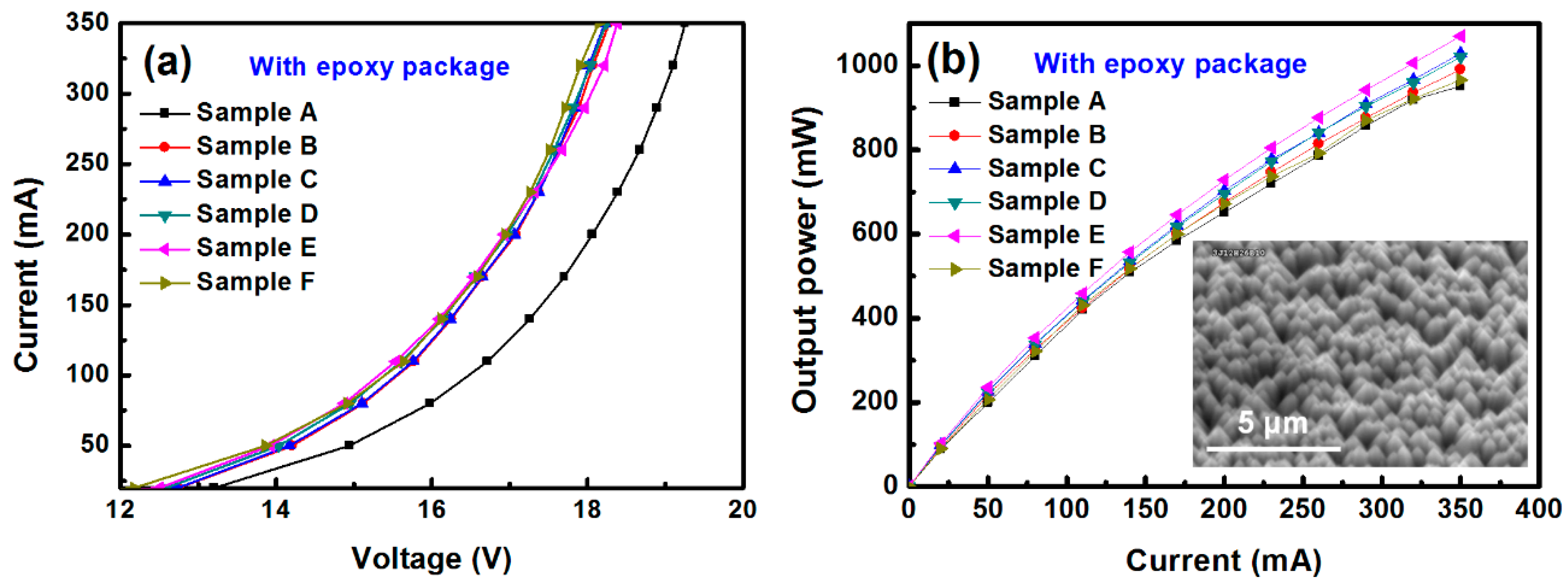
Figure 2a shows the I–V characteristics of the HV-LEDs (Samples A–F) after performing the epoxy package process. The injection current was increased from 20 to 350 mA. At injection currents of 20 and 80 mA, the forward voltages of Samples A–F were 13.2 and 16.0 V, 12.7 and 15.1 V, 12.7 and 15.1 V, 12.6 and 15.0 V, 12.5 and 14.9 V, and 12.2 and 14.9 V, respectively. When the injection current was increased to 350 mA, the forward voltages of these six HV-LEDs increased to 19.3, 18.3, 18.2, 18.2, 18.4, and 18.1 V, respectively. The I–V characteristics of Samples B–F were similar to each other. It indicates that our fabrication processes for vertical HV-LEDs are highly stable. However, the forward voltage of Sample A was clearly higher than that of the other HV-LEDs. Except for the I–V characteristics, the light output powers for the epoxy-packaged HV-LEDs were also measured.
Figure 2b shows the light output powers as a function of injection current from 0 to 350 mA for packaged Samples A–F. The surface morphology of the roughened n-type GaN layer taken by SEM is shown in the inset of
Figure 2b. For Samples A–F, the output powers at 20 and 80 mA were 89.2 and 309.9 mW, 91.7 and 326.9 mW, 98.4 and 339.7 mW, 96.6 and 338.1 mW, 102.8 and 353.2 mW, and 90.6 and 321.5 mW, respectively. At an injection current of 350 mA, the output powers of these six HV-LEDs increased to 951.2, 991.1, 1029.3, 1021.1, 1070.2, and 966.2 mW, respectively. Obviously, Sample E possessed the optimal light emission performance. Moreover, when the injection current was increased from 20 to 350 mA, the lowest output powers almost occurred in Sample A.
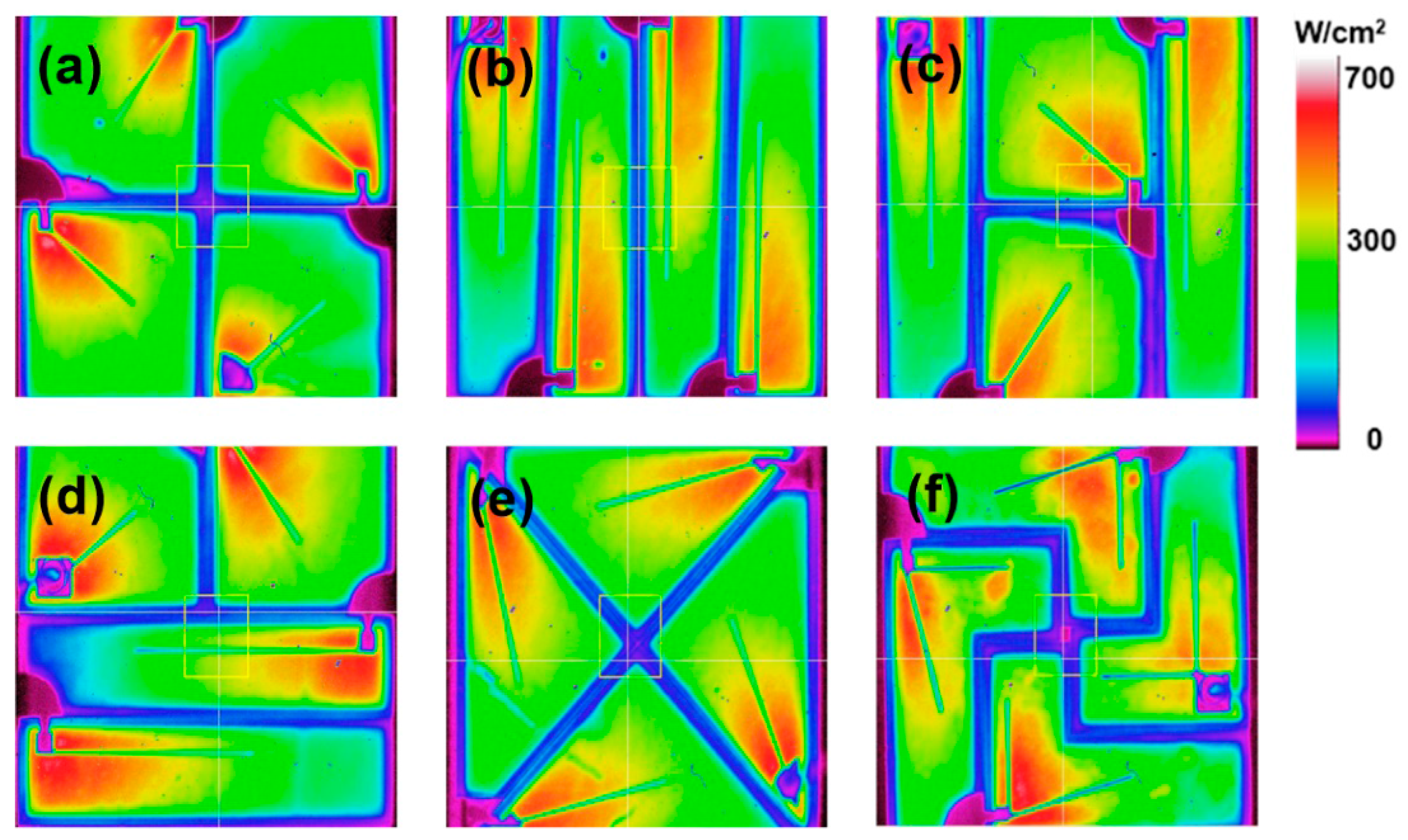
The spatial distribution images of the light output for Samples A–F are presented in
Figure 3a–f, respectively, at an injection current of 20 mA. In these images, the red/yellow and green/blue colors indicate high and low brightness, respectively. As shown in these images, the performances of light emission were similar to each other. On the other hand, we observed that some obstructions to the emitted light all appeared in these six samples, which resulted from the electrodes. The obstruction of the emitted light near the electrodes was much more obvious in Sample A, likely resulting from the current-crowding phenomenon. In addition, Samples B–F had a favorable current spreading effect. Especially for Samples B, E, and F, the emitted lights of these three samples were more uniform than that of the other HV-LEDs. Actually, the current spreading in micro-cell is most dominantly affected by the distance between electrode and edge of chip. Thus, the shape of micro-cell has no significant influence on the current spreading behavior. On the contrary, the charge diffusion length between electrode and edge of micro-cell plays a more important role than the cell shape for the current spreading behavior. When the electrodes were close to the edges of micro-cells, the current spreading effect can be easily enhanced, as shown in Samples B, E, and F. However, in Sample A, the electrodes in these four micro-cells were all far away from the edges, leading to its severe current-crowding phenomenon. Moreover, the current densities of these six samples were also analyzed via the calculations (i.e., injection current divided by actual emission area). For Samples A–F, the current densities (@20 mA) were determined to be 9.86, 10.84, 10.41, 10.35, 10.71, and 10.77 A/cm
2, respectively. The result agrees well with the effect of the charge diffusion length between the electrode and edge on the current spreading behavior of these samples that we have described.
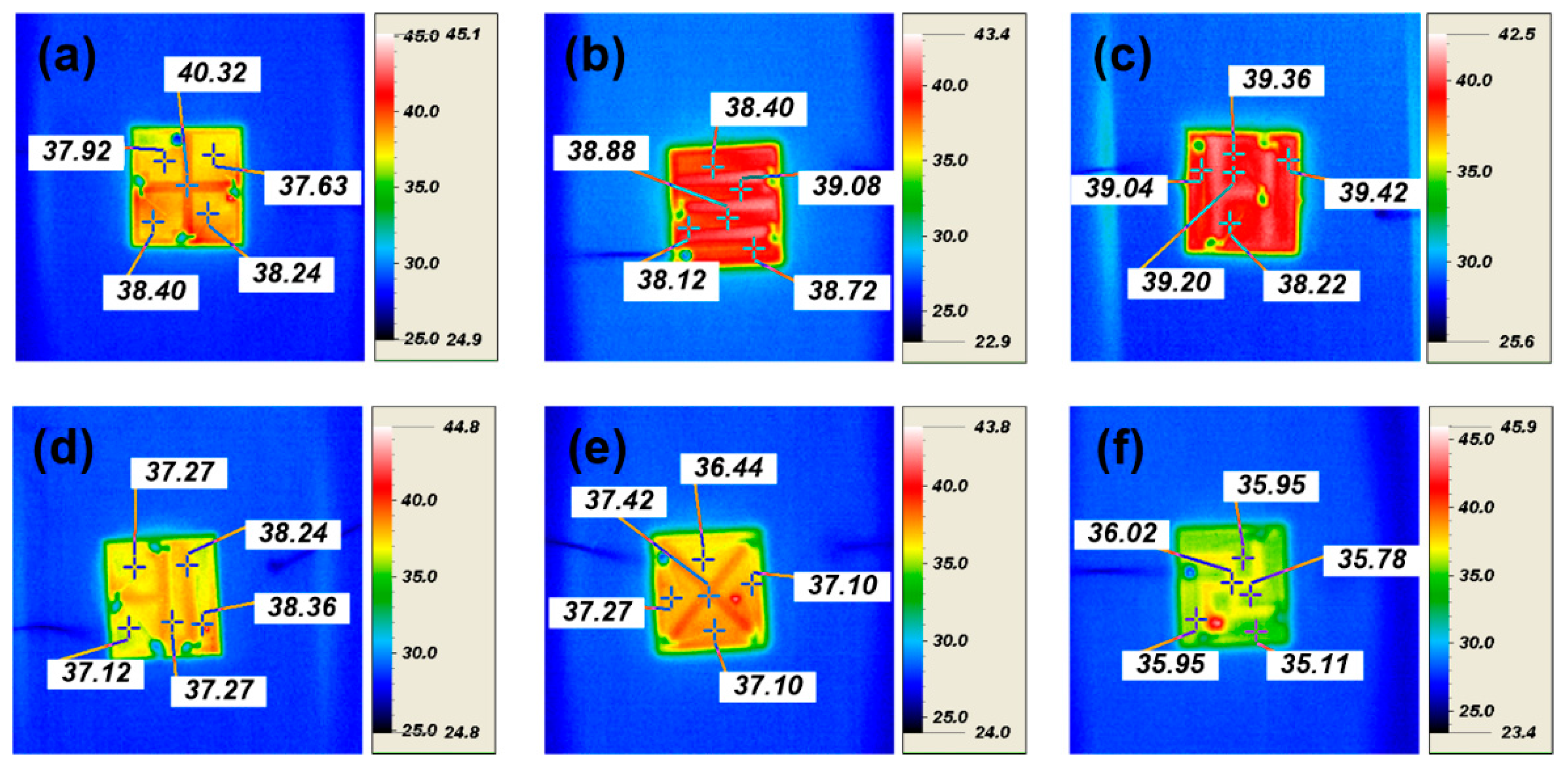
The heat dissipation characteristics of the HV-LEDs can be confirmed through thermal infrared imaging. The surface temperature distributions of Samples A–F are displayed in
Figure 4a–f, respectively, at an injection current of 80 mA. For Samples A–F, the surface temperatures were 37.63–40.32, 38.12–39.08, 38.22–39.42, 37.12–38.36, 36.44–37.42, and 35.11–36.02 °C, whereas the temperature differences were 2.69, 0.96, 1.20, 1.24, 0.98, and 0.91 °C, respectively. Sample F possessed a lower surface temperature and a more uniform temperature distribution. Moreover, the temperature differences of Samples B and E were similar to that of Sample F. The temperature differences of Samples C and D (1.20 and 1.24 °C, respectively) were close to each other. However, in Sample A, a more nonuniform temperature distribution (2.69 °C) was observed. Compared with the electrodes of Samples B–F, the electrodes of Sample A exhibited the greater heat accumulation; the heat accumulation resulted in electrode deterioration, which reduced the reliability and lifetime of the device. In addition, the measured results of surface temperatures for these six samples were in close agreement with those of the spatial distribution images of the light output (
Figure 3).
According to the aforementioned results, Sample E, fabricated using four triangular cells, had the higher light extraction than that of the other samples, which can be attributed to the lower current crowding near the electrodes and a more uniform light emission in this device. On the contrary, Sample A, fabricated using four square cells, had the lowest light extraction because of the severe current-crowding phenomenon near the electrodes. Although Sample F, fabricated using four L-shaped cells, had the lower current crowding near the electrodes, its light extraction performance was worse than that of Sample E. As mentioned, in Sample F, the two-line electrode was prepared on a single cell to improve the current spreading. However, the electrode design caused another problem (i.e., the electrode-shading loss effect). Therefore, the light extraction of Sample F was reduced.
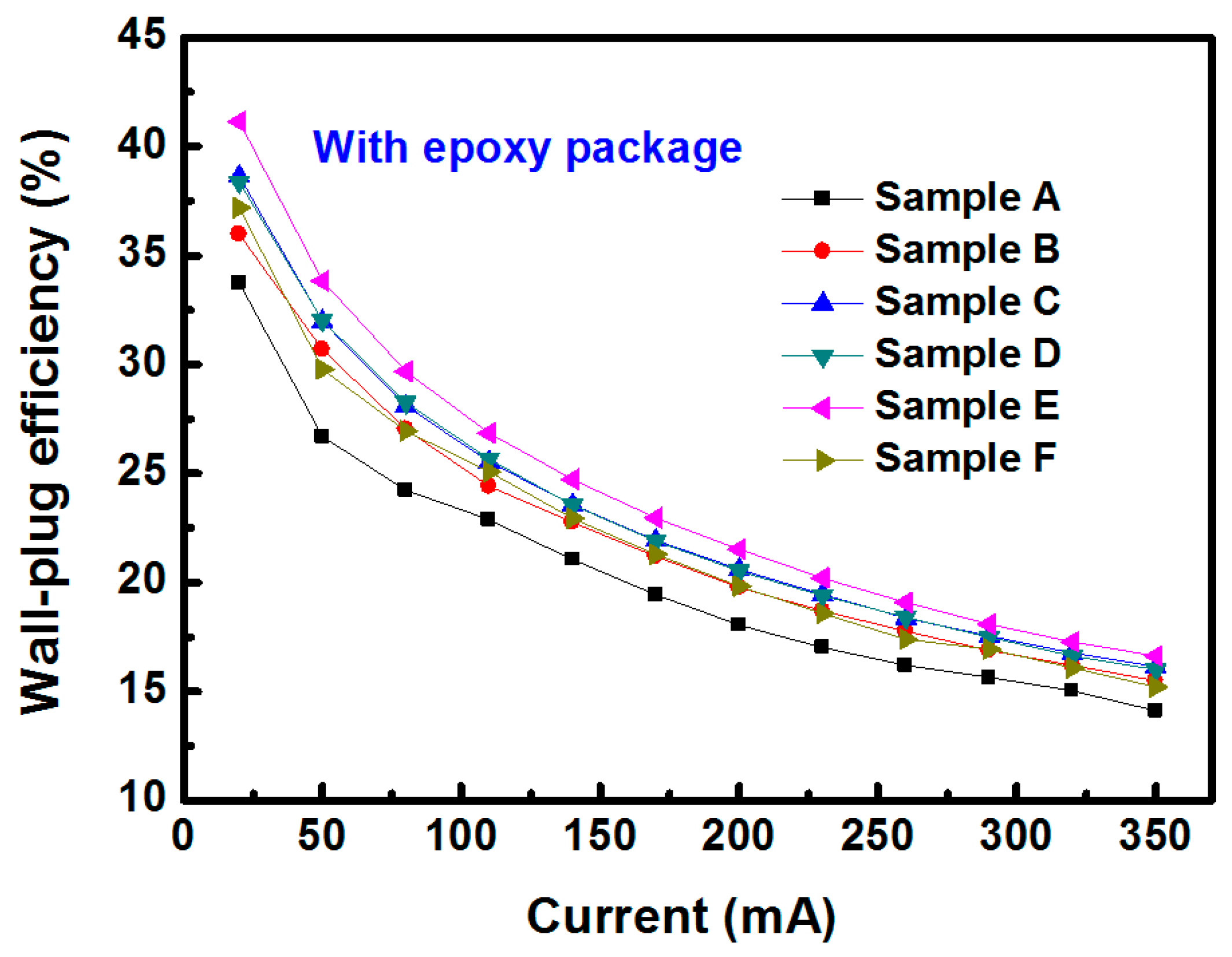
Figure 5 shows the wall-plug efficiencies (WPEs) of epoxy-packaged Samples A–F as a function of injection current of 20–350 mA. The WPEs of packaged Samples A–F at 20 mA were 33.8%, 36.0%, 38.6%, 38.4%, 41.1%, and 37.2%, respectively. The WPEs of these six HV-LEDs at 80 mA were 24.2%, 27.0%, 28.1%, 28.3%, 29.7%, and 26.9%, respectively. The measured results of the I–V characteristics, the light output powers, the spatial distributions of light extraction, and the surface temperatures confirm that the design of Sample E is helpful for improving the optoelectronic performance of vertical HV-LEDs. In addition, this study reveals that the fabrication processes of vertical LED structure are highly feasible for HV-LED applications. At present, the current mass-produced HV-LEDs are almost lateral-type fabricated on sapphire substrates. Due to severe current-crowding and heat-conduction problems, the light output power of the lateral HV-LEDs saturate at ~200 mA. To our knowledge, at an injection current of 80 mA, the highest output power and wall-plug efficiency of current lateral HV-LEDs with epoxy packaging (connected with 2 × 2 micro-cells, micro-cell size: 1016 µm × 1016 µm) are approximately 310.0 mW and 24.8%, respectively. Obviously, at an injection current of 80 mA, the output power and wall-plug efficiency of our vertical HV-LED of Sample E (353.2 mW and 29.7%) possess 13.9% and 19.8% improvements in comparison to those of current lateral HV-LEDs. Because of the favorable heat dissipation of Cu metal substrate, the aid of a reflective mirror layer, the roughness of the n-type GaN surface, and the decrease in the waveguide effect, the optoelectronic performance of vertical HV-LEDs can be improved significantly. In the future, we will fabricate vertical HV-LEDs connected with more cell chips.
4. Conclusions
In this study, laser lift-off and wafer bonding techniques were used to prepare vertical HV-LEDs connected with 2 × 2 micro-cells on Cu substrates. Various cell shapes—such as square, rectangle, triangle, and L shapes—were designed and fabricated on the HV-LEDs. As the HV-LED was connected with four square micro-cells, the electrodes in these micro-cells were all far away from the edges, which induced the severe current-crowding phenomenon. However, when four rectangle, triangle, or L-shaped micro-cells were used to fabricate the HV-LED, the electrodes in these micro-cells were close to the edges, enhancing the current spreading effect. The measured results revealed that the HV-LED with four triangular micro-cells exhibited the higher light extraction and a more uniform light emission than did those with other cell shapes. At injection currents of 20 and 80 mA, the HV-LED with epoxy packaging showed higher light output powers of 102.8 and 353.3 mW, and its WPEs were 41.1% and 29.7%, respectively. Although the HV-LED combined with L-shaped cells exhibited a favorable current spreading effect, the electrode-shading loss effect degraded the light extraction. The triangular cell design can efficiently improve the performance of vertical HV-LEDs. Furthermore, the fabrication techniques of the vertical LED are highly useful for HV-LED applications.


