Abstract
An observation was made in this research regarding the fact that the signatures of isotropic charge distributions in silicon nanowire transistors (NWT) displayed identical characteristics to the golden ratio (Phi). In turn, a simulation was conducted regarding ultra-scaled n-type Si (NWT) with respect to the 5-nm complementary metal-oxide-semiconductor (CMOS) application. The results reveal that the amount of mobile charge in the channel and intrinsic speed of the device are determined by the device geometry and could also be correlated to the golden ratio (Phi). This paper highlights the issue that the optimization of NWT geometry could reduce the impact of the main sources of statistical variability on the Figure of Merit (FoM) of devices. In the context of industrial early successes in fabricating vertically stacked NWT, ensemble Monte Carlo (MC) simulations with quantum correction are used to accurately predict the drive current. This occurs alongside a consideration of the degree to which the carrier transport in the vertically stacked lateral NWTs are complex.
1. Introduction
The golden ratio (commonly referred to as the golden section or golden mean, and denoted by the Greek letter Phi) is noteworthy for a variety of reasons: firstly, it can be observed in many naturally occurring patterns, artistic works, and mathematical phenomena; and secondly, in more recent years, the literature has uncovered specific nanoscale symmetry concealed within solid state matter, which reflects aspects of the golden ratio [1].
Despite the availability of numerous studies that have sought to measure natural instances of the golden ratio, a publication has yet to emergence addressing the effect that Phi has on the central parameters and performance of nano transistors, including gate all around (GAA) nanowire transistors (NWTs) [2]. As illuminated in studies such as [3,4], GAA NTWs constitute a promising device architecture that are anticipated to be used for technological advancement in the domain of nodes. In particular, owing to their favorable property of electrostatic integrity, GAA NTWs have been marked as one of the successors of Fin field effect transistor (FinFET) technology in the 5-nm technology node.
It is possible to establish an ideal compromise between leakage currents and GAA NTW performance by engineering device structures. In fact, the literature indicates that the nanowires’ cross-sectional shape strongly affects NWTs’ gate capacitance and mobile charge [5,6,7]. As a case in point, for an NWT characterized by <110> channel orientation, as well as an extended elliptical cross-section (where the long diameter is parallel to the surface of the silicon wafer), it is associated with the greatest mobile charge for a certain gate voltage. It is noteworthy that one of the key determinants of device performance has been established as the ratio of the major axis to the minor axis (namely, cross-section aspect ratio or AR). Nevertheless, industrial players have tended to only manufacture NWTs in two different versions: circular cylinder (or elliptical) NWTs [8,9] and nanosheet (or nanoslab) FETs [10]. Each version has its own trade-offs; however, the key difference between these two versions is the cross-sectional AR. Several critical design questions, including the optimal NWT cross-sectional aspect ratio, remain unanswered.
To answer this question, the AR of a GAA NWT is changed while the cross-sectional area is kept constant; surprisingly, the signatures of the isotropic/anisotropic charge distributions are observed as showing the same attributes as the golden ratio.
The immediate aim of the present research is to examine the distinctive structural and dimensional features of the transistors associated with 5-nm Si CMOS technology, thereby illuminating the quantum mobile charge to gate capacitance ratio [5,7], where the indicator of the intrinsic speed of the NWT is the intrinsic delay (τ) [11]. For the purpose of heightening the degree to which the obtained results are realistic, the simulations take into consideration the effect of quantum confinement, non-equilibrium transport, and contact resistance for such ultra-scaled NWTs. An examination of the correlation between the golden ratio and 5 nm NWT performance is also made to take into account the effect of the main sources of statistical variability (SV) [12].
The early successes of fabrication of vertically stacked lateral NWTs may help resolve degradation of the drive current per footprint while shrinking the contacted gate pitch at the 5 nm node [9,10]. The vertically stacked NWTs have also been included in the international technology roadmap for semiconductors (ITRS) roadmap [13]. In an attempt to determine the performance of vertically stacked of NWT with golden AR, the quantum correction achieved by Poison-Schrödinger was used together with non-equilibrium transport to calibrate the drift-diffusion of a single NWT [14,15]. The calibrated drift diffusion (DD) was then used to simulate the vertically stacked lateral NWTs.
2. Device Description
In this study, two NWT structures are used; single lateral NWTs and vertically stacked lateral NWTs. The purpose is to determine the optimal AR, and Figure 1 shows a 3D representation and material details for the initial structure of the NWTs. The Si channel is wrapped in a 0.4 nm SiO2 interfacial layer and a 0.8 nm HfO2 (High-k) layer is added at the gate region. The doping concentration in the channel is 1014/cm3, in the extensions 1020/cm3, and in the source/drain 4 × 10²⁰/cm3. The charge transport’s direction is organized along with x-axis, and Table 1 outlines the cross-sectional dimensions for 9 elongated elliptical nanowires (each with the same cross-sectional area amounting to approximately 10π nm2). In addition, the diameter of the NWT along the y-axis ranges from 4.44 nm to 9.0 nm, whereas the matching diameter along the z-axis ranges from 9.0 nm to 4.44 nm. Resultantly, variance with respect to the matching aspect ratio is from 2.020 to 0.490. It should also be noted that the cross-sectional dimensions include wires with Phi and 1/Phi values. For the estimation of NWTs’ performance after determining the optimal AR, state-of-the-art technology keys such as source/drain doping profile, predictive contact resistance, and gate length were utilized for both single NWT and vertically stacked lateral NWT structures.
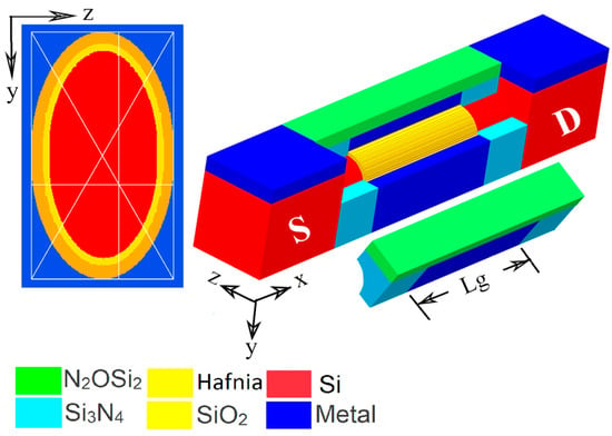
Figure 1.
Three-dimensional representation of Si-NWTs (with cross-sectional dimensions of 5 nm × 8.1 nm), as well as chemical constituents. The straight, white lines indicate that golden ratio (Phi) can be observed on the cross-sectional slice with respect to the middle of the nanowire transistors (NWT) channel.

Table 1.
Simulated devices’ physical cross-section dimensions.
3. Methodology
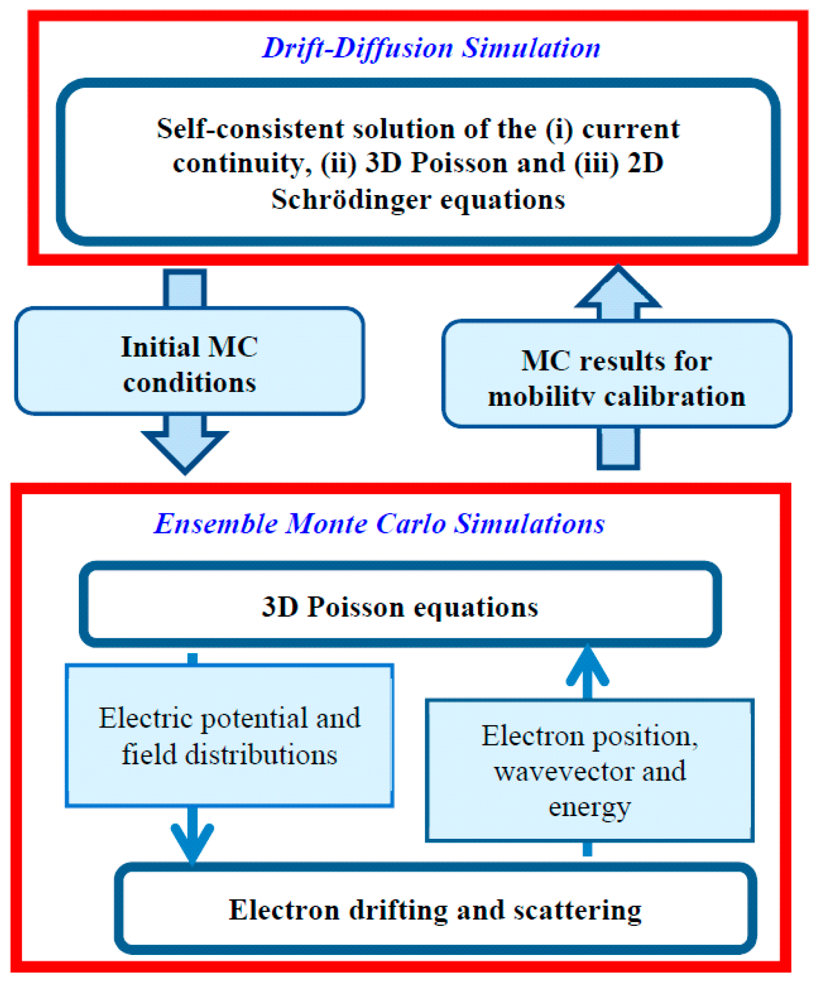
In conjunction with the three-dimensional Monte-Carlo (MC) and drift-diffusion (DD) simulation techniques [12,16], this paper draws on Poisson-Schrödinger (PS) quantum corrections [17,18]. See Figure 2 for the author’s approach to simulation. As will be clear to the reader, the quantum-corrected MC simulations, which valuably reflect the non-equilibrium transport effects [17,19,20,21,22], generate predictive simulation results. After conducting the DD simulations and, in turn, calibrating these in view of the MC results, the former can be used to reflect the contact resistance impacts [4]. Furthermore, it is possible to use the calibrated DD simulations to examine relative changes in Ion, thus facilitating design optimization and, in addition to this, the creation of efficient statistical variability (SV) and statistical reliability (SR) simulations [12,23,24].
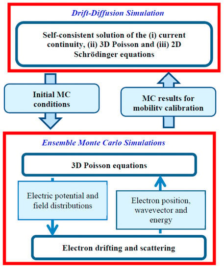
Figure 2.
Flowchart for the overall simulation method. MC: Monte-Carlo.
4. Results and Discussions
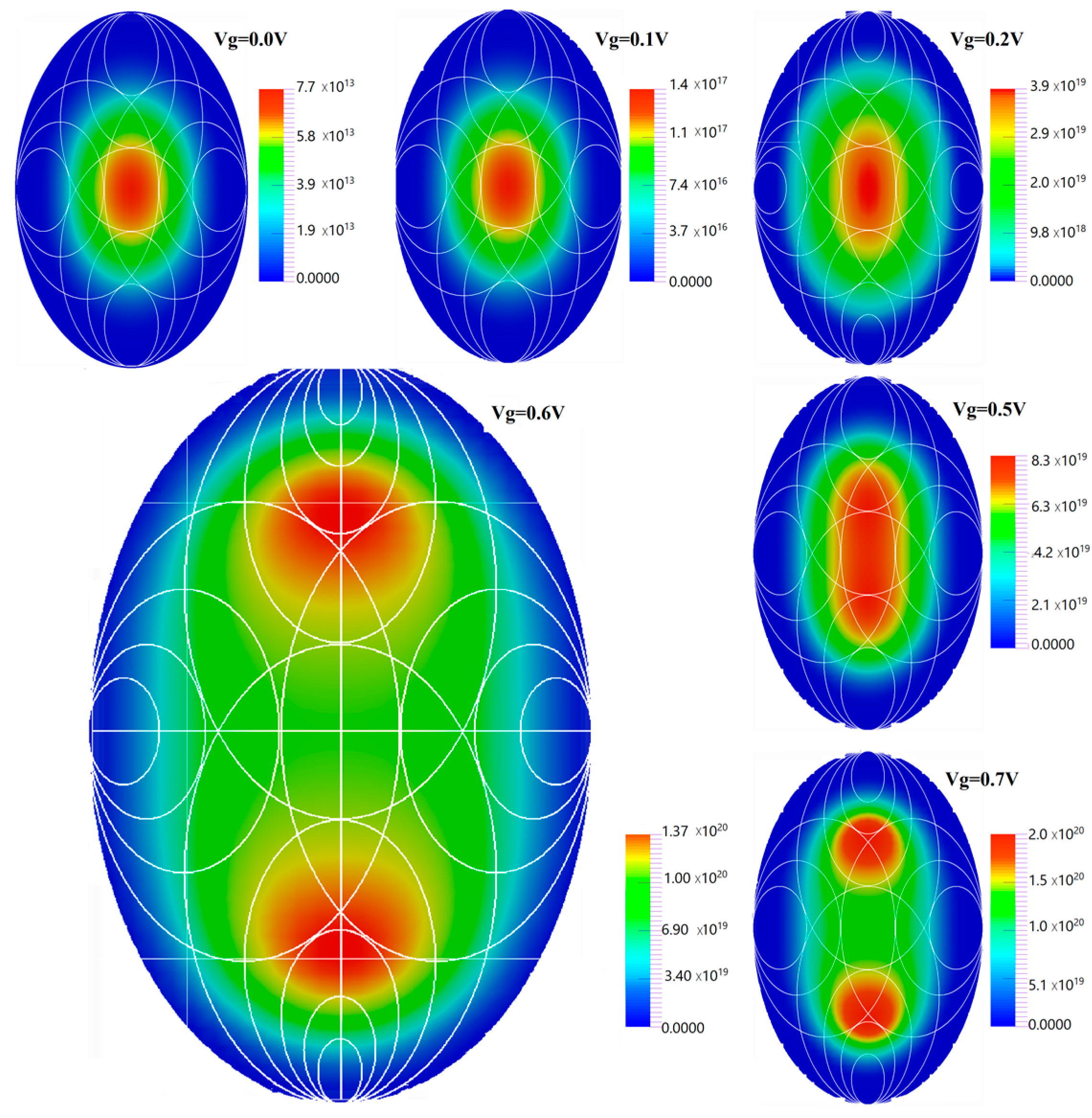
The PS quantum corrections offer a precise charge distribution within the simulated NWTs’ channel [5]. And Figure 3 gives the Phi ovals represented on a two-dimensional cross-section at the center of the gate. It is noteworthy that patterns of isotropic charge distribution derived from the PS simulations are comparable (in terms of their characteristics) to Phi, and despite the voltage-dependent nature of the charge distributions, the Phi ovals’ signatures can be identified at every gate voltage.
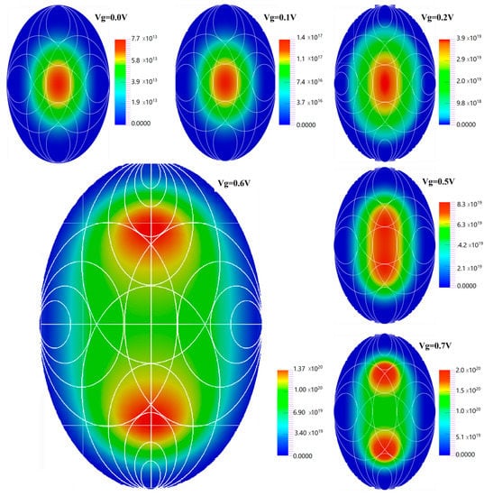
Figure 3.
The Poisson-Schrödinger (PS) simulations’ charge distribution results. Here, the Phi ovals (marked in white) emphasize the comparability between the golden ratio and the charge distribution within the 5 nm × 8.10 nm NWT cross-section. The slice cut is at the middle of NWT channel at gate bias (0, 0.1, 0.2, 0.5, 0.6, 0.7) Volt at high drain voltage VD = 0.7 V. The gate length Lg = 12 nm.
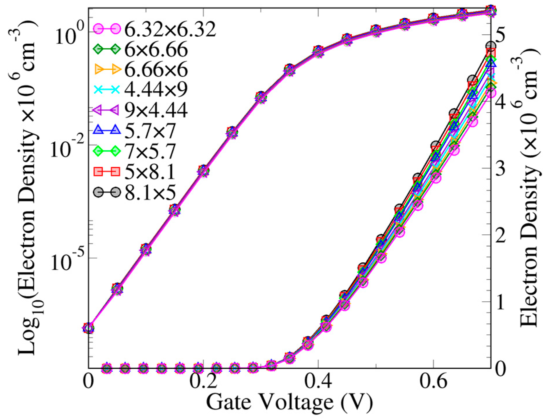
For the purpose of evaluating the effect that the NWT cross-section dimension has on device performance in a reasonable manner, Figure 4 gives the gate voltage against the quantum mobile charge within the channel (for the initial 9 NWTs given in Table 1). Here, the alignment of the QM-VG curves takes place by altering the gate work function, and the reader should recognize that the mobile charge is predicted in the middle of the channel. Perhaps the centrally interesting result to arise from our consideration of the QM-VG attributes in Figure 4 relates to the fact that the greatest level of quantum charge is associated with NWTs which have the Phi and 1/Phi dimensional ratios. When comparatively examined against every other elliptical device, the NWT whose cross-section is precisely circular is associated with the lowest level of quantum charge.
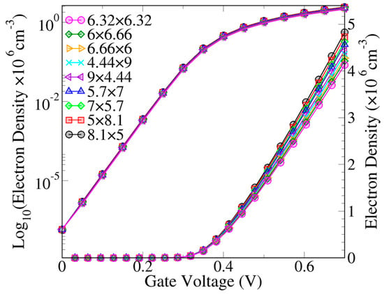
Figure 4.
9 NWT cross-section aspect ratios and the gate voltage dependence of the NWTs’ quantum mobile charge. The crystallographic Silicon (Si) channel orientation is <110>. Each NWT has cross-sectional area ≈10π nm2. The gate length = 12 nm.
In Table 2 and Table 3, a certain gate voltage (VG) is used for the <110> and <100> crystallographic orientations, thus facilitating a comparative examination of the simulated gate capacitance (CG) and mobile quantum charge in the channel per-unit-length (QM). QM is in a direct and proportional relationship to the NWT gate capacitance, in view of the following equation:
where VT and VG denote the threshold voltage and gate voltage, respectively.

Table 2.
Quantum charge to the gate capacitance ratio at identical QM at zero gate bias (for NWTs with crystallographic Silicon channel orientation <110>.

Table 3.
Quantum charge to the gate capacitance ratio at identical QM at zero gate bias (for NWTs with crystallographic Silicon channel orientation <100>.
In view of this, it is reasonable to conclude that the fall in NWT gate capacitance brings about an attendant fall in the channel’s mobile charge, thus reducing the overall level of transistor performance. In view of the information given in Table 2 and Table 3, it is evidently the case that for the two crystallographic orientations, capacitance is greatest when the wires reflect Phi. As for the wires with the <100> crystallographic orientation, the charges in the Phi and 1/Phi instances are exactly the same, which can be accounted in reference to the mY and mZ effective masses (of electrons).
Hence, it could conceivably be hypothesized that the two recent successful industrial attempts to build NWTs with cross-sectional AR ≈ 1 (circular NWT [8,9] and AR ≈ 3.5 (sheet NWT) [10] have overlooked the fact that AR contributes to NWT performance (in this study, the term “sheet NWT” refers to any NWT where 0.5 ≥ AR ≥ 2).
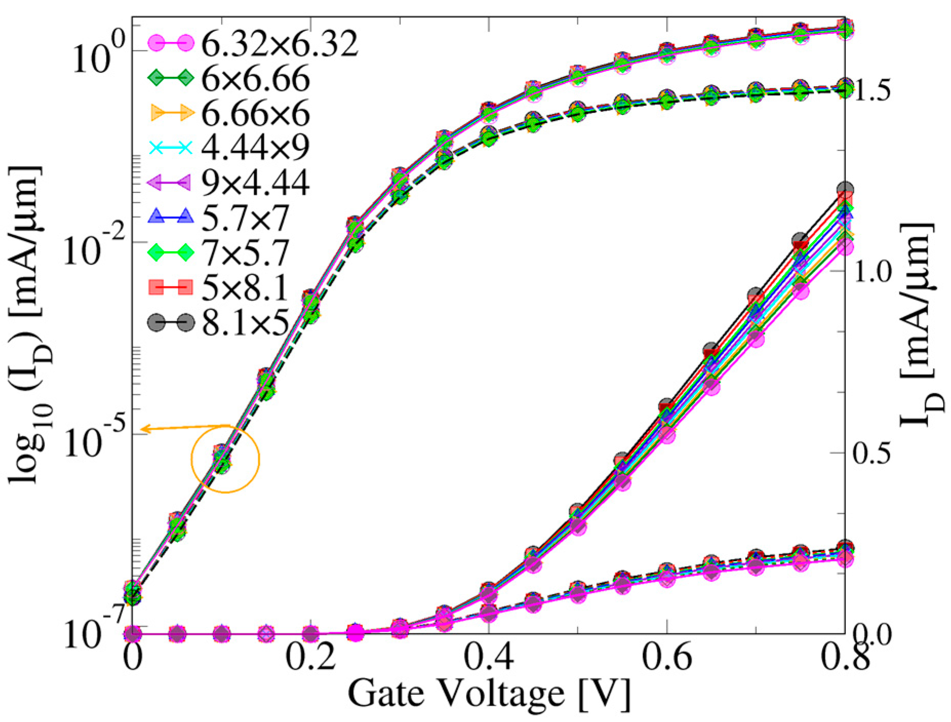
Figure 5 compares the effect of 9 cross-section aspect ratios for Si NWTs on the ID-VG curves. Consistent with the data presented so far, the NWTs with cross-sections equal to 1/Phi and Phi own the highest Ion at low drain voltage as well as at high drain voltage.
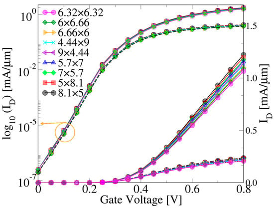
Figure 5.
The effect of 9 cross-section aspect ratios for Si NWTs on the ID-VG curves. Dotted lines represent a low drain voltage (namely, VD = 0.05 V), whereas continuous lines represent a high drain voltage (namely, VD = 0.7 V). <110> is the channel orientation for Si, while the gate length amounts to 12 nm.
In Figure 6, it is clear that τ constitutes a function of LG. In particular, τ is correlated in a direct way to the device’s speed, where the NWTs’ speed with respect to τ can be expressed as follows:
where CG represents the total gate capacitance; Ioff = (IH + IL)/2 represents the effective current, where IH = ID (VG = VDD, VD = VDD/2), and IL = ID (VG = VDD/2, VD = VDD). VDD = 0.6 V, and the leakage current is Ioff = 0.6 µA/µm. Figure 6 illustrates that NTWs with 8.10 nm × 5 nm and 5 nm × 8.10 nm are associated with the lowest value of τ, and the evaluation of τ is consistent with the QM/CG results (see Table 2).
τ = CG(VDD/Ioff)
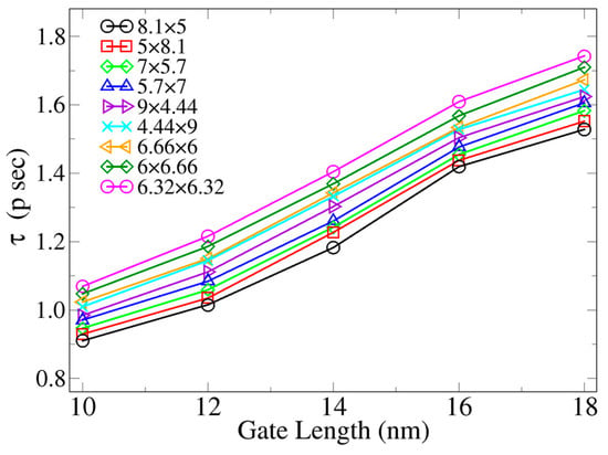
Figure 6.
LG with respect to τ for NWTs with varying cross-section aspect ratios (including Phi and 1/Phi). The Si channel orientation is <110>.
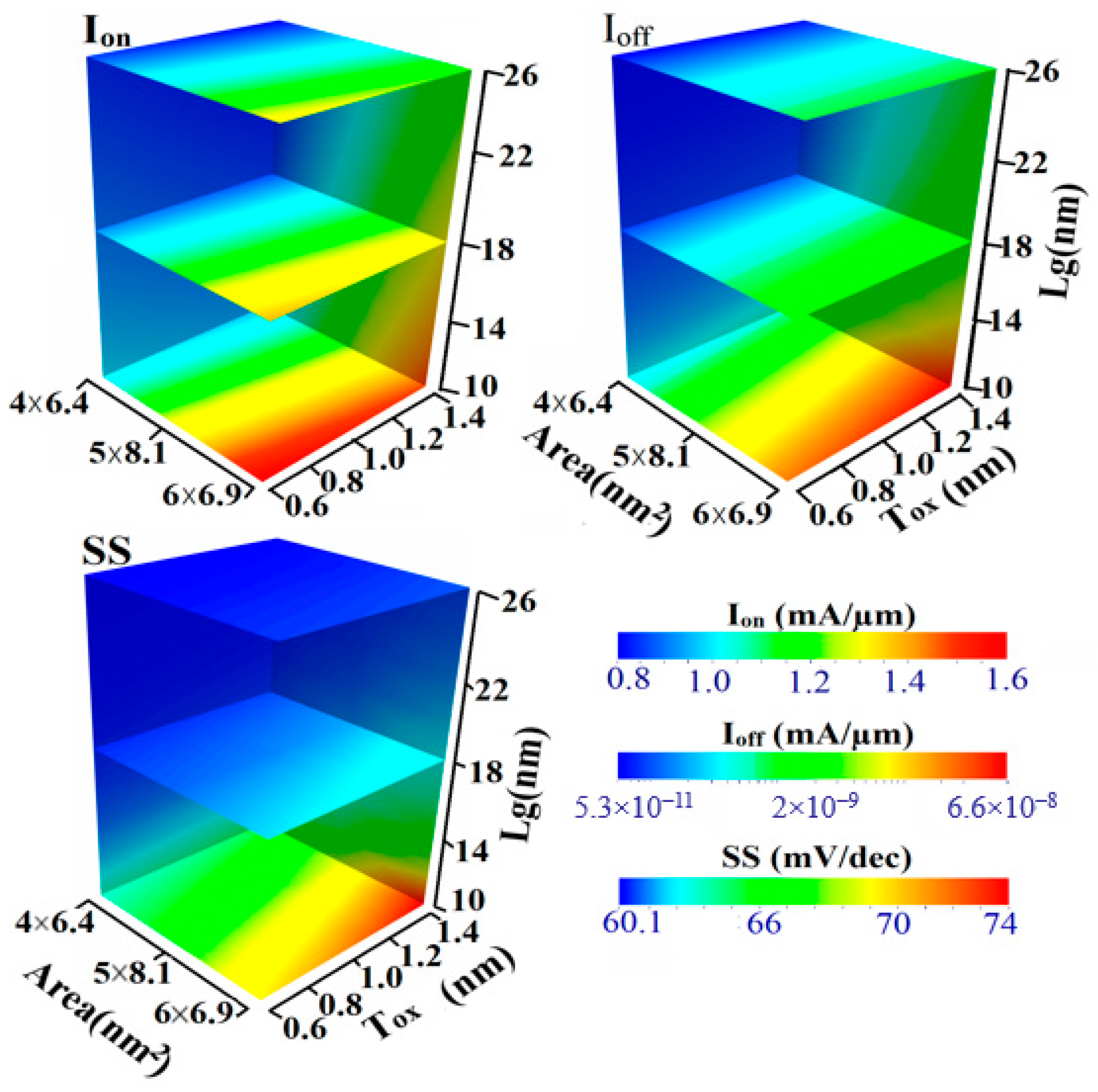
A much more systematic design of experiments would identify how NWTs’ FOMs interact with other variables that are correlated to AR. Figure 7 shows a possible design of such experiments, including the effect of gate lengths and oxide thickness, and NWT cross-sectional dimensions on Ioff, Ion and sub-threshold slope (SS). As this study concentrates on 5 nm NWT, three-cross-sectional areas with golden ratios are involved in the design of these experiments: (4 nm × 4.6 nm), (5 nm × 8.1 nm), and (6 nm × 6.9 nm), with corresponding cross-sectional-areas 4.6π, 10.125π, and 10.35π (nm2). In all cases, only <110> channel orientation is considered.

Figure 7.
Experimental design for investigation of the impact of NWT size, LG, and oxide thickness on drain-induced barrier lowering (DIBL), Ioff, Ion, and VT.
As in a tri gate (FinFETs) the on-current is closely proportional to the fin height of the fin or NWT diameter [25,26] In view of the simulation results, it is possible to conclude that the greatest value of the drive current is associated with the NWT characterized by the shortest gate length and, furthermore, the thinnest oxide. The SS reflects the electrostatic integrity of the transistors. The NWT with a long channel and narrow dimensions has better gate control, resulting in a steeper SS.
The key problem with ultra-scaled NWTs is the challenge of performance degradation, seen as degradation in the Ion per lay-out pitch Ion A/µm while maintaining low off-state leakage. Paired with altering NWT geometric features, along with crystallographic orientation, it is possible to enhance the electron transport attributes in Si NWTs by establishing a strain in the channel [27,28,29].
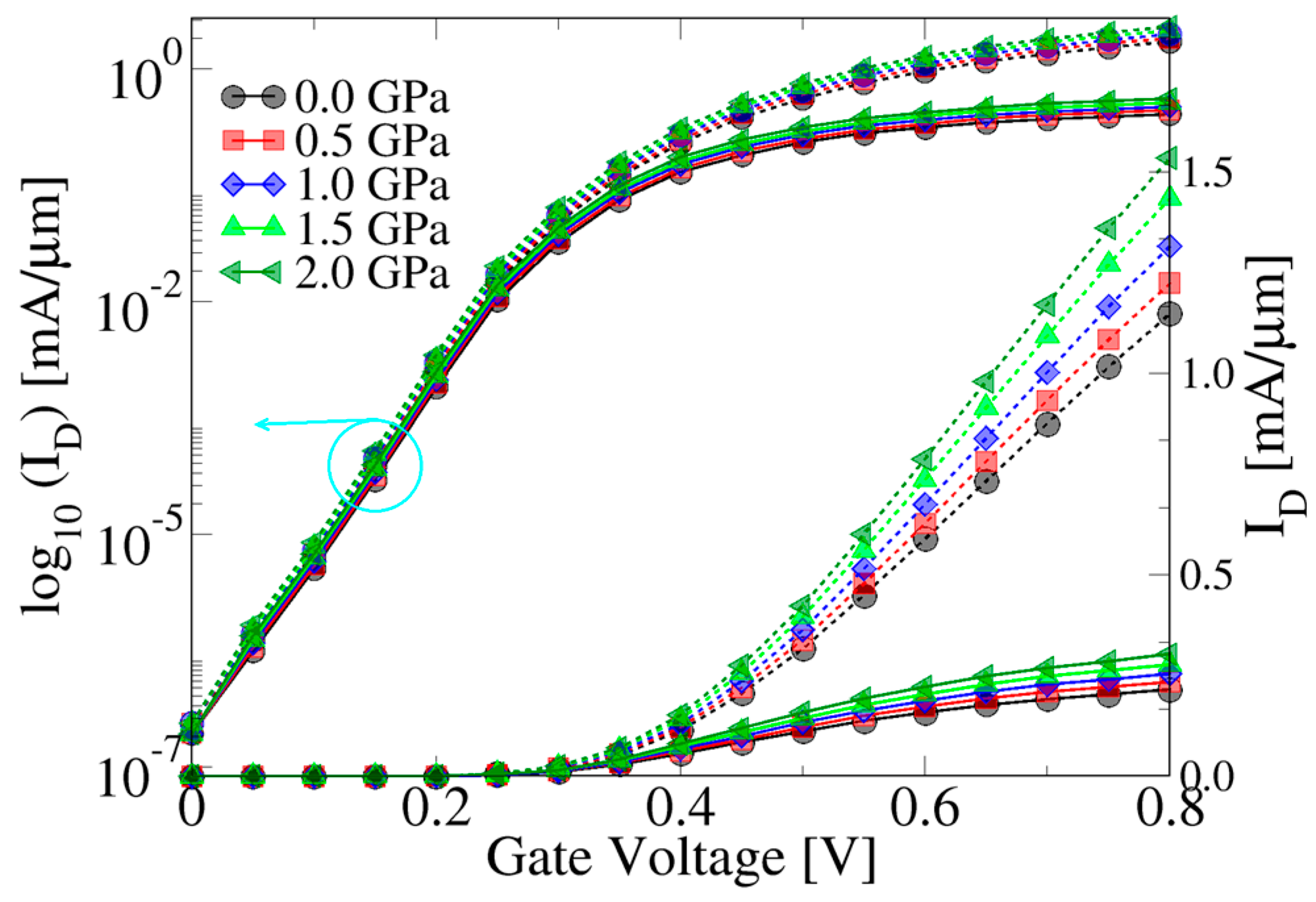
In Figure 8, the results are given for the simulated ID-VG characteristics of a NWT (5 nm × 8.10 nm [Phi]) with a crystallographic orientation of <110> at several tensile strain values. Evidently, in the 5% to 30% range, establishing a strain in the channel has a beneficial impact on the saturation current magnitude. Furthermore, establishing a 2 GPa tensile strain has a positive impact on NWT performance (approximately 30%) when considered in relation to the unstrained NWT. Nevertheless, the Ion barely reaches the margin of the industrial target for 5 nm node; hence, contact resistance is neglected in this case.
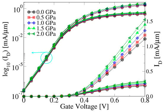
Figure 8.
ID-VG curve plotted of the 5 nm × 8.10 nm strained silicon NWT at several channel strains. Dotted lines represent VD = 0.7 V, whereas continuous lines represent VD = 0.05 V. Crystallographic orientation of the Si channel is <110> and LG = 12 nm.
Variability in the context of contemporary nanoscale transistor science is an increasingly important context, especially in view of process deviation and the inherent attributes of semiconductor materials and interfaces. Although the NWT with Phi cross-sectional AR has unique attractive features, it is useful to compare, in detail, the impact of the individual and combined local statistical variability sources on such an NWT. Statistical variability (SV) is given rise to by numerous variables, including random discrete dopants (RDD), metal gate granularity (MGG), and wire edge roughness (WER), all of which serve to predominate within NWT behavior.
Figure 9 gives VT, Ion, DIBL, and Ioff distributions subject to combined SV (RDD, WER, and MGG), all of which are reflective of the gate-first technology of the NWTs listed in Table 2. Comparing the normal distribution of ensembles of 1000 microscopically different transistors simulated for each one of the nine NWTs, it can be seen that the distributions are close to Gaussian. Furthermore, the normal distributions are shifted in consistency with results of ID-VG characteristics in Figure 5, hence causing the Phi and 1/Phi ratio NWTs to have better Ion, DIBL, VT, and Ioff results. This may be explained by the fact that NWTs with Phi and 1/Phi ratios have better electrostatic integrity and more mobile charge and gate capacitance.
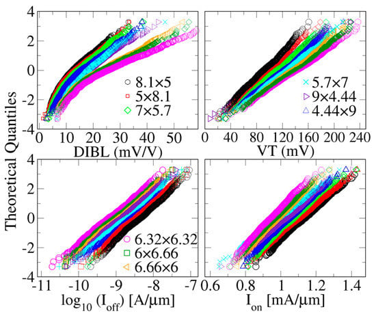
Figure 9.
VT, Ion, DIBL, and Ioff distributions subject to combined SV (RDD, WER, and MGG), all of which are reflective of the gate-first technology of the NWTs listed in Table 2.
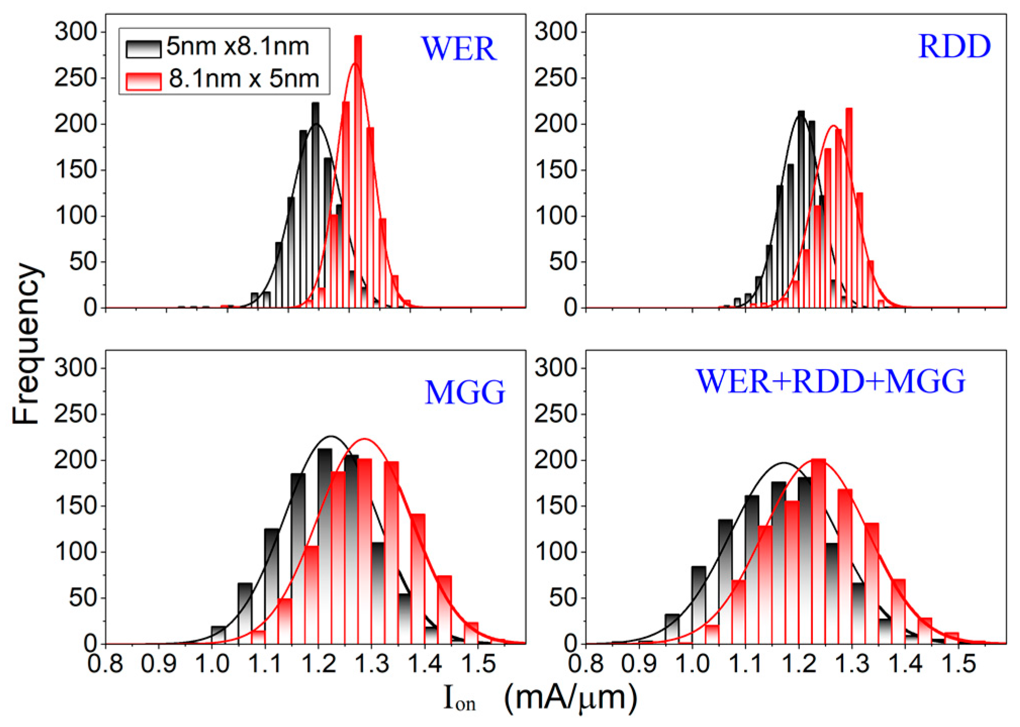
One of the most significant findings to emerge from these simulations is that Phi and 1/Phi ratios can thus be suggested as offering the optimal AR. The VT and Ion variability depends on the parameters of the variability sources, and thus further investigations to assess the effects of individual SVs for Phi and 1/Phi NWTs on VT and Ion are required. For each individual source, and for their combinations, ensembles of 1000 microscopically different transistors are thus simulated as shown in Figure 10 and Table 4. The effects of SV sources on Ion of Phi NWTs are similar to those of 1/Phi NWTs, with a 0.1 mA/µm shift in Gaussian distribution. This shift has relevance as the mobile charge QM in the channel of 1/Phi NWTs is higher than QM in the channel of Phi NWTs. Another important implication is that the Ion standard deviation of the 1/Phi NWTs is less than in the Ion SD of Phi NWTs for <110> channel orientation. Further, MGG is significantly wider in Ion variability than other SV sources. These findings are also valid for threshold voltage variability as shown in Figure 11 and Table 5.
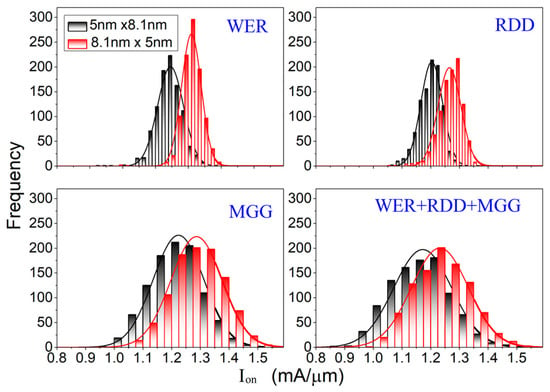
Figure 10.
Ion distributions subject to combined individual SV and combined SV (RDD, WER, and MGG) which are representative of gate-first technology of Phi and 1/Phi NWTs.

Table 4.
Mean and standard deviation values of Ion, subject to combined individual SV and combined SV (RDD, WER, and MGG) which are representative of gate-first technology of Phi and 1/Phi NWTs.
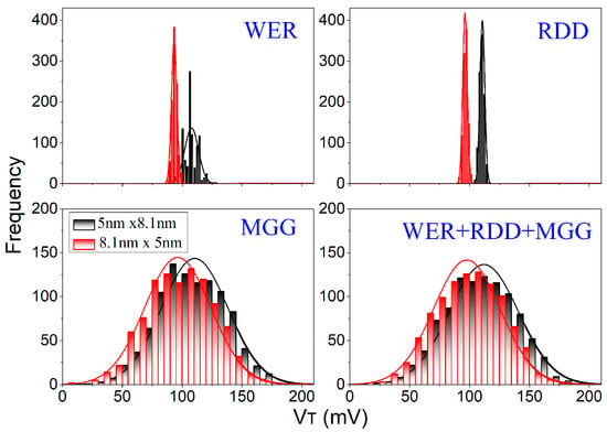
Figure 11.
Threshold voltage (VT) distributions subject to combined individual SV and combined SV (RDD, WER, and MGG) which are representative of gate-first technology of Phi and 1/Phi NWTs.

Table 5.
Mean deviations and standard deviations values of VT subject to combined individual SV and combined SV (RDD, WER, and MGG) which are representative of gate-first technology of Phi and 1/Phi NWTs.
Presented in Figure 12 are the distribution and correlations between extracted figures of merit (FoM), derived from the TCAD simulations conducted with respect to the degraded NWT with a trap sheet density amounting to 1 × 10¹² /cm2 when variability sources (RDD, WER, MGG) are considered. Both figures show a correlation between the VT, Ioff, and Ion. However, nevertheless, the correlation between DIBL and the remaining FoM is weak.
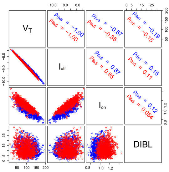
Figure 12.
VT, Ion, DIBL, and Ioff distributions subject to combined SV (RDD, WER, and MGG), all of which are reflective of the gate-first technology of the NWTs given in Table 2.
The most obvious finding to emerge from the comparison of phi and 1/Phi NWTs is that the 1/Phi NWT has better Ion and therefore could be faster; however, the most important limitation lies in the fact that its footprint is wider than the Phi NWT, which has a negative effect on CMOS device density.
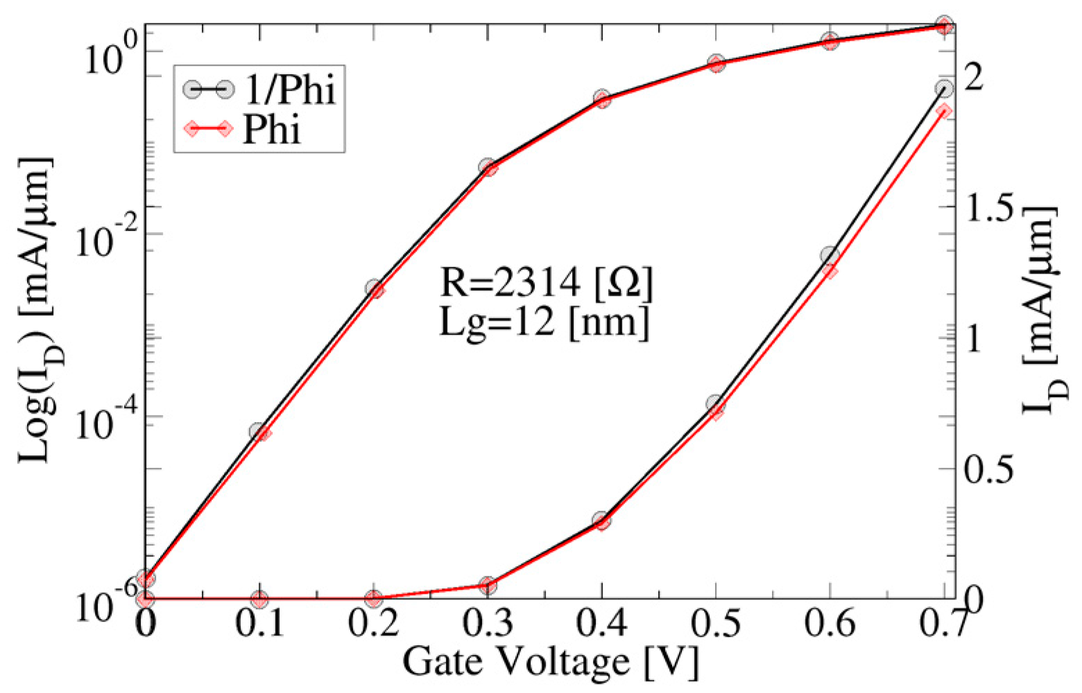
Recent developments in doping technology have exceeded 1021 cm [30], and such heavy S/D doping could also enhance the drive current. Nevertheless, contact resistance remains one of the greatest challenges for 5 nm technology. Figure 13 compares the Ion of Phi NWTs with S/D doping up to 1.2 × 1021 cm−3, with contact resistance in the range (500–2500) Ω, and gate length (10–22) nm. At the predictive Lg = 12 nm and R = 2314 Ω of the 5 nm node [26,31,32], Figure 13 shows the Ion as 1.4 mA/µm.
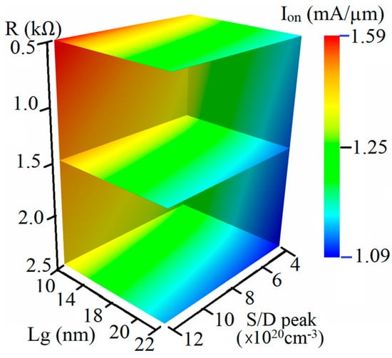
Figure 13.
Correlation between NWT performance and source/drain peak doping, gate length, and S/D contact resistance. NWT cross-section is Phi (5 nm × 8.1 nm) and channel orientation is <110>. Ion extracted at high drain voltage VD = 0.7 V.
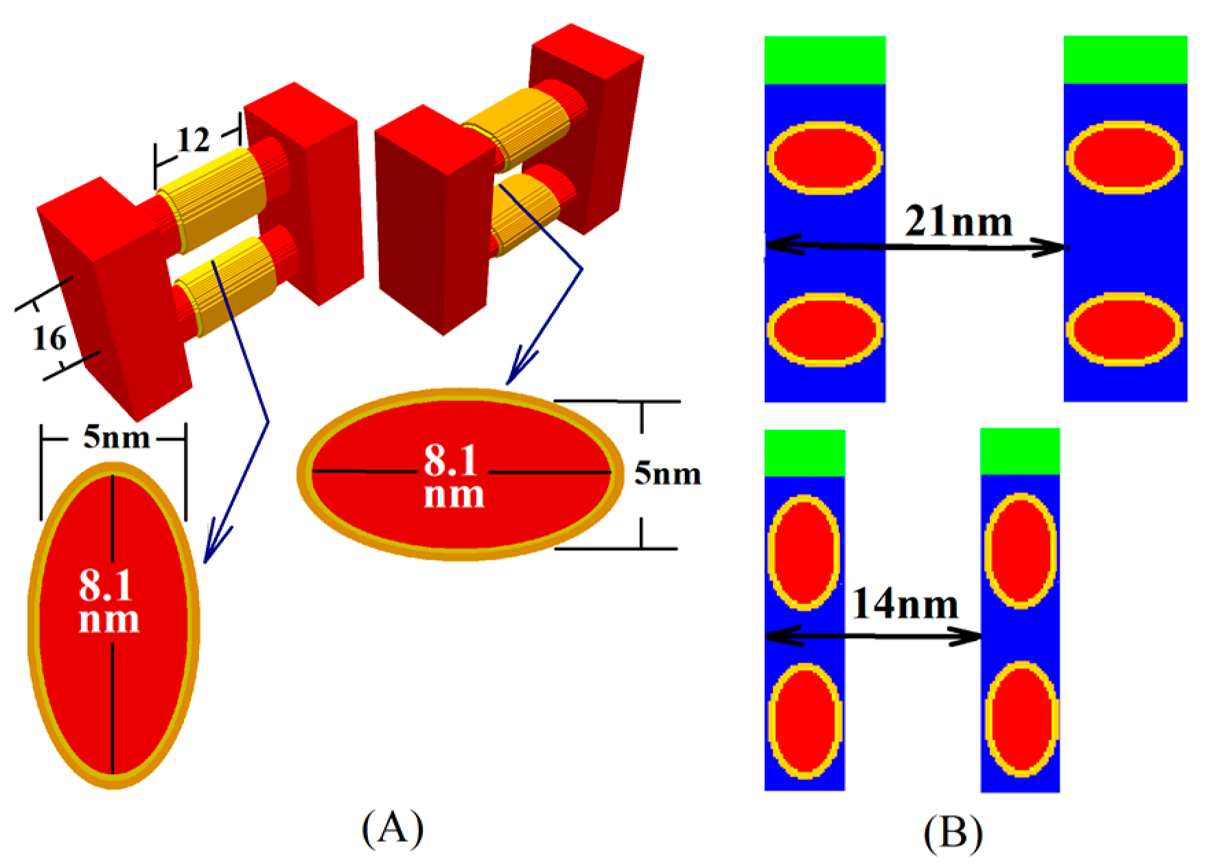
Vertically stacked lateral NWT nanowires are included in the ITRS roadmap to reduce the contacted gate pitch and to enhance the current per footprint. Figure 14 compares both Phi and 1/Phi NWTs in vertically stacked structures. The ID-VG characteristics of both NWTs are shown in Figure 15.

Figure 14.
(A) Vertically stacked lateral NWT of both phi and 1/Phi; (B) The gate pitch layout for Phi and 1/Phi NWTs.
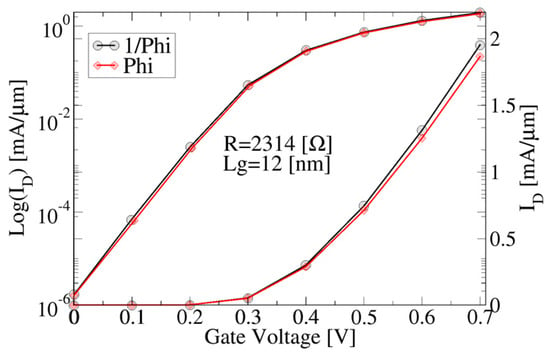
Figure 15.
ID-VG characteristics of vertically stacked of two lateral Phi (5 nm × 8.1 nm) (red) and (8.1 nm × 5 nm) 1/Phi (black) NWTs at high drain voltage VD = 0.7 V. The gate length is 12 nm. <110> is the channel orientation.
5. Conclusions
The present paper represents a valuable contribution to the literature, since it is the first publication to deal with a simulation of the effect that Phi has on the electrostatics and device performance of n-type silicon nanowire transistors for 5-nm CMOS applications. Regarding the main findings, it is reasonable to conclude that the usage of NWT shapes with aspect ratios equivalent (or approximate) to Phi has the potential to serve as a way to enhance gate capacitance, along with the mobile charge in the channel. In view of this, significant potential exists to heighten the intrinsic speed of the device. Noteworthy findings are also enclosed regarding the relationship between gate length and time delay, along with the main FoM, including VT, Ioff and Ion, and DIBL.
Acknowledgments
The author is grateful for the support given by the European Union Horizon 2020 research and innovation program SUPERAID7 (Stability Under Process Variability for Advanced Interconnects and Devices Beyond 7 nm node) under grant agreement No. 688101. Talib Al-Ameri is also grateful for the support given by Al-Mustansiriyah University and the Iraqi Ministry of Higher Education and Scientific Research. I’d like to thank Professor Asen Asenov, for his support and encyclopedic knowledge of nanotransistors modelling. I’d also like to thank, Fikru Adamu-Lema and Vihar Georgiev for all their help.
Conflicts of Interest
The author declare no conflict of interest.
References
- Coldea, R.; Tennant, D.A.; Wheeler, E.M.; Wawrzynska, E.; Prabhakaran, D.; Telling, M.; Habicht, K.; Smeibidl, P.; Kiefer, K. Quantum Criticality in an Ising Chain: Experimental Evidence for Emergent E8 Symmetry. Science 2010, 327, 177–180. [Google Scholar] [CrossRef] [PubMed]
- Al-Ameri, T.; Georgiev, V.P.; Adamu-Lema, F.; Asenov, A. Does a nanowire transistor follow the golden ratio? A 2D Poisson-Schrödinger/3D Monte Carlo simulation study. In Proceedings of the International Conference on Simulation of Semiconductor Processes and Devices (SISPAD), Kamakura, Japan, 7–9 September 2017; pp. 57–60. [Google Scholar]
- Asenov, A.; Wang, Y.; Cheng, B.; Wang, X.; Asenov, P.; Al-Ameri, T.; Georgiev, V.P. Nanowire transistor solutions for 5 nm and beyond. In Proceedings of the 17th International Symposium on Quality Electronic Design (ISQED), Santa Clara, CA, USA, 15–16 March 2016; pp. 269–274. [Google Scholar]
- Al-Ameri, T.; Georgiev, V.P.; Adamu-Lema, F.; Asenov, A. Simulation Study of Vertically Stacked Lateral Si Nanowires Transistors for 5-nm CMOS Applications. IEEE J. Electron Devices Soc. 2017, 5, 466–472. [Google Scholar] [CrossRef]
- Wang, Y.; Al-Ameri, T.; Wang, X.; Georgiev, V.P.; Towie, E.; Amoroso, S.M.; Brown, A.R.; Cheng, B.; Reid, D.; Riddet, C.; et al. Simulation Study of the Impact of Quantum Confinement on the Electrostatically Driven Performance of n-type Nanowire Transistors. IEEE Trans. Electron Devices 2015, 62, 3229–3236. [Google Scholar] [CrossRef]
- Al-Ameri, T.; Wang, Y.; Georgiev, V.P.; Adamu-Lema, F.; Wang, X.; Asenov, A. Correlation between gate length, geometry and electrostatic driven performance in ultra-scaled silicon nanowire transistors. In Proceedings of the 2015 IEEE Nanotechnology Materials and Devices Conference (NMDC), Anchorage, AK, USA, 13–16 September 2015; pp. 1–5. [Google Scholar]
- Al-Ameri, T.; Georgiev, V.P.; Sadi, T.; Wang, Y.; Adamu-Lema, F.; Wang, X.; Amoroso, S.M.; Towie, E.; Brown, A.; Asenov, A. Impact of quantum confinement on transport and the electrostatic driven performance of silicon nanowire transistors at the scaling limit. Solid State Electron. 2017, 129, 73–80. [Google Scholar] [CrossRef]
- Mertens, H.; Ritzenthaler, R.; Chasin, A.; Schram, T.; Kunnen, E.; Hikavyy, A.; Ragnarsson, L.-A.; Dekkers, H.; Hopf, T.; Wostyn, K.; et al. Vertically stacked gate-all-around Si nanowire CMOS transistors with dual work function metal gates. In Proceedings of the 2016 IEEE International Electron Devices Meeting (IEDM), San Francisco, CA, USA, 3–7 December 2016; pp. 19.7.1–19.7.4. [Google Scholar]
- Mertens, H.; Ritzenthaler, R.; Hikavyy, A.; Kim, M.S.; Tao, Z.; Wostyn, K.; Chew, S.A.; De Keersgieter, A.; Mannaert, G.; Rosseel, E.; et al. Gate-all-around MOSFETs based on vertically stacked horizontal Si nanowires in a replacement metal gate process on bulk Si substrates. In Proceedings of the 2016 IEEE Symposium on VLSI Technology, Honolulu, HI, USA, 14–16 June 2016; pp. 1–2. [Google Scholar]
- Loubet, N.; Hook, T.; Montanini, P.; Yeung, C.-W.; Kanakasabapathy, S.; Guillom, M.; Yamashita, T.; Zhang, J.; Miao, X.; Wang, J.; et al. Stacked nanosheet gate-all-around transistor to enable scaling beyond FinFET. In Proceedings of the 2017 Symposium on VLSI Technology, Kyoto, Japan, 5–8 June 2017; Volume 5, pp. T230–T231. [Google Scholar]
- Na, M.H.; Nowak, E.J.; Haensch, W.; Cai, J. The effective drive current in CMOS inverters. In Proceedings of the Digest. International Electron Devices Meeting, San Francisco, CA, USA, USA, 8–11 December 2002; pp. 121–124. [Google Scholar]
- Asenov, A.; Brown, A.R.; Davies, J.H.; Kaya, S.; Slavcheva, G. Simulation of intrinsic parameter fluctuations in decananometer and nanometer-scale MOSFETs. IEEE Trans. Electron Devices 2003, 50, 1837–1852. [Google Scholar] [CrossRef]
- International Technology Roadmap for Semiconductors (ITRS). Available online: http://www.itrs2.net/ (accessed on 4 September 2017).
- Ghetti, A.; Rideau, D. 3D Monte Carlo Device Simulation of NanoWire MOSFETs including Quantum Mechanical and Strain Effects. In Proceedings of the 2006 International Conference on Simulation of Semiconductor Processes and Devices, Monterey, CA, USA, 6–8 September 2006; pp. 67–70. [Google Scholar]
- Asenov, A. Semiconductor Device Simulation. U.S. Patent 20170103153A1, 13 April 2017. [Google Scholar]
- Snowden, C. Introduction to semiconductor device modelling. Introd. Semicond. Device Model. 1986, 48, 1–27. [Google Scholar]
- Riddet, C.; Alexander, C.; Brown, A.R.; Roy, S.; Asenov, A. Simulation of Ab Initio & Quantum Confinement Scattering in UTB MOSFETs Using Three-Dimensional Ensemble Monte Carlo. IEEE Trans. Electron Devices 2011, 58, 600–608. [Google Scholar]
- Lindberg, J.; Aldegunde, M.; Nagy, D.; Dettmer, W.G.; Kalna, K.; Garcia-Loureiro, A.J.; Peric, D. Quantum corrections based on the 2-D Schr? Dinger equation for 3-D finite element monte carlo simulations of nanoscaled finfets. IEEE Trans. Electron Devices 2014, 61, 423–429. [Google Scholar] [CrossRef]
- Ezaki, T.; Werner, P.; Hane, M. Self-Consistent Quantum Mechanical Monte Carlo MOSFET Device Simulation. J. Comput. Electron. 2003, 2, 97–103. [Google Scholar] [CrossRef]
- Aldegunde, M.; García-Loureiro, A.J.; Kalna, K. 3D finite element monte carlo simulations of multigate nanoscale transistors. IEEE Trans. Electron Devices 2013, 60, 1561–1567. [Google Scholar] [CrossRef]
- Tanaka, H.; Suda, J.; Kimoto, T. Analysis of quasi-ballistic hole transport capability of Ge and Si nanowire pMOSFETs by quantum-corrected Boltzmann transport equation. In Proceedings of the 2017 International Conference on Simulation of Semiconductor and Devices (SISPAD), Kamakura, Japan, 7–9 September 2017; pp. 277–280. [Google Scholar]
- Liu, K.-M.; Register, L.F.; Banerjee, S.K. Quantum Transport Simulation of Strain and Orientation Effects in Sub-20 nm Silicon-on-Insulator FinFETs. IEEE Trans. Electron Devices 2011, 58, 4–10. [Google Scholar] [CrossRef]
- Wang, X.; Brown, A.R.; Binjie, C.; Asenov, A. Statical variability and reliability in nanoescale FinFETs. In Proceedings of the 2011 IEEE International Electron Devices Meeting (IEDM), Washington, DC, USA, 5–7 December 2011; pp. 103–106. [Google Scholar]
- Kovac, U.; Alexander, C.; Roy, G.; Riddet, C.; Cheng, B.; Asenov, A. Hierarchical Simulation of Statistical Variability: From 3-D MC With “ab initio” Ionized Impurity Scattering to Statistical Compact Models. IEEE Trans. Electron Devices 2010, 57, 2418–2426. [Google Scholar] [CrossRef]
- Bardon, M.G.; Sherazi, Y.; Schuddinck, P.; Jang, D.; Yakimets, D.; Debacker, P.; Baert, R.; Mertens, H.; Badaroglu, M.; Mocuta, A.; et al. Extreme scaling enabled by 5 tracks cells: Holistic design-device co-optimization for FinFETs and lateral nanowires. In Proceedings of the 2016 IEEE International Electron Devices Meeting (IEDM), San Francisco, CA, USA, 3–7 December 2016; pp. 28.2.1–28.2.4. [Google Scholar]
- Moroz, V.; Huang, J.; Choi, M. FinFET/nanowire design for 5 nm/3 nm technology nodes: Channel cladding and introducing a ‘bottleneck’ shape to remove performance bottleneck. In Proceedings of the 2017 IEEE Electron Devices Technology and Manufacturing Conference (EDTM), Toyama, Japan, 28 February–2 March 2017; Volume 3, pp. 67–69. [Google Scholar]
- Al-Ameri, T.; Georgiev, V.P.; Lema, F.; Sadi, T.; Wang, X.; Towie, E.; Riddet, C.; Alexander, C.; Asenov, A. Impact of strain on the performance of Si nanowires transistors at the scaling limit: A 3D Monte Carlo/2D poisson schrodinger simulation study. In Proceedings of the 2016 International Conference on Simulation of Semiconductor Processes and Devices (SISPAD), Nuremberg, Germany, 6–8 September 2016; pp. 213–216. [Google Scholar]
- Ragnarsson, L.-A.; Pantisano, L.; Kaushik, V.; Saito, S.-I.; Shimamoto, Y.; de Gendt, S.; Heyns, M. The impact of sub monolayers of HfO2 on the device performance of high-k-based transistors [MOSFETs]. In Proceedings of the IEEE International Electron Devices Meeting 2003, Washington, DC, USA, 8–10 December 2003; pp. 4.2.1–4.2.4. [Google Scholar]
- Sverdlov, V. Strain-Induced Effects in Advanced MOSFETs; Springer: Vienna, Austria, 2011; Volume 1. [Google Scholar]
- Gluschenkov, O.; Liu, Z.; Niimi, H.; Mochizuki, S.; Fronheiser, J.; Miao, X.; Li, J.; Demarest, J.; Zhang, C.; Niu, C.; et al. FinFET performance with Si:P and Ge:Group-III-Metal metastable contact trench alloys. In Proceedings of the 2016 IEEE International Electron Devices Meeting (IEDM), San Francisco, CA, USA, 3–7 December 2016; pp. 17.2.1–17.2.4. [Google Scholar]
- Das, U.K.; Bardon, M.G.; Jang, D.; Eneman, G.; Schuddinck, P.; Yakimets, D.; Raghavan, P.; Groeseneken, G. Limitations on Lateral Nanowire Scaling Beyond 7-nm Node. IEEE Electron Device Lett. 2017, 38, 2016–2018. [Google Scholar] [CrossRef]
- Moroz, V.; Huang, J.; Arghavani, R. Transistor design for 5nm and beyond: Slowing down electrons to speed up transistors. In Proceedings of the 17th International Symposium on Quality Electronic Design (ISQED), Santa Clara, CA, USA, 15–16 March 2016; Volume 2016, pp. 278–283. [Google Scholar]
© 2018 by the author. Licensee MDPI, Basel, Switzerland. This article is an open access article distributed under the terms and conditions of the Creative Commons Attribution (CC BY) license (http://creativecommons.org/licenses/by/4.0/).


