1. Introduction
Numerous graphene-based Micro-Electro Mechanical Systems/Nano-Electro Mechanical Systems (MEMS/NEMS) devices have been reported, such as gas isolators [
1], pressure sensors [
2], graphene-silicon Schottky diodes [
3,
4], photodiodes [
5,
6], and so on, because of graphene’s low mass in relation to the atomic thickness [
7], high Young’s modulus [
8], and excellent thermal and electrical properties [
9]. The bonding properties of graphene and silicon have a significant effect on the performance of these devices. Thus, it is essential to study the adhesion behavior and bonding strength between graphene and Si substrates.
Graphene is ultrathin because it consists of layers with carbon with a six-membered ring structure. In order to study the adhesion phenomena of graphene on Si or SiO
2 substrates experimentally, researchers must turn to micro/nano-processing and high-precision instruments. Hu et al. demonstrated that the adhesion properties are sensitive to the size of graphene oxide flakes and the deposition pressure on the polymer substrate, as revealed through tape tests and (Scanning Electron Microscope) SEM images [
10]. By inserting nanoparticles into a graphene-SiO
2 interface to support axisymmetric blisters, the adhesion energy was measured to be 151 ± 28 mJ/m
2 [
11]. Liechti et al. designed an interfacial wedge crake test between graphene and native oxidized Si, then characterized the adhesion energy as 350 ± 16 mJ/m
2 [
12]. Bunch et al. measured the adhesion energy of graphene sheets with an Si substrate to be about 240 mJ/m
2 by a pressurized blister test [
13,
14]. The experimental processes were elaborate and delicate, as well as easily influenced by external noise. In addition, the dynamic adhesive changes of the atomic structure could not be accessed.
In addition to experimental methods, molecular dynamics (MD) simulations are widely used to study the interface mechanics of graphene on polymer and metal substrates [
15,
16]. A more pronounced substrate-induced appreciation of the film glass-transition temperature (T
g) was discovered for polymers by MD simulations, in addition to weaker intermolecular interactions and low bulk T
g in ultrathin polymer films (18 nm thick) [
17]. Nanoindentation and scratching of graphene-covered Pt (111) surfaces were studied in computer simulations, and it was found that graphene can substantially enhance the load-carrying capacity of Pt substrates with low friction. These results showed excellent agreement with experiment results [
18]. However, only a few atomic calculation studies have looked at the adhesion behavior of graphene on Si substrates. Lee and Lu used molecular dynamics to apply normal strain to compress nanometer-sized graphite and drive top layer movement along the side length direction of the SiO
2 substrate. Graphene was exfoliated from graphite horizontally, which was called friction-induced exfoliation, and attributed to substrate roughness and graphite corrugation [
19]. This study focused on a method to fabricate graphene, but it did not obtain the adhesion energy or vertical exfoliation force when the interlayer gap of graphene was in its natural state (3.35 Å). Sinclair et al. used a molecular dynamics method with a GraFF forcefield to examine graphene’s unusual behavior in a superlubric state. Additionally, due to the lower level of friction, a peeling mechanism of exfoliation was predicted to exhibit less energy dissipation than shearing [
20]. Jayasena et al. reported a wedge-based mechanical exfoliation machining process to produce few-layer graphene by molecular simulation studies. The entry location of the wedge tip played a key role in the separation, folding, and shearing of graphene layers from graphite [
21]. These previous works addressed the fabrication mechanism of graphene from graphite by friction-induced or wedge-based mechanical exfoliation. As a result, too many influencing factors were introduced to these processes, especially concerning the interlayer friction of the graphite. Moreover, they could not obtain the bonding strength between graphene and Si substrates directly. In our study, we concentrated on the bonding strength between graphene and the Si substrate, which is known to influence the performance of graphene-based MEMS/NEMS devices.
Because of its layered structure, the properties of graphene may be significantly affected by the number of layers, as verified by many experiments and atomistic simulations. Due to electron-phonon coupling, it was found through friction force microscopy measurements that the friction force of graphene increased with the decreasing number of layers [
22,
23,
24]. The friction reduction in graphene with an increasing number of layers was thought to be associated with changes in the viscoelastic properties of the graphene flakes, as measured by Atomic Force Microscope (AFM) [
25]. Through AFM, it was found that the increase in the percentage of the contact area for a thickness of 0.5 nm versus 1.2 nm was much smaller than the decrease percentage of the average friction [
26]. Our previous studies clarified that indentation-induced cross-linking between interlayers varied with the number of graphene layers, resulting in different friction coefficients [
27,
28,
29]. Otherwise, the thermal conductivity can be influenced by the number of graphene layers, and reached as high as 5000 W/mK in pure monolayer graphene at room temperature due to C–C covalent bonds and phonon scattering [
30,
31].
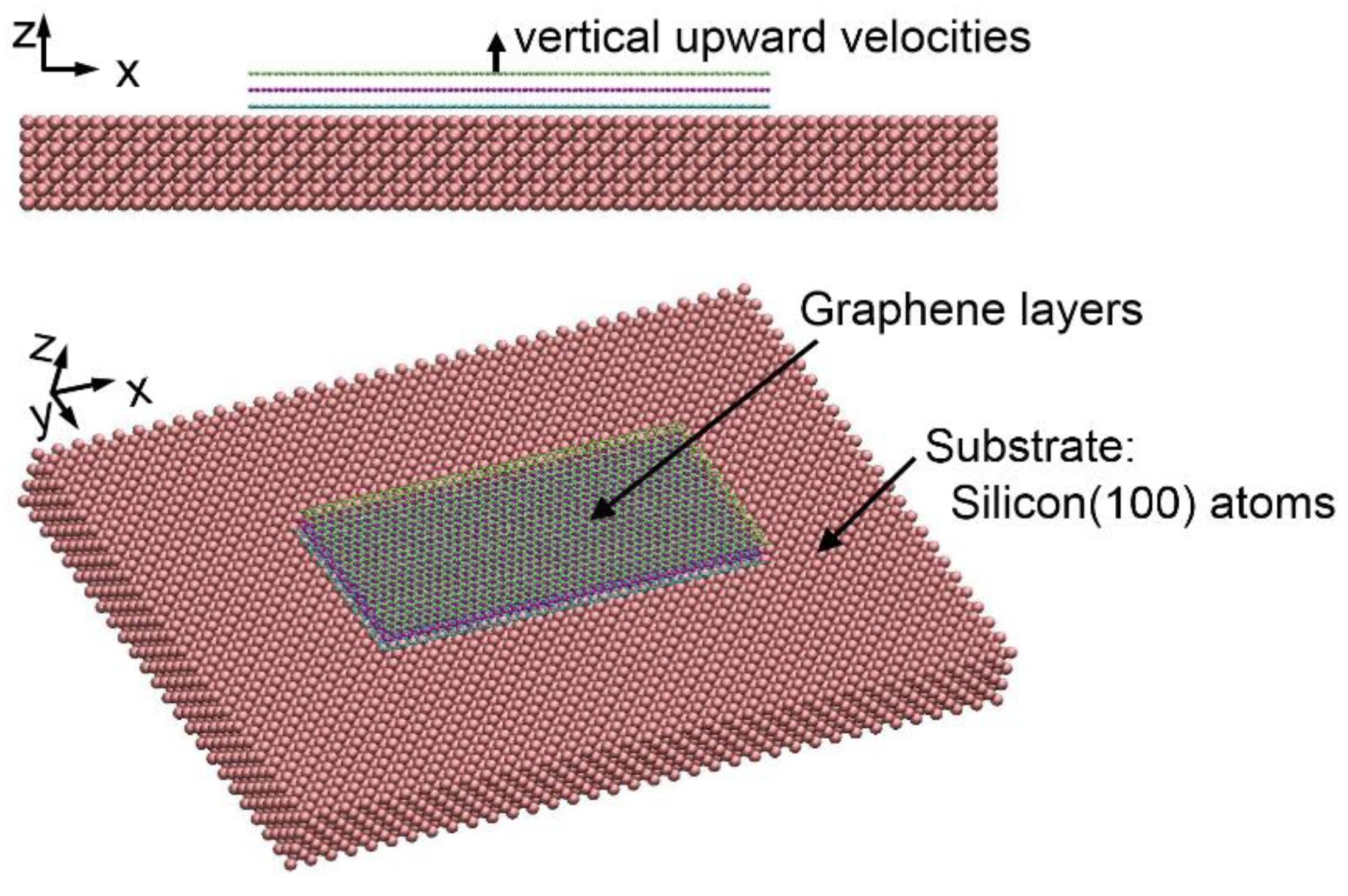
In this paper, the exfoliation process of one to ten layers of graphene from Si semiconductor substrates were simulated by the MD method, and the adhesion behavior between multilayer graphene and silicon substrates was studied. In order to simplify the model to exclude the interference of external factors (for example, factors, like friction, render the system much more complicated during sliding or wedge exfoliation, while errors may be introduced by fixed end during peeling or bubble exfoliation), we applied a series of external vertical upward velocities to the topmost layer to exfoliate graphene directly. The influences of the graphene layer number and exfoliation velocity on the bonding properties between graphene and silicon were clarified. In the system where graphene bonded to an Si semiconductor substrate, the bonding properties, critical velocities, adhesive forces, and adhesion energies were obtained. This research can promote further study of graphene-based MEMS/NEMS devices.
3. Results and Discussions
The exfoliation process of a three-layer system was studied and the results are discussed below. At first, a V
up of 5 Å/ps was applied to the topmost layer of graphene. Due to the force induced by the velocity, the topmost layer of graphene started to move up. The topmost graphene was also subjected to the force from the Si substrate and underlying layers of graphene. Because the velocity was too low to create enough force, the topmost graphene was pulled back to the substrate after reaching the farthest distance of 10.86 Å from the substrate surface at timestep 1422. In other words, if the external vertical constant velocity applied to the topmost layer is too low, the produced kinetic energy cannot exceed the adhesion energy, and thus graphene cannot move far away from the Si surface. This is similar to the experimental phenomenon in which a small speed excitation cannot produce any effective response. The external force created by the V
up was applied continuously to the topmost layer, and the distance between the topmost layer and the Si substrate surface peaked once again at timestep 5558. This peak value was 10.21 Å less than the first peak value, as shown in the black curve in
Figure 2a. Due to the constraint of the Si substrate and underlying layers, the external force created by the V
up was gradually balanced, and the topmost layer was located around 9.46 Å from the Si surface. From the displacement curve and graphene atomic trajectory shown in
Figure 2, it can be seen that the topmost layer cannot be exfoliated if the external V
up is 5 Å/ps.
Due to the van der Waals forces between the graphene layers, the three-layer graphene acted like a spring with a fixed bottom. The second and bottom layers of graphene moved up with the topmost layer at the beginning; their movement trends were in sync with the topmost layer and were almost identical. The second layer reached as far as 7.30 Å from the Si surface at timestep 1382, and the second peak was 6.70 Å at timestep 5743; meanwhile, the bottom layer reached only as far as 3.88 Å from the Si surface at timestep 1134, and the second peak occurred at timestep 5806 with a value of 3.25 Å. Like the topmost layer, the second layer and bottom layer were finally maintained at around 6 Å and 2.55 Å from the Si surface, respectively. According to the results shown in Figure 7, when the V
up was 5 Å/ps, the gap between the topmost layer and the second layer of graphene was no more than 3.87 Å. The largest gap occurred at timestep 170 when the topmost layer started to move up, and the gap varied slightly up and down. The external force and the internal interactions gradually reached a dynamic equilibrium, and finally the gaps between the topmost and second layers and between the second and bottom layers were stable at around 3.45 Å (as shown in Figures 7 and 8). The gaps were larger than the natural value of 3.35 Å. During the movements, the three graphene layers exhibited regular wavy fluctuations, and the fluctuation states of the three layers were consistent, as shown in
Figure 2b. It was found that, at a lower V
up, the three layers moved consistently because of the interlayer interactions of the graphene.
Once the V
up increased to 6.98 Å/ps, the external force induced by velocity was greater than the forces exerted by the Si substrate and underlying layers. The topmost layer of graphene was exfoliated, moving away from the Si surface gradually. The distance between the topmost layer and the Si surface increased with the timestep in a nonlinear fashion at the beginning. After timestep 2584, when the topmost layer of graphene was 13 Å away from the Si surface, the displacement curve (the black curve in
Figure 3a) became almost linear.
The second layer of graphene was forced upward with the topmost layer, since the pulling up force from the topmost layer of graphene was greater than the pulling down force from the Si substrate and bottom layer of graphene. The same condition occurred for the bottom layer, which moved upward together with the top two layers. At the beginning, the ascending rates of the three layers were different, leading to the maximum spacing of the topmost and second layers being 4.2 Å (shown in Figure 7), and the maximum spacing of the second and bottom layers being 3.92 Å (shown in Figure 8). After timestep 2584, when the effect of the substrate disappeared, the three layers went up at the same rate, and the three motion curves were parallel, as shown in
Figure 3a.
Figure 3b depicts one movement snapshot of the atomic trajectory. Because the interaction between graphene and the Si substrate was much more significant, the dislocation phenomena of Si surface atoms close to the edge of the graphene occurred. Graphene fluctuated wildly, but the atomic motion morphologies of the three layers were identical.
When a V
up of 9 Å/ps was applied to the topmost layer, the topmost layer of graphene could pull the second and bottom layers up, according to the observation of the atomic trajectories. The topmost layer completely eradicated the bandage of the Si substrate, and the three layers went up at the same rate after 1357 timesteps, when the distance between the topmost layer and the Si substrate was larger than 13 Å. A faster V
up created more momentum and caused the three layers to leave the Si surface more quickly, in addition to resulting in a larger maximum gap of 5.1 Å between the topmost and second layers (shown in Figure 7). The relative balance gap between the topmost and second layers was 3.44 Å larger than the natural graphene interlayer gap of 3.35 Å. From the atomic trajectories, shown in
Figure 4b, the three layers maintained consistent, huge waves.
With a V
up of 10.16 Å/ps, only the top can be unbound from the Si substrate and move far away from the underlying graphene and Si surface, as if the springs between the graphene layers were suddenly broken. Before timestep 2347, when the distance between the topmost layer and Si surface was less than 19.59 Å, the Si substrate and underlying layers still exerted forces on the topmost layer of graphene, and the movement curve of the topmost layer was nonlinear at the beginning, as shown in
Figure 5a. Once the distance between the topmost layer and the Si substrate was larger than 19.59 Å, the topmost layer could eliminate all constraints and move up linearly.
The second layer was pulled up by the topmost layer with a bulge at the centre, as a result of the strong interaction between the Si substrate and the edge of the graphene, which was caused by the unsaturated bonds of graphene edge atoms. The topmost layer attempted to pull the underlying layers up before 13,926 timesteps. However, after this time, the bulge slowly flattened. The red and blue curves in
Figure 5a show the displacement of the second and bottom layers of graphene, respectively, and the maximum average distance between the second layer and Si surface was 14.6 Å. Meanwhile, the maximum average distance between the bottom layer and Si surface was 10.9 Å. Finally, due to van der Waals forces from the Si substrate, the second and bottom layers were pulled back to the Si surface. During the central uplifting process of the underlying layers, the left and right edges of the second and bottom layers moved toward the center of the Si substrate, so that a more serious slip dislocation of Si surface atoms occurred (shown in
Figure 5b).
When the velocity was faster than 10.16 Å/ps—for example, 12 Å/ps—the displacement curve of three-layer graphene and the atomic trajectory were obtained as shown in
Figure 6. Graphene shed the constraints from the Si substrate and underlying layers much more quickly. Moreover, the second and the bottom layers were pulled up only a very short distance (with maximum distances of 7.03 Å and 3.5 Å, respectively) by the topmost layer at timestep 998, following with the tension of the topmost layer disappearing, and the underlying two layers were balanced at 6.11 Å and 2.69 Å, respectively, on the Si surface.
It can be seen from
Figure 7 and
Figure 8 that, when the V
up was 6.98 Å/ps or 9 Å/ps, the topmost layer of graphene pulled the second and the bottom layers up, and all three layers were able to separate from the Si substrate together. When the velocity was 10.16 Å/ps or 12 Å/ps, the topmost layer was exfoliated alone. By massive calculations, it can be concluded that, if the V
up is less than 6.98 Å/ps, graphene cannot be exfoliated; if the V
up is in the range of 6.98 Å /ps–10.16 Å/ps, three-layer graphene can be exfoliated entirely; if the V
up is faster than 10.16 Å/ps, only the topmost layer can be exfoliated. As a result, velocities of 6.98 Å/ps and 10.16 Å/ps were determined to be the critical exfoliation velocities for three-layer graphene systems.
Figure 9 summarizes the Z direction forces of all three layers of graphene at 5 Å/ps, the first critical V
up of 6.98 Å/ps, 9 Å/ps and the second critical V
up of 10.16 Å/ps.
Figure 10,
Figure 11 and
Figure 12 show the Fz of the upmost layer, the second layer, and the bottom layer of graphene at 5 Å/ps, the first critical V
up of 6.98 Å/ps, and the second critical V
up of 10.16 Å/ps, respectively. The initial distance between the Si surface and the bottom layer of graphene was small and there was a repulsive force, so the external Fz was a negative value that was reduced with timestep. At timestep 238, the spacing between the graphene bottom and the substrate was 2.6 Å, and the interaction between the graphene and substrate reached 0 nN. At timestep 417, the force exerted on all three layers reached 23.96 nN. In the process of balancing the external forces and the internal forces, the Fz fluctuated violently and erratically until timestep 2800, after which the fluctuation amplitude of the force was somewhat stable. Following the changes of the distance between the upmost layer of graphene and the Si surface, the Fz fluctuated between −26 nN and 20 nN, with a trend of decreasing amplitude. In comparison, the Z direction forces on the second layer of graphene were more complex, and the force curve was more disordered.
At 6.98 Å/ps, according to the displacement and motion trajectory, the top layer of graphene was exfoliated together with the underlying two layers. At timestep 403, the maximum Fz of all three layers was 26.73 nN. At this time, the distance between the bottom layer of graphene and the Si surface was 3.13 Å. When the three layers were exfoliated entirely, at about timestep 2800, the force gradually reduced to zero. Meanwhile, the bottom layer was 6.16 Å from the Si surface. The Fz of all three layers on each layer of graphene fluctuated violently at the beginning. The Fz variation of the bottom layer started to become harmonic at timestep 3200, and the amplitude range was between −33 nN and 45 nN. The top graphene started the harmonic change at 3700 with an amplitude of −42 nN–35 nN. The Fz curve of the second layer of graphene was more disordered.
When the Vup exceeded the first critical of Vup 6.98 Å/ps, the variation curve of the Fz applied to the three-layer graphene system over time was relatively smooth at 9 Å/ps. At timestep 434, the maximum force was 23.67 nN. After plenty of calculations, it was found that when the top layer of graphene was between 6.98 Å/ps and 10.16 Å/ps, the strongest force for stripping off the three layers of graphene was 26.73 nN, representing the adhesion force required for the exfoliation of all three layers of graphene.
Only the topmost layer of graphene was exfoliated at the critical V
up of 10.16 Å/ps, so the force of the three-layer graphene as a whole cannot be counted. As can be seen from
Figure 10, at timestep 64, the topmost layer was subjected to the maximum force of 74.75 nN, and this was the adhesion force required for the exfoliation of the topmost layer of graphene. The Fz of the topmost layer of graphene was almost zero after timestep 1500, when it moved to a distance of 16.78 Å away from the Si surface. When the topmost layer was completely exfoliated, the Fz forces applied to the second and bottom layers of graphene gradually decreased to zero.
In order to obtain the adhesion energy between graphene and the Si substrate, the work done (W) by Fz was calculated, which was defined as the direction force (Fz) applied to graphene multiplied by the average distance the graphene layer moved (S):
The work done by the external force to all three layers was negative before timestep 234 (shown in
Figure 13). This is because when the three-layer graphene was exfoliated entirely at a velocity of 6.98 Å/ps, the effect of the negative direction of the Fz on all graphene layers was caused by the existence of the repulsive force between graphene and the Si surface. Under the critical V
up of 6.98 Å/ps, the work curve of the Fz showed a certain fluctuation due to the variations of the external force, and finally was reduced to zero due to the disappearance of the external force. The maximum work done to exfoliate the three layers was 68.51 mJ/m
2, which was equal to the adhesive energy of the entire three-layer graphene. When the critical velocity was 10.16 Å/ps, only the topmost layer was exfoliated, and the work curve of the topmost layer by the external force is shown in
Figure 14. The maximum work value of the external force was 148.31 mJ/m
2, which was equal to the adhesive energy of the topmost layer in the three-layer graphene system.
The exfoliation processes of one- to ten-layer graphene systems were calculated. Additionally, the critical velocities, the maximum exfoliation forces, and the adhesion energies were calculated and are summarized in
Figure 15,
Figure 16 and
Figure 17, respectively. Once the number of graphene layers exceeds three, the total number of graphene layers cannot be exfoliated together; only the topmost layer can be freed. For one layer of graphene, the critical V
up was 4.3 Å/ps. In a two-layer graphene system, the critical values of V
up to exfoliate both layers and only the topmost layer were 5.2 Å/ps and 12 Å/ps, respectively. In a three-layer graphene system, the critical V
up to exfoliate all three layers increased to 6.98 Å/ps, and the critical exfoliation velocity of the topmost layer was 12 Å/ps. The critical exfoliation V
up values for four layers to ten layers of graphene were in the range of 10 Å/ps–12 Å/ps. If the number of graphene layers was less than three, all graphene layers could be exfoliated together if the V
up was in the range between the two critical exfoliation velocities. So, we propose a new bonding mechanism according to the different numbers of graphene layers: In a system where the number of graphene layers is two or three, there are two critical exfoliation velocities. Graphene cannot be exfoliated when the velocity is less than the first critical V
up; all graphene layers can be exfoliated together when the V
up is in the range between the two critical velocities; and only the topmost layer can be freed from the Si surface if the velocity is greater than the second critical V
up. In systems where the graphene layer number is four to ten, only the topmost layer can be exfoliated if the V
up is high enough. This means that, for two-layer or three-layer graphene systems, it is not the case that a faster exfoliation velocity will make it easier to exfoliate graphene. If the applied external velocity is in the range between the first and second critical velocities, a relatively low velocity can be used to peel all of the graphene. If the velocity is higher than the second critical V
up, only the topmost layer can be exfoliated, no matter the magnitude of the V
up. The adhesion force needed to exfoliate the topmost layer of graphene is minimal in a monolayer graphene system, with a value of 25.04 nN. This is because monolayer graphene is only subjected to the force from the Si substrate. The maximum adhesion force of 74.75 nN to exfoliate the topmost layer occurred in a three-layer graphene system, due to the maximization of the resultant forces from the Si substrate and underlying layers. If the graphene layer number is more than three, the adhesion force decreases with the increasing graphene layer number. The reason for this is mainly that the distance between the topmost layer and Si substrate increases with increasing layer numbers, so the interaction of the Si substrate with the topmost layer is decreased. Therefore, the adhesion forces needed to exfoliate the topmost layer in one-layer to ten-layer graphene systems are in the range of 25.04 nN–74.75 nN. From
Figure 17, it can be seen that the adhesion energies needed to exfoliate the topmost layer in one-layer to ten-layer graphene systems are in the range of 73.5 mJ/m
2–188.45 mJ/m
2, which is consistent with the results in the literature [
11].
Whether the adhesion between graphene and semiconductor substrates is firm or not will affect the yield, life, and performance of graphene-based MEMS/NEMS devices. This was deeply felt when we were fabricating a graphene-based MEMS device. In contrast, when we were fabricating traditional silicon MEMS sensors, the silicon piezoresistor was N/P-doped in the silicon substrate. Thus, the sensitive resistance bar and the substrate were all one, and it was not necessary to consider the bonding mechanism between the silicon sensitive resistance bars and the silicon substrate. However, in graphene-based MEMS devices, graphene membranes are usually attached to the silicon substrate surface by the transferring method from copper. The graphene-substrate interaction is characterized by weak physical van der Waals forces. For this reason, the adhesion behavior was studied in this paper by molecular dynamics. The adhesion energy (73.5 mJ/m2–188.45 mJ/m2) between graphene and the Si substrate indicated the reliable bond strength. Otherwise, without the oxygen plasma treatment process, the cleaning technologies, and the drying process in an ultra-clean room, the influence of surface roughness, trapped charge, and trapped molecules, including H2O on the bonding strength, needs to be studied. We will try to do further research focused on this theme. We will also try to prepare the relative experiment, although it is difficult to reproduce the simulation model by experiment. We hope to provide experiment results in the future according to the similarity criterion of the physical model.
