Abstract
Aiming at improving the performance of the existing for single-phase electric springs (ESs), such as the fastness of the voltage stabilization and the mitigation of the voltage harmonics across the critical loads (CLs), the dead-beat control cooperating with state observer is proposed in this paper. First, the δ control is reviewed, outlining its features of regulation of the CL voltage while keeping the ES operation stable. After describing the operation of an ES in the continuous-time domain by the state-space technique, its discrete-time model is formulated using the zero-order-hold (ZOH) algorithm. Then, the control system for an ES is designed around the dead-beat control cooperating with a state observer and implementing the two typical compensation functions achievable with the δ control, namely the pure reactive power compensation and the power factor correction. Results obtained by simulation demonstrate that the control system is able to both properly drive an ES and to implement the two functions. The results also show that the proposed control system has the advantage of eliminating harmonic components in CL voltage when grid voltage distorts.
1. Introduction
Electric springs (ESs) have been proposed five years ago as a new solution to fully exploit the unpredictable power generated from intermittent renewable energy sources (RESs) [1]. Compared to the traditional operating way of the power system, they carry out the paradigm that load demand matches power generation automatically [2,3]. From the topology point of view, an ES is built up by connecting a circuit which behaves like a voltage source inverter (VSI), in series to the non-critical loads (NCLs) of a user with the purpose of keeping constant the magnitude of the voltage across its critical loads (CLs). Consequently, the control approaches for VSI have been initially introduced to drive the ES systems [4,5]. Subsequently, the control approaches for power converters [6,7] and microgrids [8,9] have been adopted. With the increasing power generation from RESs [10], the ESs have gained an increasing interest and many papers have appeared, reporting on system modeling [11], reactive power compensation [2], power decoupling [12,13], voltage and frequency control [14], power balance control for a three-phase system [15], and so on.
Among the compensation functions that the control of an ES can implement, the pure reactive power compensation is the key one because it stabilizes the voltage across the CLs without exchanging (absorbing or delivering) active power. The basic control of an ES implementing such compensation was reported together with the ES concept in Reference [1]. After that, the δ control was proposed in Reference [2]; it imposes the instantaneous phase angle δ by which the CL voltage lags the line voltage to ensure that ES does not exchange any active power at the steady state. Once calculated the angle δ, the control scheme uses a proportional resonant (PR) controller for the outer-loop regulation of the CL voltage and a proportional (P) controller for the inner-loop adjustment of the ES current. This setup of the δ control exhibits some shortcomings. For instance, its application requires the design and tuning of the three parameters of the PR and P controllers. Another shortcoming is that the PR controller is not suitable for nonlinear systems so that the CL voltage may be severely distorted when the line voltage is affected by harmonics. What is more, system modeling in [2] is not enough accurate since the line voltage is regarded as a disturbance which results in unexpected dynamic performance. Considering the benefits of the δ control and side effects of the PR controller, the goal of this paper is to find out a more practical controller that facilitates the application of the δ control and, at the same time, improves the performance of the existing setup.
The dead-beat control uses the discrete-time model of a system to predict the amplitude of the controlled variable one or more sampling times in advance. By forcing this amplitude to track that one of the reference, the error between the controlled variable and the reference is zeroed [16]. The characteristics of the relevant controller are the low complexity and a high-performance system [17]. Therefore, it is utilized as the control tool that allows the achievement of the goal of this paper.
As explained in Reference [2], an ES is a multi-input and multi-output system where only two control objectives can be achieved at the same time. The main objective is the regulation of the CL voltage that is expected to have a sinusoidal shape with a preset magnitude. The other objective cis to implement a specific compensation function by imposing the phase angle δ. In this paper, the two most significant functions, i.e., the pure reactive power compensation and the power factor correction (PFC), are chosen as objective. The effectiveness of the resulting control system is highlighted by comparing its performance to that obtained with the existing PR and P controllers.
In detail, this paper is organized as follows. In Section 2, the operating principle of a single-phase ES driven by the δ control is introduced. In Section 3, system modeling and design of the dead-beat controller are provided; the design of a state observer to reduce the control period of the dead-beat control is also given. In Section 4, two controllers based on the same δ control, one using the dead-beat control cooperating with state observer and the other one using the PR and P controllers, are investigated by simulation under implementation of both the compensation functions. The simulation results reveal the better performance attained by the proposed controller such as the fast dynamics and the harmonic suppression. Finally, the conclusions are drawn in Section 5.
2. Operating Principle of Single-Phase ESs
2.1. The Topology of Single-Phase ES
The typical topology of a single-phase ES embedded in a power system is shown in Figure 1. In the figure, the ES is drawn within the dashed line, box, and consists of a current-controlled single-phase VSI that impresses the voltage vES across capacitor C with help from the inductance L. Moreover, in the figure, Z2 is the CL with limited operating voltage range and Z3 is the NCL with wide operating voltage range; the series of the ES and Z3 constitutes the so-called smart load (SL) and is connected in parallel with Z2, where the point of common coupling is designated with point of common coupling (PCC). Other variables in the figure are the voltages across Z2 and Z3, denoted with vS and vNC, the output voltage of the VSI, denoted with vi, the currents through Z3 and the line, denoted with i3 and i1, respectively, and the output current of the ES, denoted with iL. Variable vG represents the voltage at the injection point of RES, whereas R1 and L1 are the line resistance and inductance. Vector subtraction of vG from the voltage drop across the line impedance gives vS.
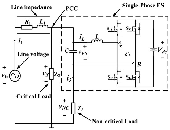
Figure 1.
The typical topology of a single-phase ES embedded in a power system. ES: electric springs; PCC: point of common coupling.
As explained in Reference [1], the ES is an electrical circuitry that generates an ac voltage intended to regulate the CL voltage while passing the voltage fluctuations of the RESs to the NCLs.
2.2. δ Control of Single-Phase ES
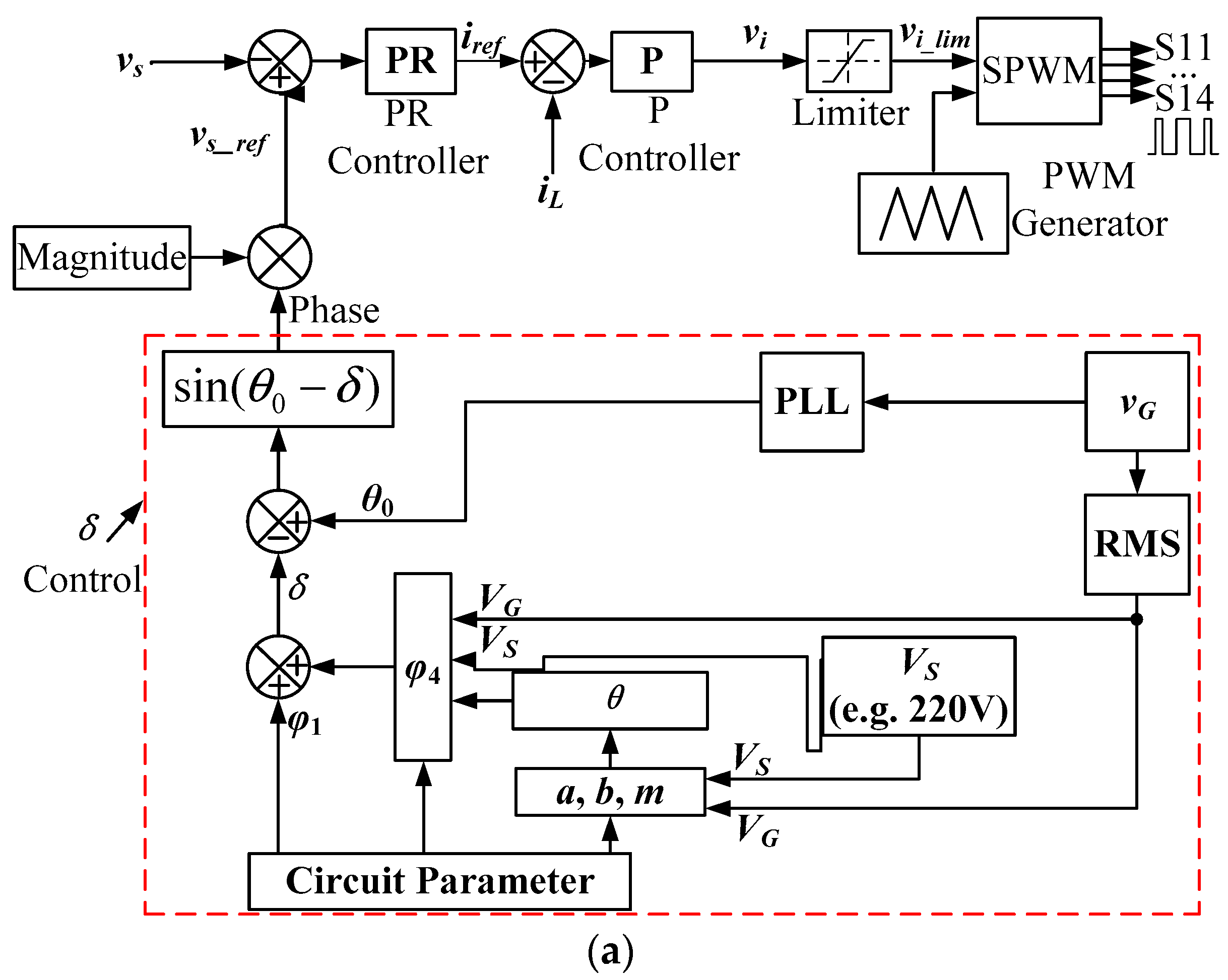
The scheme of the existing setup of the δ control for a single-phase ES is depicted in Figure 2a. In the figure, a double loop control is arranged with a PR controller in the outer CL voltage loop and a P controller in the inner ES current loop. The purpose of the δ control is to impose the phase lag of vS with respect to vG. The calculation of δ is based on the vector diagram of the circuit in Figure 1 and is executed for the ES to implement a certain compensation function.
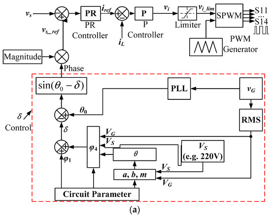

Figure 2.
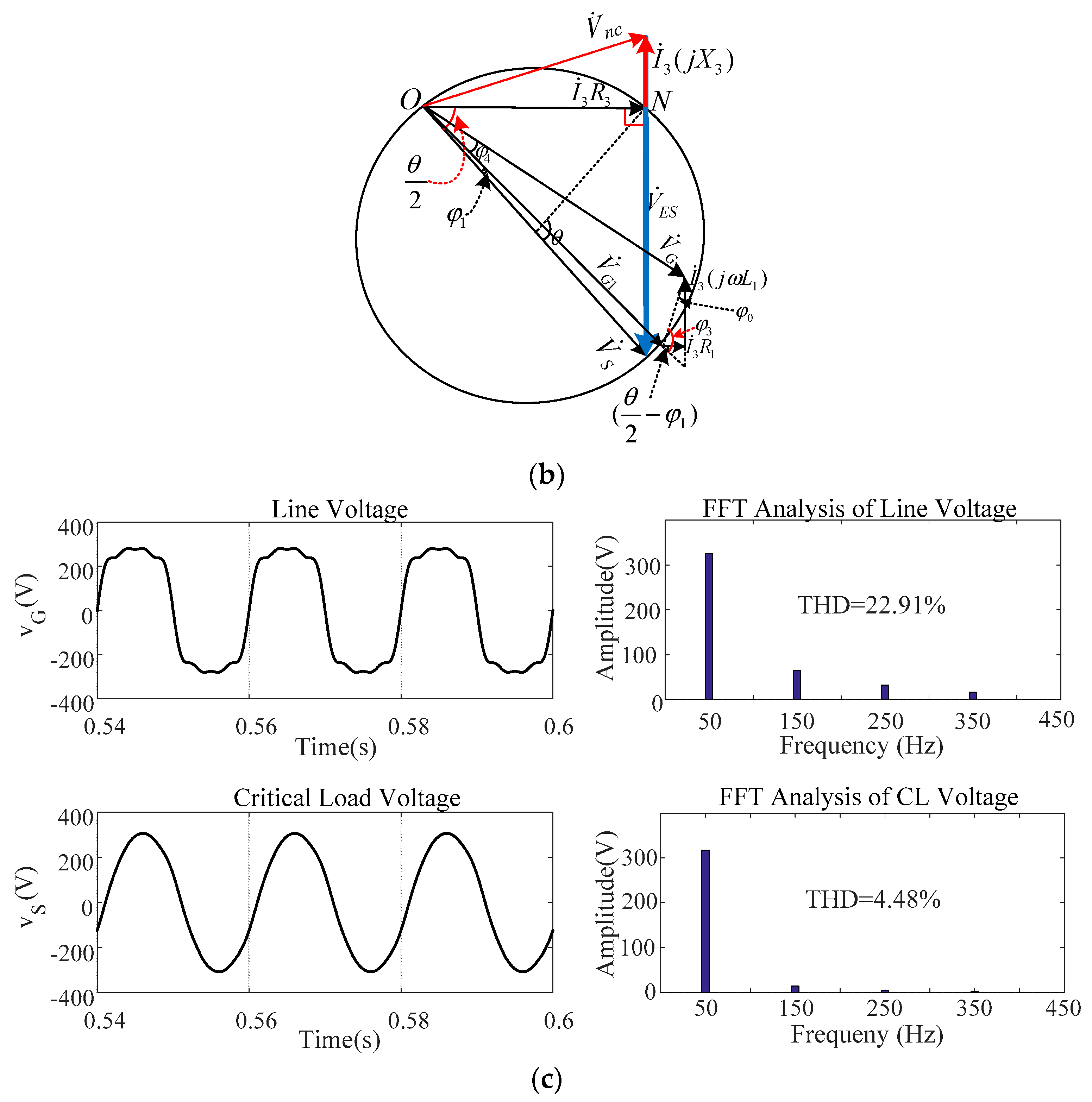
The existing δ control setup of the single-phase ES. (a) Control scheme. (b) Vector diagram of the δ control in the capacitive mode as an example. (c) Fast Fourier Transformation (FFT) analysis of grid voltage and critical loads (CL) voltage under distorted conditions. PR: proportional resonant; THD: total harmonic distortion; SPMW: sinusoidal pulse width modulation; RMS: root mean square.
The details of the control scheme in Figure 2a are as follows. Signal vS_ref is the sinusoidal reference of voltage for vS. Its magnitude is fixed by the user while its phase angle lags that of vG of δ. The error between vS and vS_ref is fed into the PR controller to generate the reference signal iref for the ES of current. In turn, the error between the actual ES current iL and iref is fed into the P controller to generate, via a limiter, the signal v_comp for the pulse width modulation (PWM) generator. The latter one delivers the four commands for the VSI switches. It is a matter of fact that the calculation of δ, schematized within the dashed line box in Figure 2a, depends on the compensation function to be achieved and, accordingly, determines the voltage reference signal As explained in Reference [2], θ0 denotes the phase of the grid; φ1 is the impedance angle of line impedance; a,b and m denotes the coefficients to calculate φ4; Besides, θ and φ3 are the complementary results during the δ calculation.
Figure 2b shows the vector diagram of the power system in Figure 1 when ES operates in the so-called capacitive mode which occurs when the CL voltage is lower than its rated value. Details on the δ calculation can be found in Reference [2]. The inductive mode can be explained in a similar way. It is worth to remark that the δ control assumes that the length of transmission line is known in order to get acquainted of the line resistance and inductance since their values are necessary to calculate δ; the way to derive the line impedance can be found in Reference [1].
2.3. Issues in the δ Control with PR and P Controllers
A single-phase ES is satisfactorily controlled by the existing setup of the δ control under ideal grid conditions. However, when vG is distorted to some extent, the total harmonic distortion (THD) of the CL voltage can be somewhat high and, sometimes, is out of the specifications. Although the THD value can be enhanced by properly tuning the parameters of the PR and P controllers, there are still limitations in the real application. For instance, it is convenient that the parameter kp of the PR controller does not exceed 3. Referring to the study case reported below, when the parameters kp and kr of the PR controller are selected as 2 and 20, and the gain of the P controller is selected as 0.5, the THD value of the CL voltage is up to 4.48% for a THD value of vG of 22.9%, as pointed out in Figure 2c. This calls for an improvement of the performance of an ES by developing a different solution for the setup of the δ control.
3. Dead-Beat Control for Single-Phase ESs
3.1. System Modeling of Single-Phase ES
As explained in Reference [11], by neglecting the dynamics of the ES DC bus, the equations of an ES are linear and time-invariant as explicated hereafter to simplify the ES modeling, both CL and NCL are taken of resistive type.
Applying Kirchhoff’s Voltage Law (KVL) yields
Solving Equations (1)–(4) yields
Solving Equations (5)–(7) yields
Based on the equations above, the state-space model of the ES can be written as follows:
where,
3.2. Dead-Beat Control for Single-Phase ES
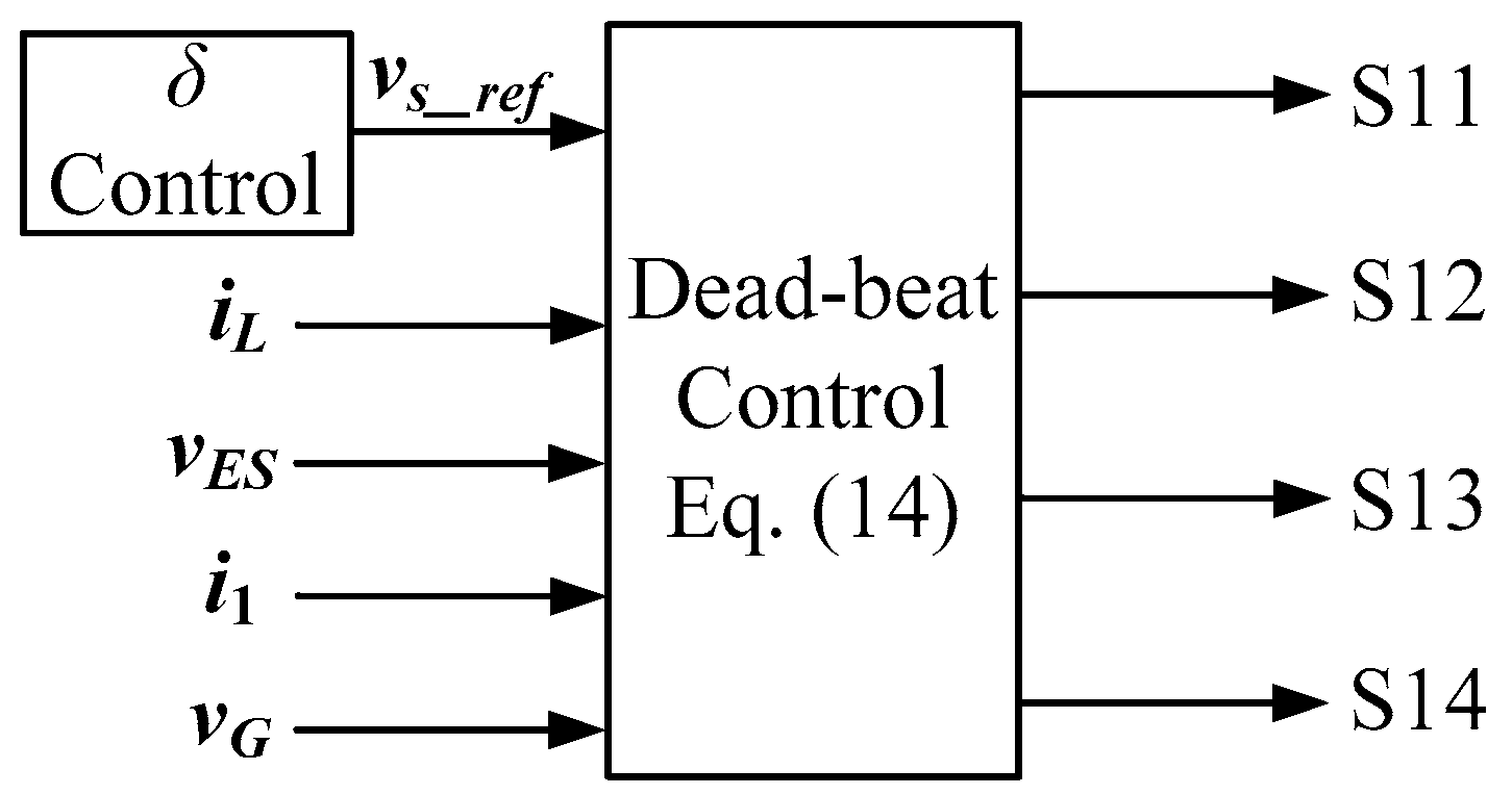
The control system proposed in this paper is still based on the δ control but replaces the PR and P controllers with a dead-beat controller. The scheme of the control system is drawn in Figure 3; its effectiveness, as well the comparison of its performance with that of the existing setup, are presented in the next sections.
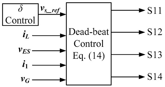
Figure 3.
The proposed dead-beat control based on the δ control.
The operating principle of a dead-beat controller is illustrated in Reference [16]. Since here the dead-beat control is applied for the first time to an ES, the design of the relevant controller is exposed step-by-step.
The first step is to discretize Equation (9). By using the zero-order-hold (ZOH) algorithm, the discrete-time state space model of Equation (9) can be expressed as
where, x(k) = [iL(k) vES(k) i1(k)]T, u(k) = [vG(k) vi(k)]T, and
The system output at of the next control period is
where, G = C*A = [a1 a2 a3] and H = C*B = [b1 b2]. By making y(k + 1) equal to the reference value at the next control period, designated as r(k + 1), it follows that:
Equation (12) holds on condition that the system is entered with a suitable value of the input vi(k). Let this condition be satisfied. Equation (12) outlines that the output of the controlled system equates the reference value at each control period, which means that the tracking error of the control system is zero.
Substituting the respective coefficients into Equation (12) yields
Solving Equation (13) gives the required input
The working equation of the dead-beat controller is given by Equation (14). vi(k) is calculated, it is made to enter the PWM generator at each control period. Note that r(k + 1) in Equation (14), which is defined as vS_ref in Figure 3, is calculated by the δ control.
3.3. Dead-Beat Control Cooperating with State Observer for Single-Phase ES
The execution of the dead-beat control could be quite demanding, to avoid the shortcoming of significantly increasing the maximum width of the voltage pulses at the VSI output, it is convenient to, calculate vi(k) s one control period ahead. This implies that vi(k) must be calculated in the (k − 1) control period by resorting to an estimation of the associated variables. A good tool to estimate the variables of a system is a state observer [18], as shown in Figure 4a,b. Here, a full order observer is used, expressed as
where, H is the observer gain matrix. The error vector of the state observer is
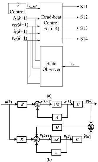
Figure 4.
The proposed dead-beat control cooperating with state observer. (a) Full control diagram; (b) Diagram of the state observer adopted in the control.
The dynamic properties of the error vector depend on the eigenvalues of the matrix (A − HC). For a stable (A − HC), the error vector tends to zero for any initial error vector e(0). In other words, will converge to x(k) regardless of the values of x(0) and .
If the control system is completely observable, it can be proven that H can be chosen in order that (A − HC) is asymptotically stable and has the desired dynamics o that the error vector moves toward zero (origin) at a speed fast enough. This outcome is achieved by a suitable placement of the eigenvalues of (A-HC). In practice, the poles of the observer are placed within three to five times far away from the imaginary axis than the poles of the control system.
4. Simulation and Discussions
To test the arranged control system, simulations are conducted under the environment of Matlab/Simulink for the study case of an ES with the data reported in Table 1. Both the T compensation functions mentioned above, i.e., the pure reactive power compensation and the PFC, have been implemented in the control system for a thorough evaluation of its performance.

Table 1.
The study case data. SL: smart load; ES: Electric springs; CL: critical load; NCL: non-critical load; DC: direct current.
The control specifications are (1) the CL voltage sis regulated to 110 V; (2) for the pure reactive power compensation, the phase angle between ES current and ES voltage is 90°; for PFC, the voltage vG is in phase with the line current.
4.1. Flowchart of Dead-Beat Control for δ Control
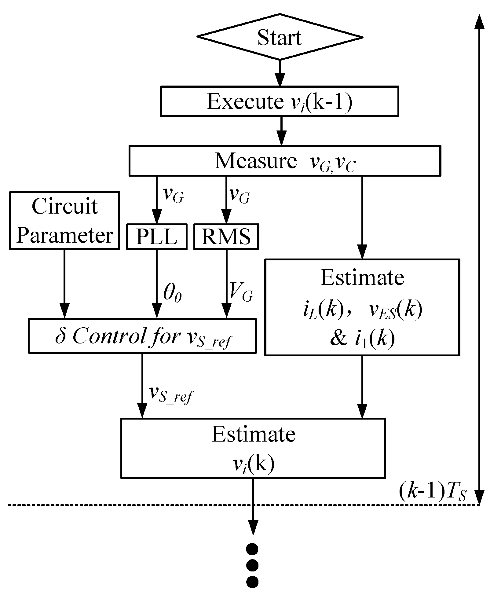
In the block of Matlab function, the program flowchart for dead-beat control and δ control is depicted as shown in Figure 5 which can be summarized as follows.
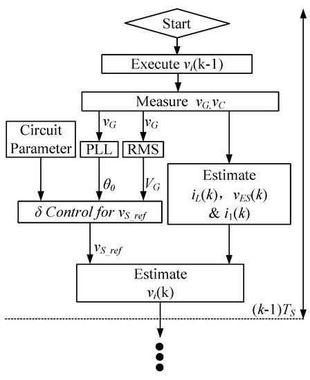
Figure 5.
The program flowchart of dead-beat control and δ control.
- Execute vi(k − 1) to the VSI within single-phase ES
- Measure grid voltage vG and PCC voltage vC
- Predict grid current i(k), inductor current iL(k), and capacitor grid vES(k)
- Calculate the reference of CL voltage based on the detected instantaneous phase and RMS value of grid voltage, and also based on circuit parameters
- Calculate the modulation signal vi(k)
4.2. Pure Reactive Power Compensation Mode
In this part, the simulations are divided into two steps, of which the one is under ideal grid conditions and the other one is with grid distortions.
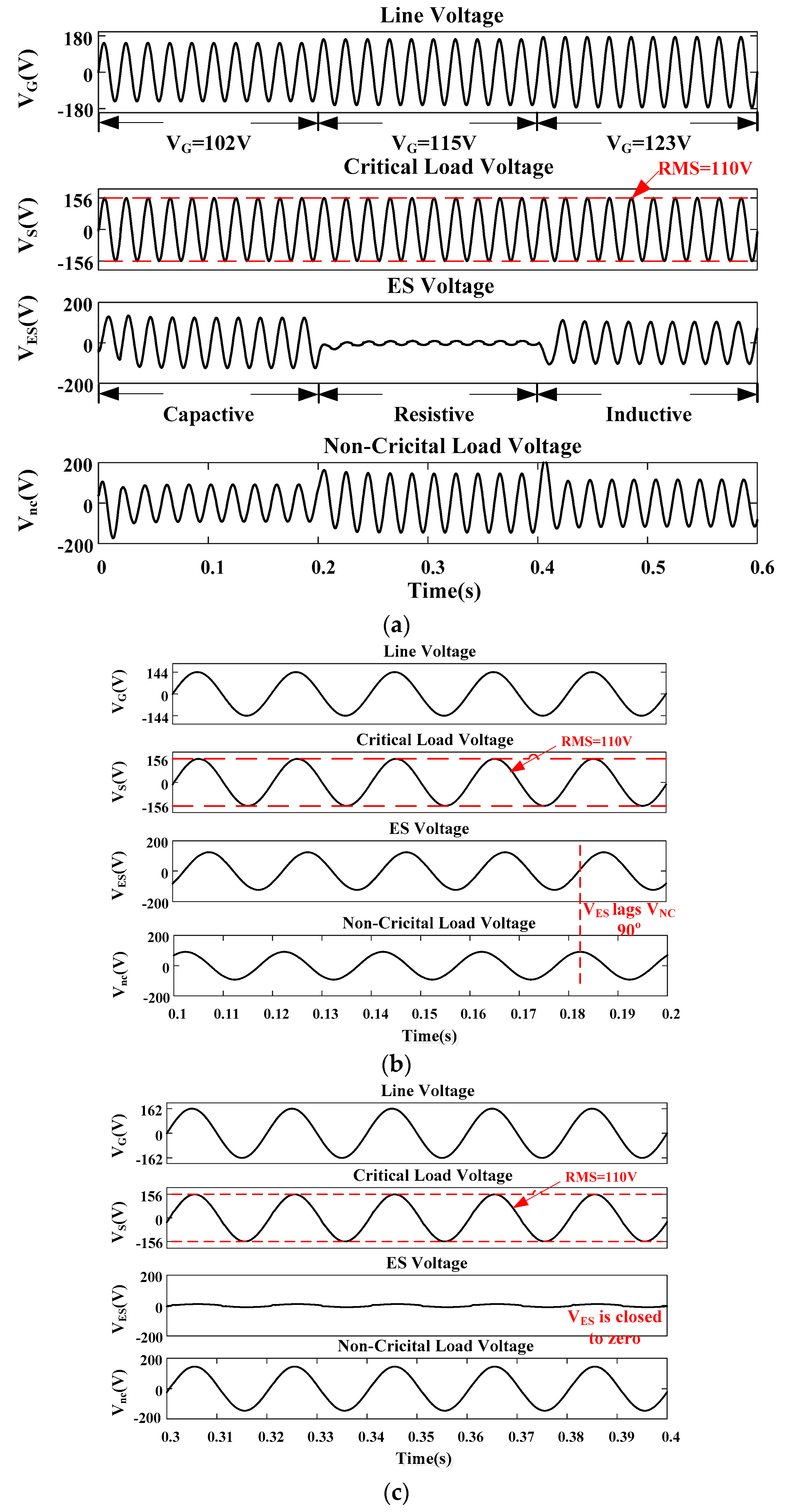
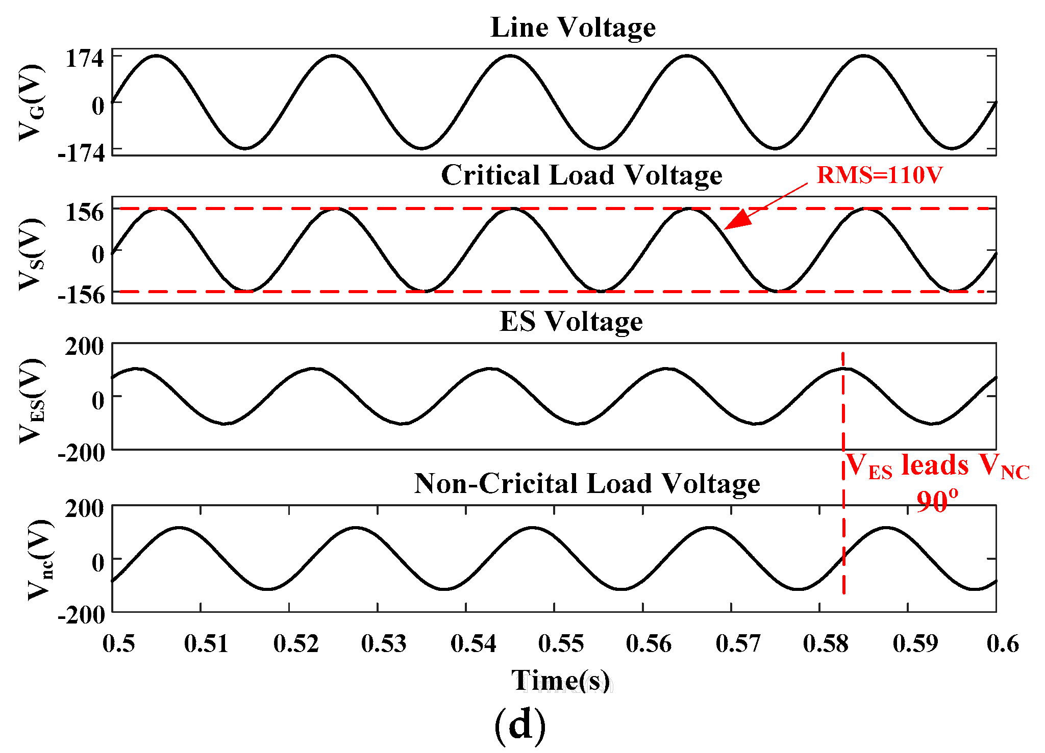
(1) Ideal Grid Conditions: The parameters for simulation are the same as Table 1 and there is no distortion on the line voltage. Figure 6 shows simulation waveforms under ideal grid conditions when dead-beat and δ control are both applied to the single-phase ES. As explained in Reference [6], three typical values such as 102 V, 115 V, and 123 V are selected to simulate capacitive mode, resistive mode, and inductive mode, respectively. In each subfigure, four channels are recorded as line voltage, CL voltage, ES voltage, and NCL voltage, respectively. Figure 6a is the overview all the full time ranges including three different modes. In Figure 6b when VG is set to 102 V, ES current which is in phase with NCL voltage leads ES voltage by 90°, which can be observed at 0.1832 s, meaning that the ES operates at the capacitive mode; In Figure 6b when VG is set to 115 V, ES voltage is very low and NCL voltage is almost the same as the CL voltage, meaning that the ES operates at the resistive mode; In Figure 6c when VG is set to 123 V, ES current lags ES voltage by 90° at 0.5873 s, meaning that the ES operates at the inductive mode. It can also be observed from Figure 6b–d that CL voltages are well regulated to be sinusoidal and RMS values are almost around 110 V. It is validated from the results above that the two control objectives under the pure reactive power compensation mode and also under ideal grid conditions have been achieved with the proposed dead-beat and δ control.


Figure 6.
The simulation waveforms based on the dead-beat and δ control under the ideal grid conditions and pure reactive power compensation mode. (a) Three operating modes at full time ranges; (b) Capacitive mode @VG = 102 V; (c) Resistive mode @ VG =115 V; (d) Inductive mode @ VG = 123 V.
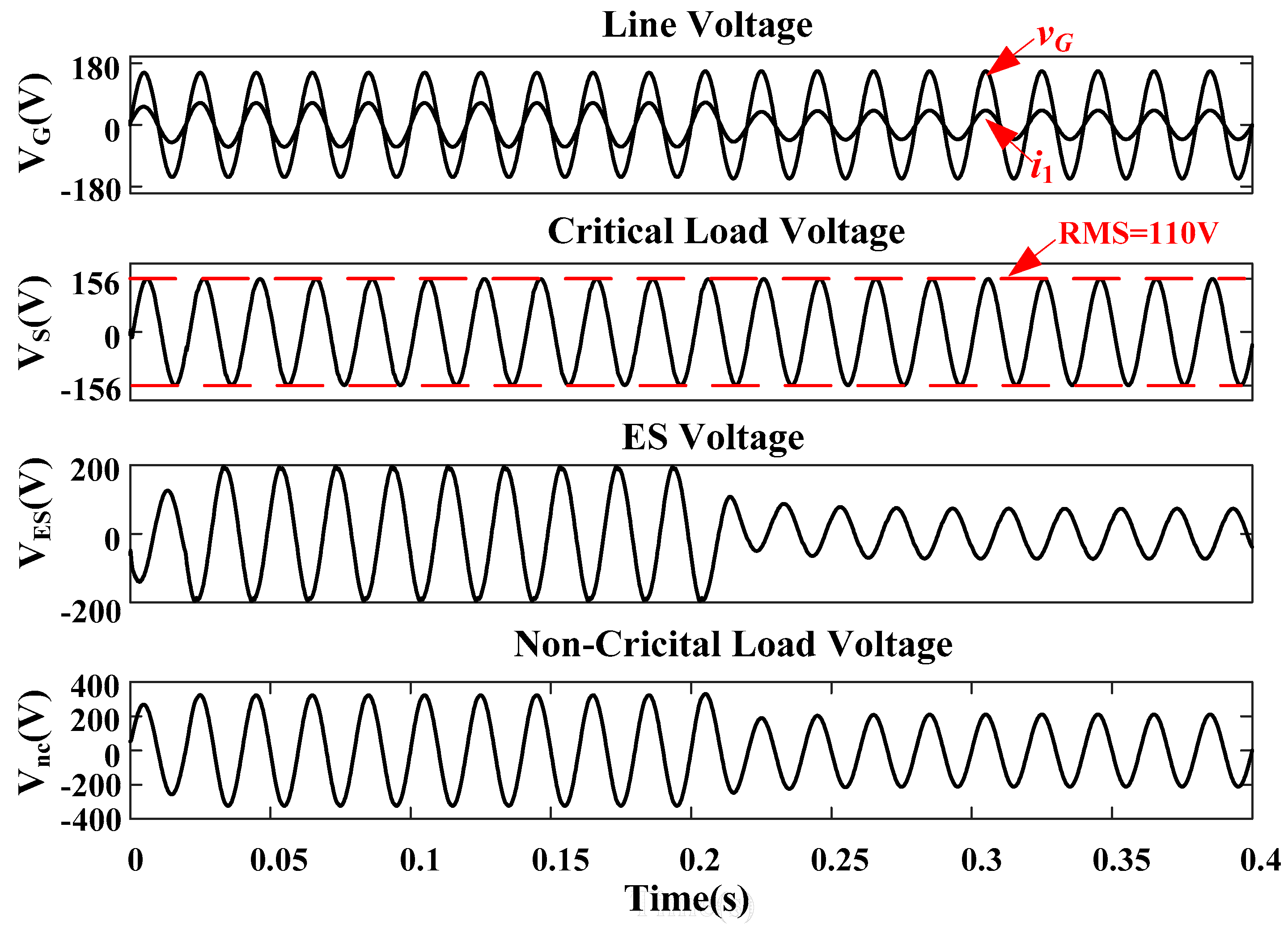
(2) Grid Voltage Distorted: The parameters for simulation are the same as Table 1. The only difference is that the grid voltage is set as follows. From 0 to 0.3 s, the nominal value of VG is set to 102 V without any distortion. From 0.3 s to 0.6 s, the 3rd, 5th, and 7th harmonic components are added to the fundamental element, of which the amplitudes are 20 V, 10 V, 5 V, respectively.
As a result, the THD value of vG is up to 22.46%, which is the same as that in Figure 2c. Figure 7a shows the simulation waveforms before and after grid distortion. Before 0.2 s, the ES operates at the capacitive mode and both ES voltage and CL voltage are sinusoidal. However, after 0.3 s, it is seen that the distortion on the line voltage has been passed to NCL voltage by the ES. It can also be seen that CL voltages are regulated well during the full time range. Figure 7b shows that the THD value of CL voltage is controlled to 1.54%, which is far smaller than that with the PR and P controllers. It should be noticed that when the grid voltage is distorted, the rms value of its fundamental component is used for δ calculation. If the δ is not accurate, the rms value of the PCC voltage will not be affected, only the ES will deviate a little bit from the pure reactive power compensation mode.
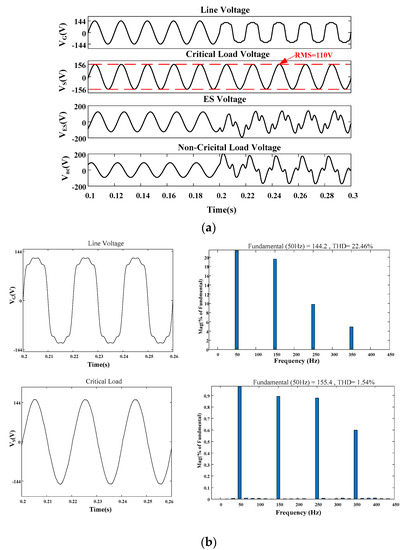
Figure 7.
The simulation waveforms based on the dead-beat with observer and δ control under the pure reactive power compensation mode. (a) Comparison between ideal grid condition and distorted condition; (b) FFT analysis of line voltage and critical load voltage under distorted grid condition.
4.3. PFC Mode
The purpose of this part is to double check the performance of the proposed dead-beat control cooperating with observer and δ control. Parameters are the same as Table 1 and the flowchart is also the same as Figure 5. The difference between the PFC mode and pure reactive power compensation mode is the codes for δ calculation, which is explained in Reference [2] in detail. The simulation is divided into two time intervals. In the first time interval which is from 0 to 0.2 s, VG is set to 108 V. In the second time interval from 0.2 s to 0.4 s, VG is set to 112 V. The simulation results are shown in Figure 8, where four channels are recorded. Line voltage and line current are recorded together in the first channel to show the effectiveness of PFC.
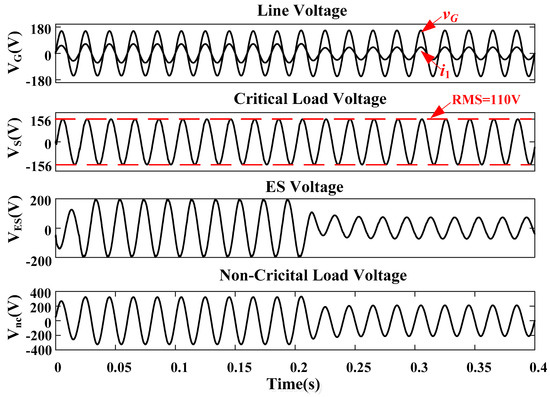
Figure 8.
The simulation waveforms based on dead-beat and δ control under the power factor correction (PFC) mode.
In Figure 8, it is obviously seen that zero crossing points in the first channel are the same and also in the same direction, which means that line current is controlled in phase with that of line voltage, even if VG changes. CL voltage in the second channel is controlled at 110 V. ES voltage and NCL voltage are recorded in the third and fourth channels, respectively. It is noticed that the phase angle between ES voltage and ES current are not strictly 90°. For instance, at 0.105 s when VG is 108 V, ES current which is in phase with NCL voltage, leads ES voltage for more than 90°, meaning that ES provides some active power. At 0.365 s when VG is 112 V, ES current leads ES voltage by less than 90°, meaning that ES absorb some active power. The reason is that only two control objectives can be achieved at the same time, of which one is the CL voltage and another one is the PFC function.
The effectiveness of the proposed dead-beat and δ control has been validated by the simulations results above.
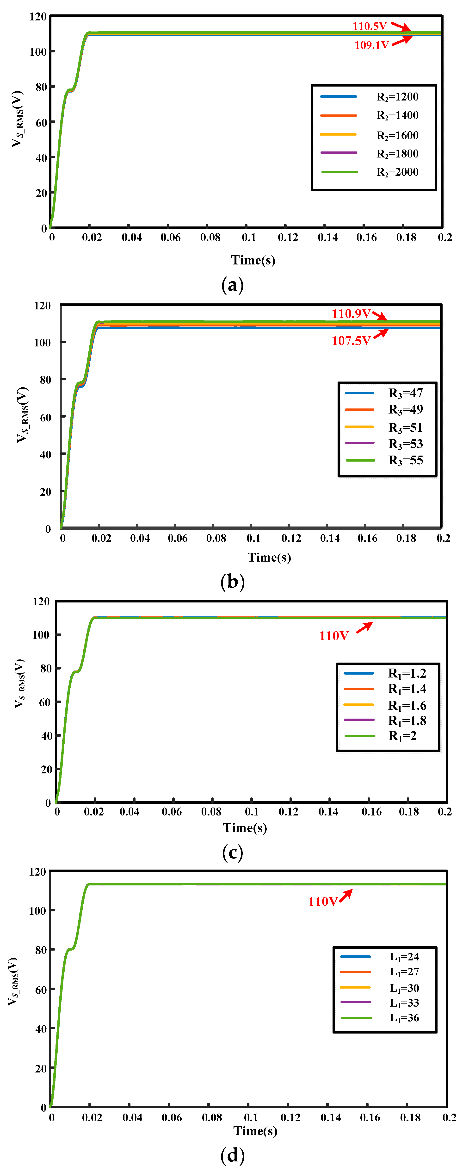
4.4. Sensitivity Analysis of Circuit Parameters
In order to verify the influences of the circuit parameters on the controller, sensitivity analysis is carried out based on Matlab/Simulink, as shown in Figure 9, where only one parameter is scanned in each subfigure.
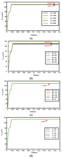
Figure 9.
The sensitivity analysis based on dead-beat with the observer and δ control. (a) CL varies; (b) non-critical load (NCL) varies; (c) Line resistance varies; (d) Line inductance varies.
Figure 9a–d show the results of sensitivity analysis on CL, NCL, line resistance, and line inductance, respectively. It is seen that the variations of the CL, line resistance, and line inductance have negligible effects on the controller. Although the NCL has more effects compared with others, it can be ignored since the values of NCLs are almost fixed in real applications. The results have verified that the proposed controller has good robustness, and also the CL voltage can be regulated well by the ES.
4.5. Discussions
It should be noticed that CL voltage is not the only control objective of the ES. It is easy to regulate the RMS value of CL voltage to follow the predefined value. However, the key point is the compensation mode of the ES which should be monitored. Another finding is that the proposed dead-beat controller with the help of an observer has the obvious advantage of eliminating harmonic components in CL voltage if compared to PR and P controllers. To increase the control precision and to make the δ control more practical, it is necessary to use the proposed control to replace the existing PR and P controls.
5. Conclusions
In this paper, dead-beat control cooperating with state observer for the state variables is proposed to work with existing δ control for the single-phase ESs. System modeling is executed and the discrete-time state space model is obtained. The operating principle and also the design process of the dead-beat control together with the observer is illustrated. Pure reactive power compensation and power factor correction, which present two typical operating modes of the ESs, are selected as examples to validate the proposed control and related analysis. By comparing the proposed control with existing controllers based on the same δ control algorithm, it is revealed that the proposed control has the obvious advantages of eliminating harmonic components in CL voltage during grid voltage distortion.
Author Contributions
Q.W. and W.Z. conceived the idea of this paper and performed the simulations and also wrote the paper, M.C., F.D. and G.B. provided guidance and revised the manuscript and added their thinking to validate the idea. All authors have equally contributed to the analysis and discussions.
Funding
This work was supported in part by the National Natural Science foundation of China (51877040 and 51320105002) and the Natural Science foundation of Jiangsu Province (BK20170675).
Conflicts of Interest
The authors declare no conflict of interest. The founding sponsors had no role in the design of the study; in the collection, analyses, or interpretation of data; in the writing of the manuscript, and in the decision to publish the results.
References
- Hui, S.Y.R.; Lee, C.K.; Wu, F. Electric springs—A new smart grid technology. IEEE Trans. Smart Grid 2012, 3, 1552–1561. [Google Scholar] [CrossRef]
- Wang, Q.; Cheng, M.; Chen, Z.; Wang, Z. Steady-state analysis of electric springs with a novel δ control. IEEE Trans. Power Electron. 2015, 30, 7159–7169. [Google Scholar] [CrossRef]
- Tan, S.C.; Lee, C.K.; Hui, S.Y.R. General steady-state analysis and control principle of electric springs with active and reactive power compensations. IEEE Trans. Power Electron. 2013, 28, 3958–3969. [Google Scholar] [CrossRef]
- Wang, W.; Yan, L.; Zeng, X.; Fan, B.; Guerrero, J.M. Principle and design of a single-phase inverter based grounding system for neutral-to-ground voltage compensation in distribution networks. IEEE Trans. Ind. Electron. 2017, 64, 1204–1213. [Google Scholar] [CrossRef]
- Hu, H.; Tao, H.; Blaabjerg, F.; Wang, X.; He, Z.; Gao, S. Train-network interactions and stability evaluation in high-speed railways—Part I: Phenomena and modeling. IEEE Trans. Power Electron. 2018, 33, 4627–4642. [Google Scholar] [CrossRef]
- Gong, Z.; Wu, X.; Dai, P.; Zhu, R. Modulated model predictive control for MMC-based active front-end rectifiers under unbalanced grid conditions. IEEE Trans. Ind. Electron. 2018. [Google Scholar] [CrossRef]
- Wang, Y.; Chen, Z.; Wang, X.; Tian, Y.; Tan, Y.; Yang, C. An estimator-based distributed voltage predictive control strategy for AC islanded microgrids. IEEE Trans. Power Electron. 2017, 30, 3934–3951. [Google Scholar] [CrossRef]
- Li, K.; Xu, H.; Ma, Q.; Zhao, J. Hierarchy control of power quality for wind-battery energy storage system. IET Power Electron. 2014, 7, 2123–2132. [Google Scholar] [CrossRef]
- Guerrero, J.M.; Vasquez, J.C.; Matas, J.; Matas, J.; de Vicuna, L.G.; Castilla, M. Hierarchical control of droop-controlled AC and DC microgrids—A general approach toward standardization. IEEE Trans. Ind. Electron. 2011, 58, 158–172. [Google Scholar] [CrossRef]
- Cheng, M.; Zhu, Y. The state of the art of wind energy conversion systems and technologies: A review. Energy Convers. Manag. 2014, 88, 332–347. [Google Scholar] [CrossRef]
- Chaudhuri, N.R.; Lee, C.K.; Chaudhuri, B.; Hui, S.Y.R. Dynamic modeling of electric springs. IEEE Trans. Smart Grid 2014, 5, 2450–2458. [Google Scholar] [CrossRef]
- Mok, K.T.; Tan, S.C.; Hui, S.Y.R. Decoupled power angle and voltage control of electric springs. IEEE Trans. Power Electron. 2016, 31, 1216–1229. [Google Scholar] [CrossRef]
- Wang, Q.; Cheng, M.; Jiang, Y.; Zuo, W.; Buja, G. A simple active and reactive power control for applications of single-phase electric springs. IEEE Trans. Ind. Electron. 2018, 65, 6291–6300. [Google Scholar] [CrossRef]
- Chen, X.; Hou, Y.; Tan, S.C.; Lee, C.K.; Hui, S.Y.R. Mitigating voltage and frequency fluctuation in microgrids using electric springs. IEEE Trans. Smart Grid 2015, 6, 508–515. [Google Scholar] [CrossRef]
- Yan, S.; Tan, S.C.; Lee, C.K.; Chaudhuri, B.; Hui, S.Y.R. Electric springs for reducing power imbalance in three-phase power systems. IEEE Trans. Power Electron. 2015, 30, 3601–3609. [Google Scholar] [CrossRef]
- Buso, S.; Caldognetto, T.; Brandao, D.I. Dead-beat current controller for voltage-source converters with improved large-signal response. IEEE Trans. Ind. Appl. 2016, 52, 1588–1596. [Google Scholar] [CrossRef]
- Young, H.A.; Perez, M.A.; Rodriguez, J.; Abu-Rub, H. Assessing finite-control-set model predictive control: A comparison with a linear current controller in two-level voltage source inverters. IEEE Ind. Electron. Mag. 2014, 8, 44–52. [Google Scholar] [CrossRef]
- Wassinger, N.; Penovi, E.; Retegui, R.G.; Maestri, S. Open-circuit fault identification method for interleaved converters based on time domain analysis of the state observer residual. IEEE Trans. Power Electron. 2018. [Google Scholar] [CrossRef]


© 2018 by the authors. Licensee MDPI, Basel, Switzerland. This article is an open access article distributed under the terms and conditions of the Creative Commons Attribution (CC BY) license (http://creativecommons.org/licenses/by/4.0/).