Abstract
Laser welding of copper is characterized by low and unstable light absorption around 1000 nm wavelength. Combination of high thermal conductivity and low melting point makes it difficult to obtain good welding quality and leads to low energy utilization. To improve efficiency and welding quality, a technique to enhance process stability using 1064 nm wavelength Nd:YAG laser has been proposed, and absorption rate and molten volume in laser micro-welding were discussed. Since the surface state of specimen affects absorption phenomena, effects of surface shape and surface roughness were investigated. Absorption rate and molten volume were increased by creating appropriate concave holes and by controlled surface roughness. Stable micro-welding process with deep penetration and good surface quality was achieved for transitional processing condition between heat conduction and keyhole welding, by enhanced absorption rate.
1. Introduction
The advances in laser technology have increased its competitiveness in various industrial fields, and this has enhanced its increased applications to various processes such as cutting [1], welding, and, more lately, for mechanical characterization [2]. In this work, laser was used for welding of copper. Copper finds great applications in automotive and renewable energy industries, since it is an important material for conducting electric power and for building up electrical systems. Miniaturization of products has necessitated micro-joining of copper in these fields. However, it is challenging to raise the temperature of copper locally owing to its high thermal conductivity and joining using conventional processes result in welding defects [3]. In addition, copper shows low light absorption rate around 1000 nm wavelength, which results in process instability [4]. The absorption rate of copper increases rapidly below 600 nm wavelength. Otte et al. reported the possibility of process stabilization at a wavelength of 532 nm [5]. Nakashiba et al. also developed a 532 nm wavelength green Nd:YAG laser and they investigated its performance in copper welding. They reported a stable process with high efficiency, which led to a narrow weld bead with deep penetration. Absorption rate of copper increased stably with increase in pulse duration, while pulse shaping helped to control porosity [6].
When near infrared light of 1064 nm fundamental wavelength Nd:YAG laser is used to micro-weld copper, the absorption rate increases with increasing power density. Green Nd:YAG laser of 532 nm wavelength shows higher and constant absorption rate regardless of change in power density. However, the power of the 532 nm laser system decreases because of frequency doubling of the Nd:YAG laser. Moreover, the 532 nm laser system is more complex and expensive compared to fundamental wavelength laser systems [7]. Therefore, shorter wavelength has a possibility of high efficient process for copper, but use of 1064 nm is desired in industrial applications because of its affordable cost and high reliability. However, since light absorption rate is very low at 1064 nm wavelength, stabilization of the process at this wavelength is challenging.
Creation of surface ripples during keyhole generation affects surface absorptivity [8]. Jae et al. investigated keyhole behavior in laser welding and they showed that light absorption is increased by multi-reflections effect in the keyhole [9]. Dowden et al. also investigated the process behavior in keyhole welding and they reported that most of the laser power was absorbed within the keyhole [10].
Bono et al. carried out laser welding of copper thin sheets using green and infrared pulsed laser beam sources and they noted that low absorptivity of copper increased sensitivity to variations in surface roughness and oxidation [11]. These characteristics lead to a highly sensitive and unstable process in laser welding of copper. Chen et al. investigated laser welding under four different surface conditions namely; as received, sandblasted, black-painted and nano-composite material added on pure copper surface. The highest welding efficiency was obtained by applying the nano-composite material on the surface of pure copper coupons. The sandblast surface treatment and black-painting could also decrease the surface reflectivity from the laser beam and thus enhanced welding efficiency [12]. Engler et al. have also noted that with low laser absorption, changing surface conditions leads to a highly sensitive process. In addition, infrared light absorption increases remarkably at the transition region between solid phase and liquid phase [13].
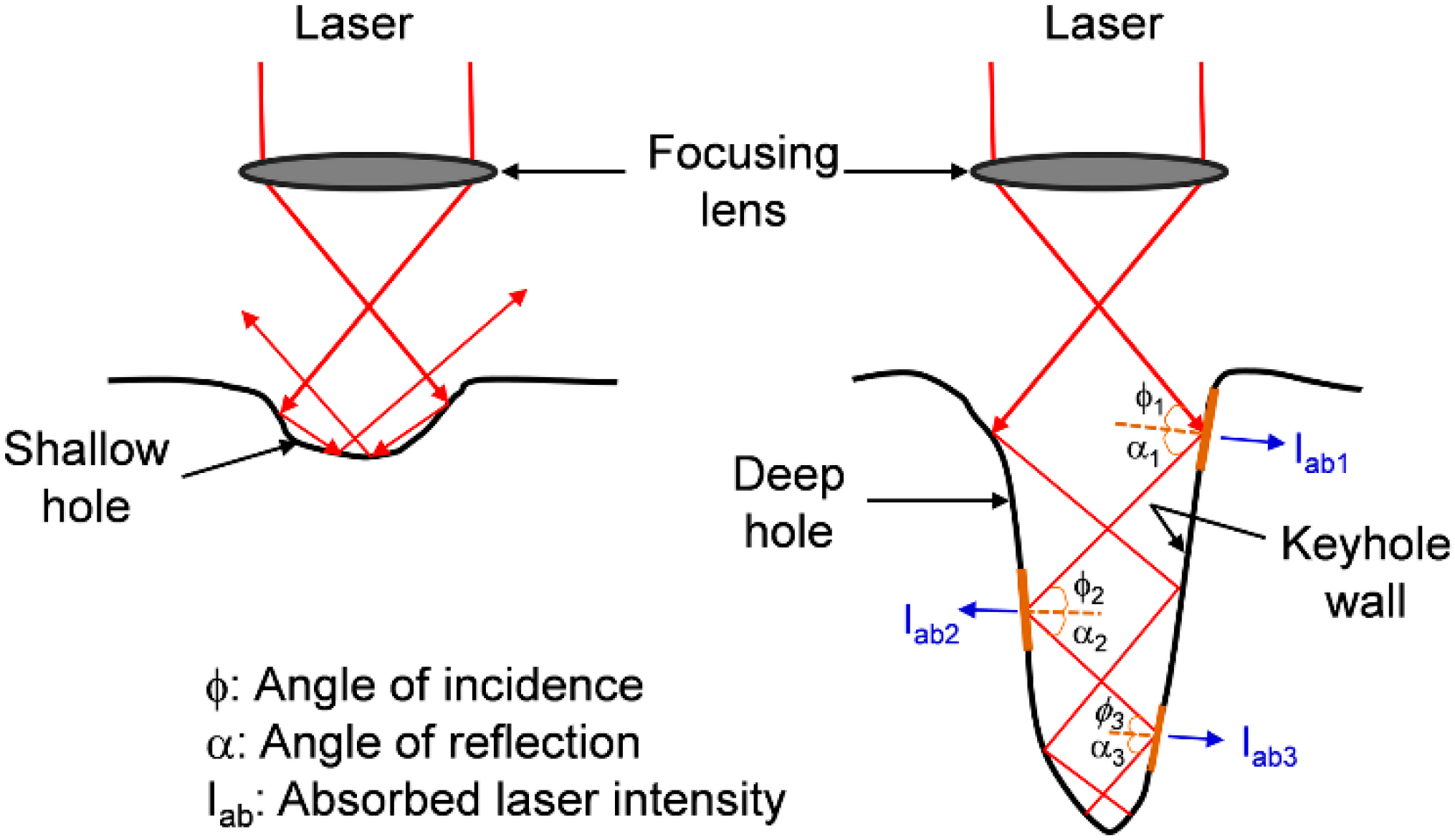
Since the absorption rate by fundamental wavelength of Nd:YAG laser increases because of multi-reflections effect on the keyhole wall, it is expected that the absorption rate might increase by irradiating the laser on the wall of a concave hole similar to a keyhole. Moreover, surface roughness of workpiece would affect absorption phenomenon of laser beam. There is a minimum depth required to ensure multi-reflections effect within the keyhole. A shallow keyhole means that the reflection will be directed to the surrounding as shown in Figure 1. By considering Fresnel absorption, part of the incident laser energy is reflected by keyhole walls, while part is absorbed within the keyhole walls. The angle of incidence of laser beam is equal to the angle of reflection at the interface of liquid and vapor. In actual phenomenon, some of the energy will be lost within the keyhole by plasma absorption [14,15].
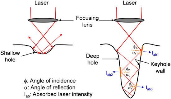
Figure 1.
Schematic illustration of multi-reflections effect inside the keyhole.
Bergstrom et al. employed ray tracing technique to study Nd:YAG laser absorption behavior on both smooth and rough surfaces. They showed that for light which is normally incident to the surface, the absorption rate increases with increase in roughness, but for tangentially incident light, the relationship between absorption rate and surface roughness is intricate [16]. However, these effects on welding characteristics of copper have not been fully clarified yet. Therefore, effects of surface shape and surface roughness on absorption characteristics were experimentally investigated using 1064 nm Nd:YAG laser in order to improve the absorption rate for stable welding of copper.
2. Materials and Methods
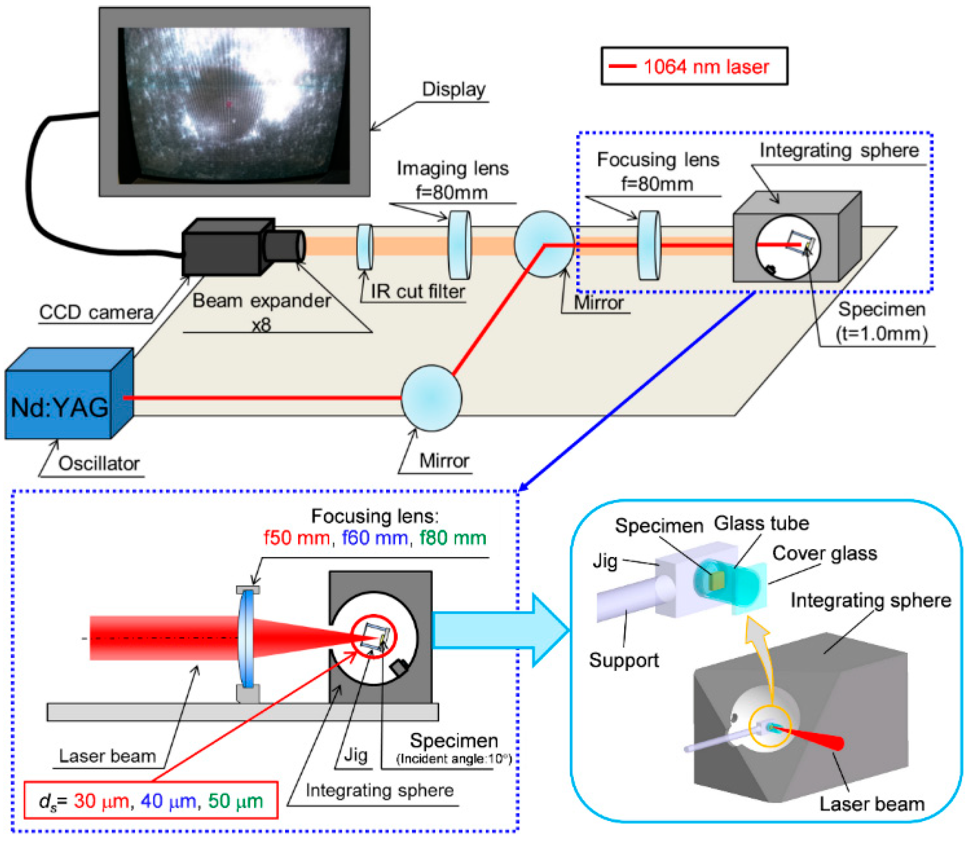
Micro-welding of oxygen-free copper, C1020 was performed by using 1064 nm wavelength Nd:YAG laser (KLY-HP300α, Kataoka Corporation, Kyoto, Japan). The physical properties of copper C1020 are summarized in Table 1 [6,17,18]. The experimental setup for the measurement of absorption rate is shown in Figure 2. The copper specimen was mounted in an integrating sphere (F100A-IS, Ophir Japan Ltd, Saitama, Japan), which was filled with nitrogen gas to prevent oxidation of the workpiece. The absorption rate was evaluated by measurement of reflected energy inside the integrating sphere. The inner surface of the integrating sphere was coated with barium sulfate, which is a highly reflective material. The specimen was set at the center of the integrating sphere. The detector was located along the inner surface of the integrating sphere, and there were no time dependent variations during the measurement process.

Table 1.
Physical properties of copper C1020.

Figure 2.
Schematic illustration of experimental setup for measurement of absorption rate.
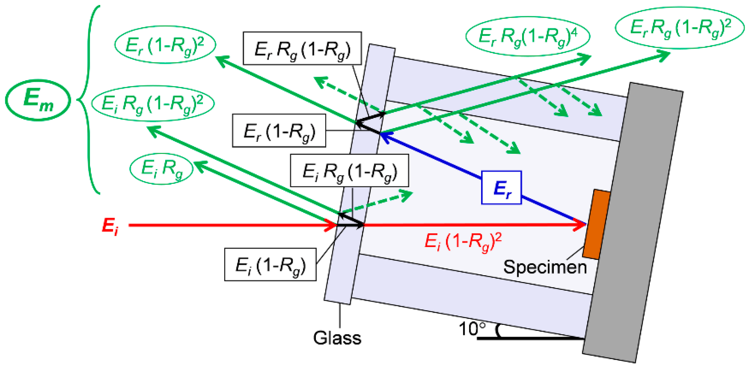
To prevent scattering of spatter, the specimen was set in a quartz glass tube with inner diameter of 6.0 mm and outer diameter of 8.0 mm. The opening of the tube was sealed with a 0.3 mm thick cover made of borosilicate glass. The specimen size was 4.0 mm in length, 4.0 mm in width, and 1.0 mm in thickness. To prevent the cover glass from being damaged by plasma pressure or metal vapor generated during processing, a pressure releasing hole was provided in the jig used to fix the specimen. The reflection loss caused by the glass plates was considered when calculating the absorption rate, as shown in Figure 3.
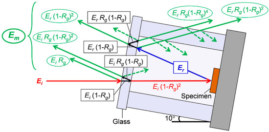
Figure 3.
Illustration of reflection loss by glass plates inside the integrating sphere.
The initial energy from the irradiated laser beam is Ei, the energy measured by the sensor in the integrating sphere is Em, and the energy reflected by the specimen is Er. The reflectance of the copper specimen and the glass are Rw and Rg, respectively. In this case, the incidence angle was assumed to be at the lower level below 45 degrees, and the reflectivity from air to glass and vice versa was assumed to be of the same value. The incident laser beam is reflected twice by the cover glass before reaching the specimen surface. Thus, the relationship between the incident light energy Ei and the transmitted light energy Ei2 is given by Equation (1).
The incident energy Ei was measured by irradiating the laser beam inside the integrating sphere with no specimen in place. In addition, the value of transmittance for the cover glass used in this experiment was measured to be 91.8%. Using Equation (1), the reflectance of glass Rg was calculated to be approximately 4%. The energy reflected by the specimen inside the integrating sphere Er is as expressed by Equation (2).
Considering the reflection loss due to the glass plates, the total reflected energy was computed as shown by Equation (3), while the absorption rate was computed according to Equation (4). Second reflection by the back side of the glass was ignored in the computation since its value was very small, hence negligible. This second reflection is shown by the dashed arrows in Figure 3.
where α is the absorption rate (%) and Ea is the absorbed energy (J).
To study the effect of surface shape on absorption rate, concave holes were created on the workpiece surface using a compression testing machine (EZ-L, Shimadzu Corporation, Kyoto, Japan) with a cone tool made of polycrystalline diamond (PCD), in which the angle of tool tip was 45 degrees. Eight different depths were made by applying different loads as shown in Table 2.

Table 2.
Variation of concave dimensions with applied load.
To investigate the effects of surface roughness, various roughened surfaces were obtained by using silicon carbide abrasive papers with different grain sizes. Surface roughness was measured using a stylus type roughness measurement machine (SURFCOM 1400D, Tokyo Seimitsu Co., Ltd, Tokyo, Japan) which had a stylus radius of 2 μm.
For the laser micro-welding experiment, the laser beam was focused onto the workpiece surface such that spot diameters of 30 μm, 40 μm, and 50 μm were obtained by using focusing lenses with focal lengths of 50 mm, 60 mm, and 80 mm, respectively. Then, input diameter into the focusing lens was appropriately controlled to obtain the required spot diameter. A single shot of laser pulse with a rectangular waveform and a pulse duration of 1.2 ms was used. The workpiece was inclined by approximately 10 degrees against the laser beam axis during the process. A CCD camera (Sony XC-75, Sony Corporation, Tokyo, Japan) was used to ensure that the laser was irradiated accurately inside the concave holes. Laser irradiation was done at the bottom center of the concaves as well as the inner walls of the concave holes. In order to suppress oxidation during the process, nitrogen gas was supplied to the irradiation area at a flow rate of 50 L/min, using a nozzle of 9.0 mm inner diameter. Besides evaluation of absorption rate, the molten volume was also calculated using measurements of the observed cross-section. The total molten part was divided into three different parts, namely; semi-ellipsoid, cylinder, and cylindrical segment. Using mathematical equations, the different volumes were computed. The volume of concave hole that was created using the PCD tool was subtracted from the total sum of the volumes to give the amount of molten volume. To evaluate the cross-section, the specimen was polished and then treated with nitric acid of 65.0% weight concentration. Additional treatment was done with a mixed solution of ammonia and hydrogen peroxide with 15.6% weight concentration. An optical microscope (VHX-2000, Keyence Corporation, Osaka, Japan) and a scanning electron microscope (SEM) (JSM-7001F, JEOL Ltd, Tokyo, Japan) were used to capture images of the cross-sections and irradiated surfaces, respectively.
3. Results and Discussion
3.1. Influence of Surface Shape on Absorption Rate
High power density is required for deep penetration. Under no-melting condition, the power density is not enough to cause melting of the material. In this study, this condition was experienced when the power density was below 1.0 × 10⁸ W/cm2. Higher power density sufficient to melt the material but insufficient to cause boiling leads to heat conduction welding mode. Heat is transferred into the material by heat conduction. Convection phenomenon also plays a role once a weld pool is formed. This conduction mode welding does not penetrate into the material. The process takes place in both vertical and horizontal directions along the surface of the material, hence the semi-circular shape of the weld bead cross-section. This condition was achieved in the power density region between 1.0 × 10⁸ W/cm2 and 1.7 × 10⁸ W/cm2. The heat conduction welding mode is stable since there is no vaporization, and there is no further absorption below the surface of the material. With considerably high power density, boiling of the material is achieved, hence the creation of a keyhole in the melt pool. This leads to keyhole welding mode. The keyhole is filled with plasma and can extend over the full thickness of the material. The plasma flows out of the keyhole and forms plasma plume above the material. To protect the weld from oxidation, a shielding gas is employed. In this study, nitrogen was used as the shielding gas. The keyhole can be unstable owing to its intermittent oscillations and closing. This instability causes porosity due to the gas being held within the keyhole, and this may lead to embrittlement of joint [19,20]. Keyhole welding mode was achieved with power densities above W/cm2.
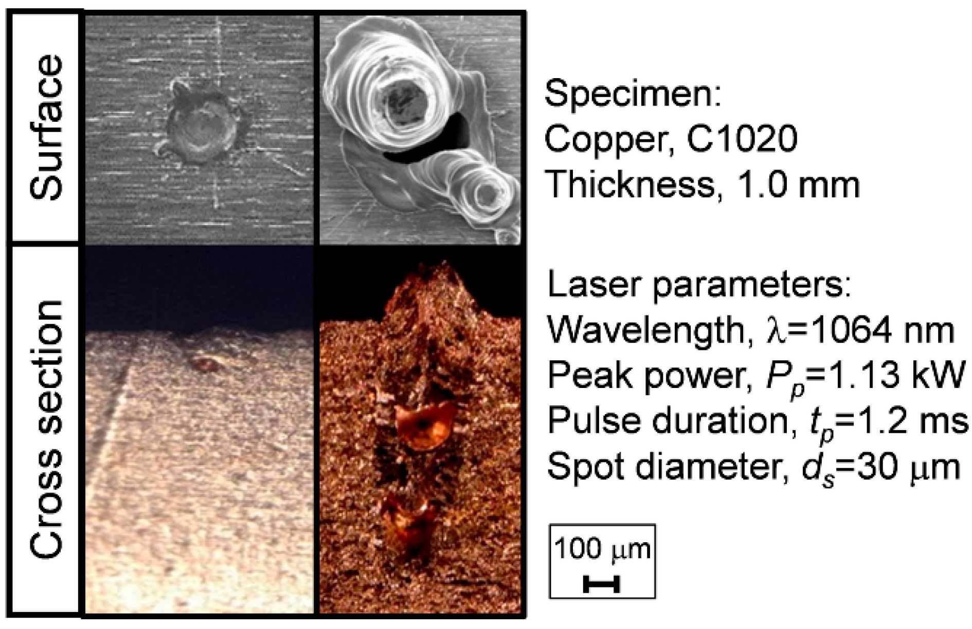
In this study, transitional processing condition refers to the region between the two modes of heat conduction and keyhole welding. In this region, the processing consists of a mixture of the two modes. This transition region was in the power density range between W/cm2 and W/cm2. Under this transitional processing condition, it is possible to stabilize the process, and thus generate large penetration depth with no porosity, and to achieve good surface quality. By using peak power around 1.13 kW, transitional processing condition between heat conduction and keyhole welding modes was achieved using a rectangular waveform with a pulse duration of 1.2 ms. Figure 4 shows photographs for the irradiated flat surface and cross-section under transitional processing condition.
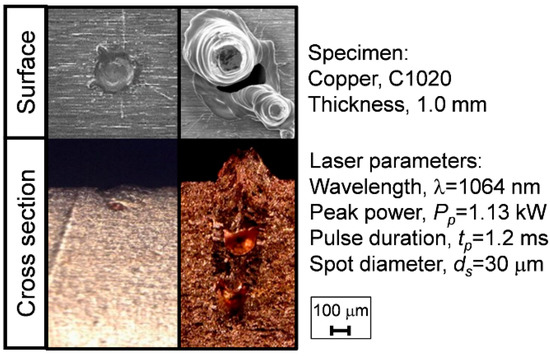
Figure 4.
Molten area appearance under transitional processing condition between heat conduction and keyhole welding modes.
Nakashiba et al. have reported the possibility of obtaining good surface quality through process stabilization at the transition region between heat conduction and keyhole welding [21]. Auwal et al. have noted that low process stability has disadvantages of porosity and spatter generation [22]. Improvement of welding stability makes 1064 nm wavelength laser useful in copper welding. Therefore, in this study, a stable keyhole was generated under transitional processing condition by utilizing the effect of increasing light absorption rate with surface undulation.
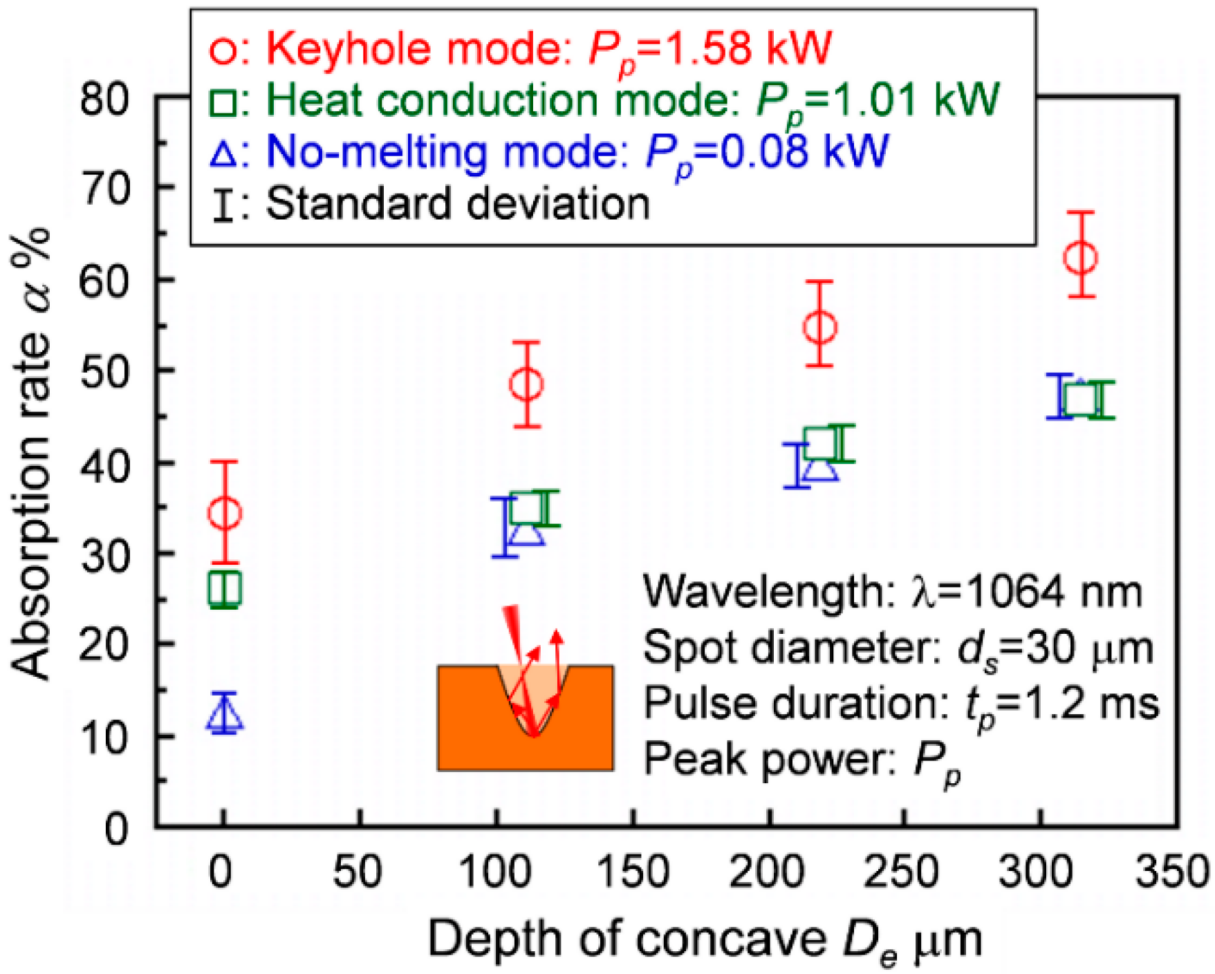
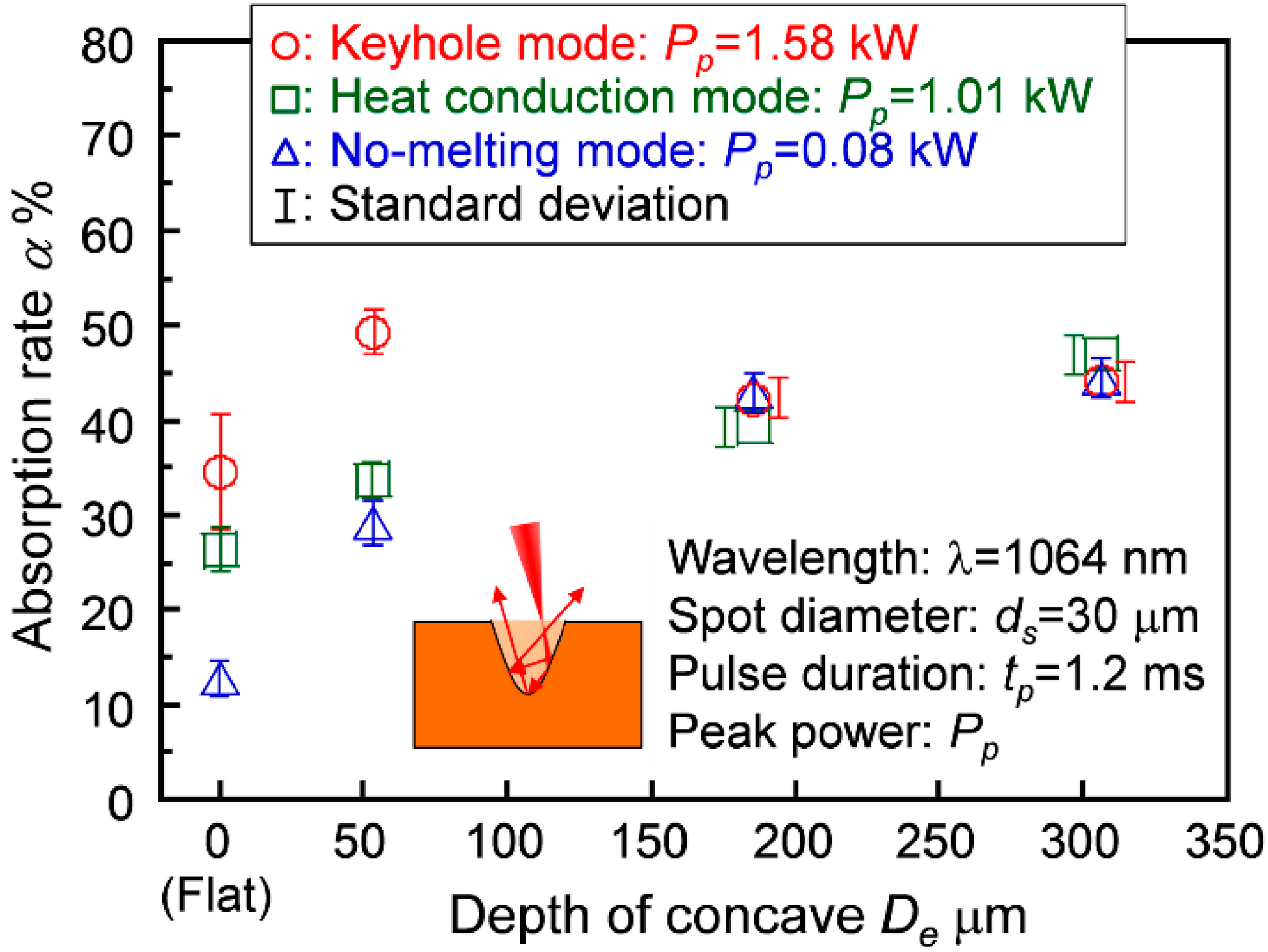
Figure 5 shows the light absorption rate of 1064 nm wavelength laser on a flat surface and under concave holes of different depths. Irradiation was done at the bottom center of the concave holes. Figure 6 shows processing results under same conditions as Figure 5, but with irradiation on the walls of the concave holes.
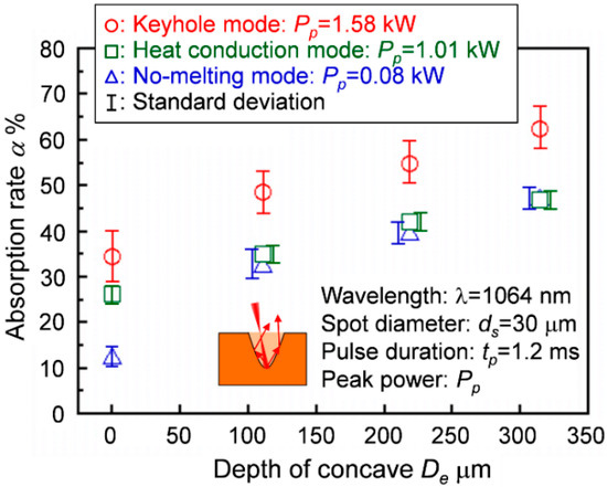
Figure 5.
Variations of absorption rate with concave depths for irradiation at bottom center of concave.
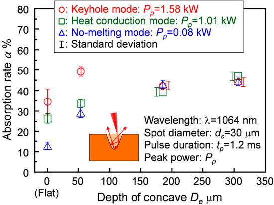
Figure 6.
Variations of absorption rate with concave depths for irradiation on concave walls.
In comparison to the flat surface, the light absorption rate under concave holes increases in all the welding modes for both irradiation positions. However, for irradiation on the concave walls under keyhole welding mode, the absorption rate was not affected by increased depth of concave and thus showed a constant value. Therefore, to clearly show the influence on surface shape, irradiation should be done at the bottom center of the concave holes.
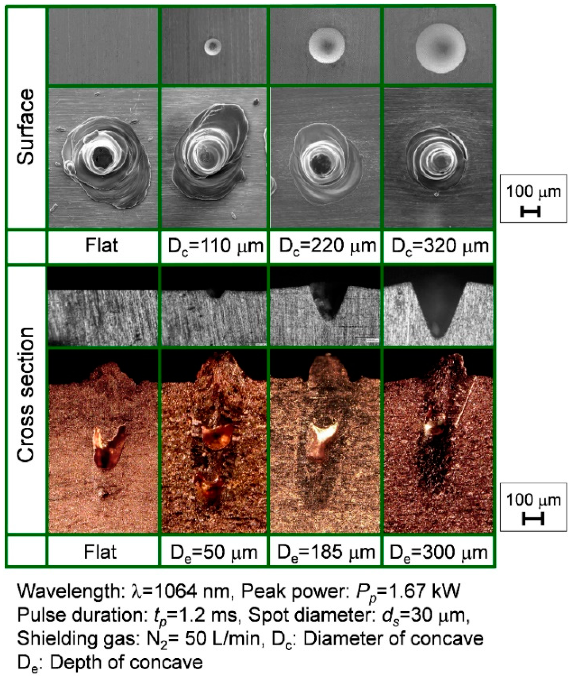
Figure 7 shows the observed surfaces and cross-sections under keyhole welding mode for flat surface and when various concave depths were prepared, with irradiation at the bottom center of the concave holes. Also shown are the appearances of the surfaces and cross-sections before laser irradiation.

Figure 7.
Surface and cross-section appearances for flat surface and various concave holes before and after keyhole welding, with irradiation at bottom center of concave.
Using high peak power of 1.67 kW, stable keyhole welding condition could be achieved irrespective of changes in light absorption rate under conditions of flat surface and different concave depths, but there was the disadvantage of porosity. Lowering the power to 1.13 kW led to a condition of transitional processing between heat conduction and keyhole welding modes. As shown in Figure 4, this transitional condition is unstable, but it was stabilized leading to deep penetration with no porosity generation.
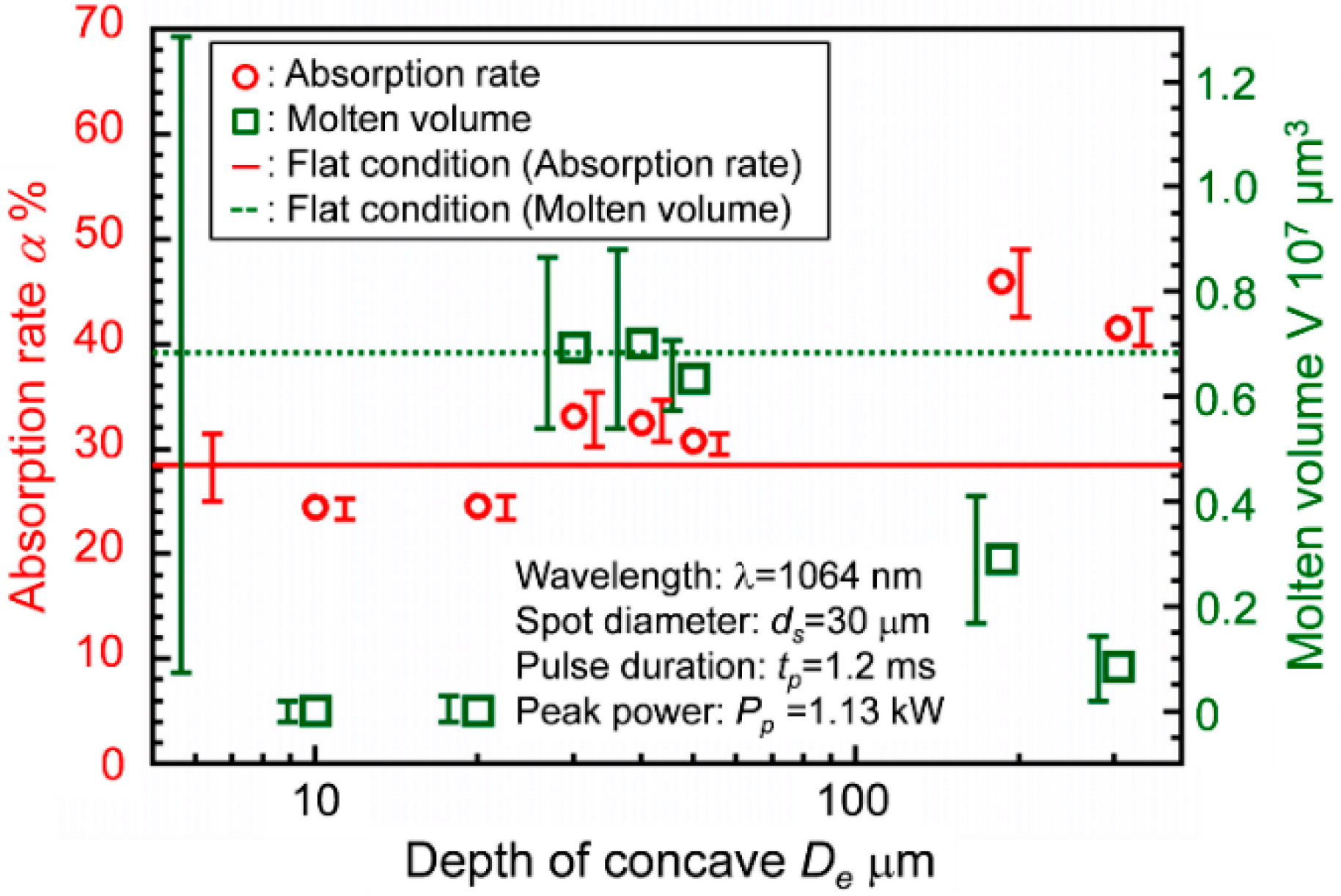
Figure 8 shows variations of light absorption and molten volume for different concave depth under transitional processing condition. The horizontal lines indicate changes in the absorption rate and molten volume for a flat surface. When irradiating the laser beam on a flat surface, heat conduction and keyhole welding modes are combined, and the standard deviations of light absorption rate and molten volume are large. For depths of concave at 10 μm and 20 μm, only heat conduction welding mode exists and the molten volume is small compared to that under flat surface. On the contrary, the light absorption increases in the concave depths between 30 μm to 50 μm, and its standard deviation becomes small. The molten volume also increases corresponding to the change of absorption rate, and stable keyhole welding mode can be obtained. Molten volume decreases in the concave shape condition with depth of more than 100 μm. This is because as the laser is focused on the specimen surface, the position of the convergence point is deviated by the depth of the concave hole, and the power density is lowered. Therefore, under transitional processing condition, concave holes of a certain appropriate depth help to stabilize the absorbed energy, hence stabilizing the process.
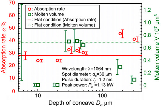
Figure 8.
Variations of light absorption and molten volume for different concave depths under transitional processing condition between heat conduction and keyhole welding modes.
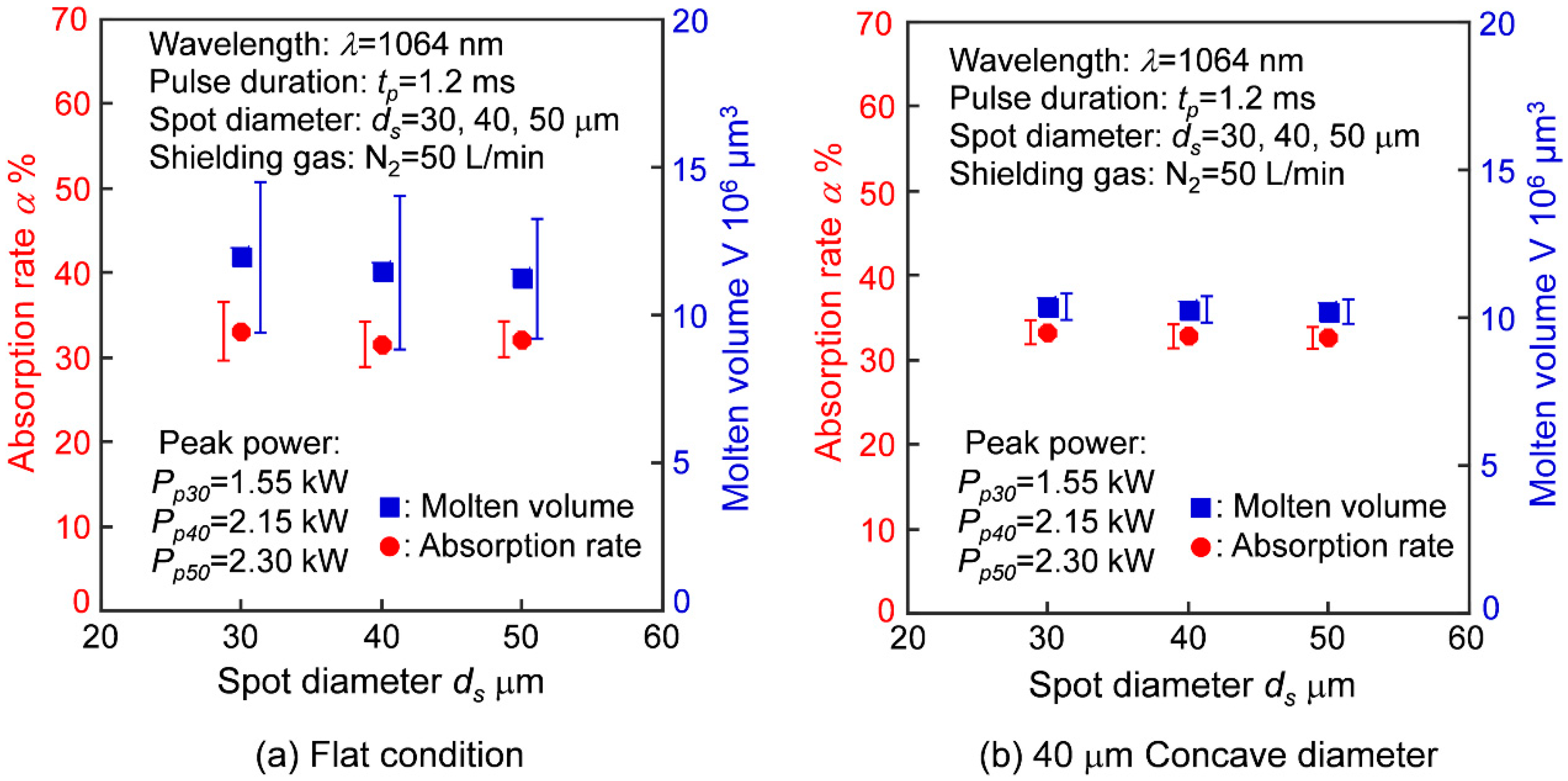
Figure 9 shows the variations of absorption rates and molten volumes with spot diameters of 30 μm, 40 μm, and 50 μm, under conditions of flat surface and with concave diameter of 40 μm. The power density was maintained at a constant by using different peak powers for each case. This part of the study aimed at showing how positional accuracy of the laser irradiation on the work-piece surface influences the absorption rate and molten volume. Under flat surface condition, the standard deviations were large and the process was unstable. On the other hand, with 40 μm concave diameter, the absorption rate was stabilized, leading to a stable molten volume. Thus, it is evident that, by maintaining the power density and providing a suitable concave hole, the micro-welding process can be stabilized. It was possible to obtain almost equivalent light absorption rate and molten volume regardless of the change in spot diameter, by maintaining the spot size at about ±25% of the concave hole diameter. Therefore, when a concave hole is provided, there should be concern about the positional relationship between the laser beam and the concave hole, but a limited certain positional deviation can be tolerated. In addition, an appropriate diameter of the concave hole is required since it will determine the irradiation point of the laser beam. A smaller diameter means that the laser beam is not fully irradiated inside the concave. Moreover, the concave diameter determines the slope of the concave walls, which bears a great influence on the multi-reflections effect shown in Figure 1. It is noted that increase in laser spot size under constant laser power leads to reduction in power density, hence reduction in effective laser energy on the micro-welding process. Thus, further investigation on the influence of spot size should be done.
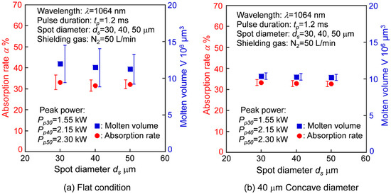
Figure 9.
Variations of absorption rate and molten volume with laser spot diameters.
3.2. Influence of Surface Roughness on Absorption Rate
High surface roughness means that reflection of light to the surrounding is reduced and keyhole multi-reflections effect is increased, as illustrated in Figure 1. This results in an increase of the absorption rate. Consequently, high absorption rate results in higher molten volume, hence leading to an effective welding process. Thus, proper control of surface roughness can contribute to improvement of 1064 nm laser absorption rate and its stability. Figure 10 shows typical appearances of copper surfaces and cross-sections for different roughness values, before and after laser irradiation.
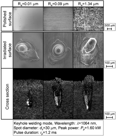
Figure 10.
Observed surfaces and cross-sections for different surface roughness values.
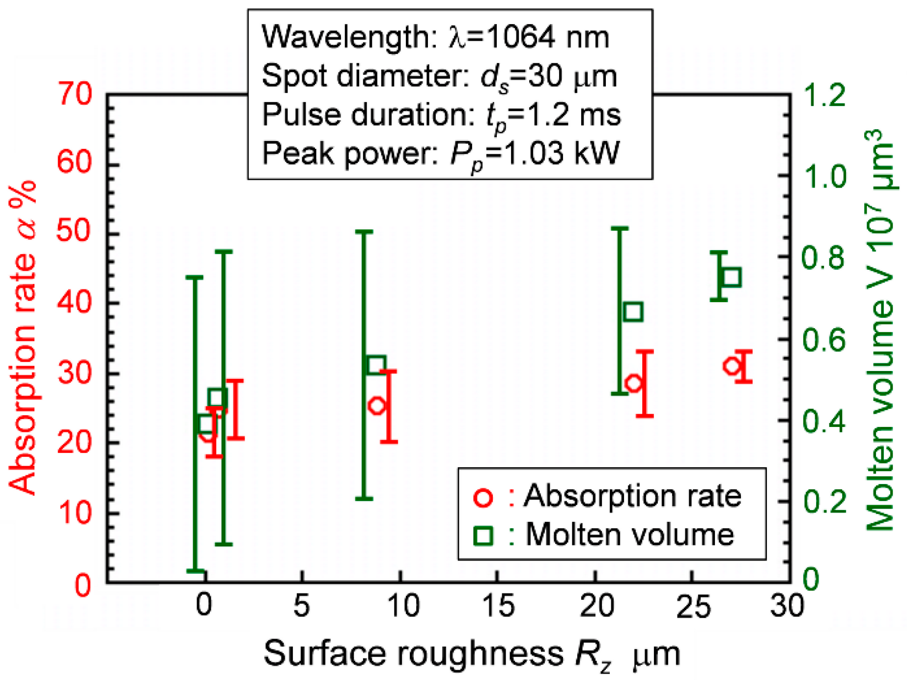
Figure 11 shows the variations of absorption rate and molten volume with surface roughness Rz under transitional processing condition between heat conduction and keyhole welding modes for 1064 nm wavelength Nd:YAG laser. When surface roughness Rz is small, unstable welding prevails where heat conduction and keyhole welding modes are combined. The values of both light absorption rate and molten volume are small. However, as surface roughness Rz increases, the occurrence rate of keyhole welding mode prevails against heat conduction welding mode, and light absorption rate and molten volume increase. When surface roughness Rz is about 27 μm, the light absorption rate and molten volume are the largest, and stable welding can be obtained. Considerably higher values of surface roughness above 30 μm result in unstable keyhole welding phenomenon, with reduced molten volume. It is expected that with roughness Rz above 30 μm, the depth of surface undulations is considerably increased and this might lead to deviation of laser convergence point, hence reduction in absorption rate leading to an inefficient process. Therefore, stable welding can be achieved when surface roughness Rz is around 30 μm, a depth similar to concave, as indicated in Figure 8.
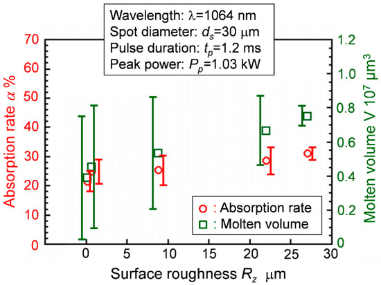
Figure 11.
Variations of absorption rate and molten volume with roughness under transitional processing condition between heat conduction and keyhole welding modes.
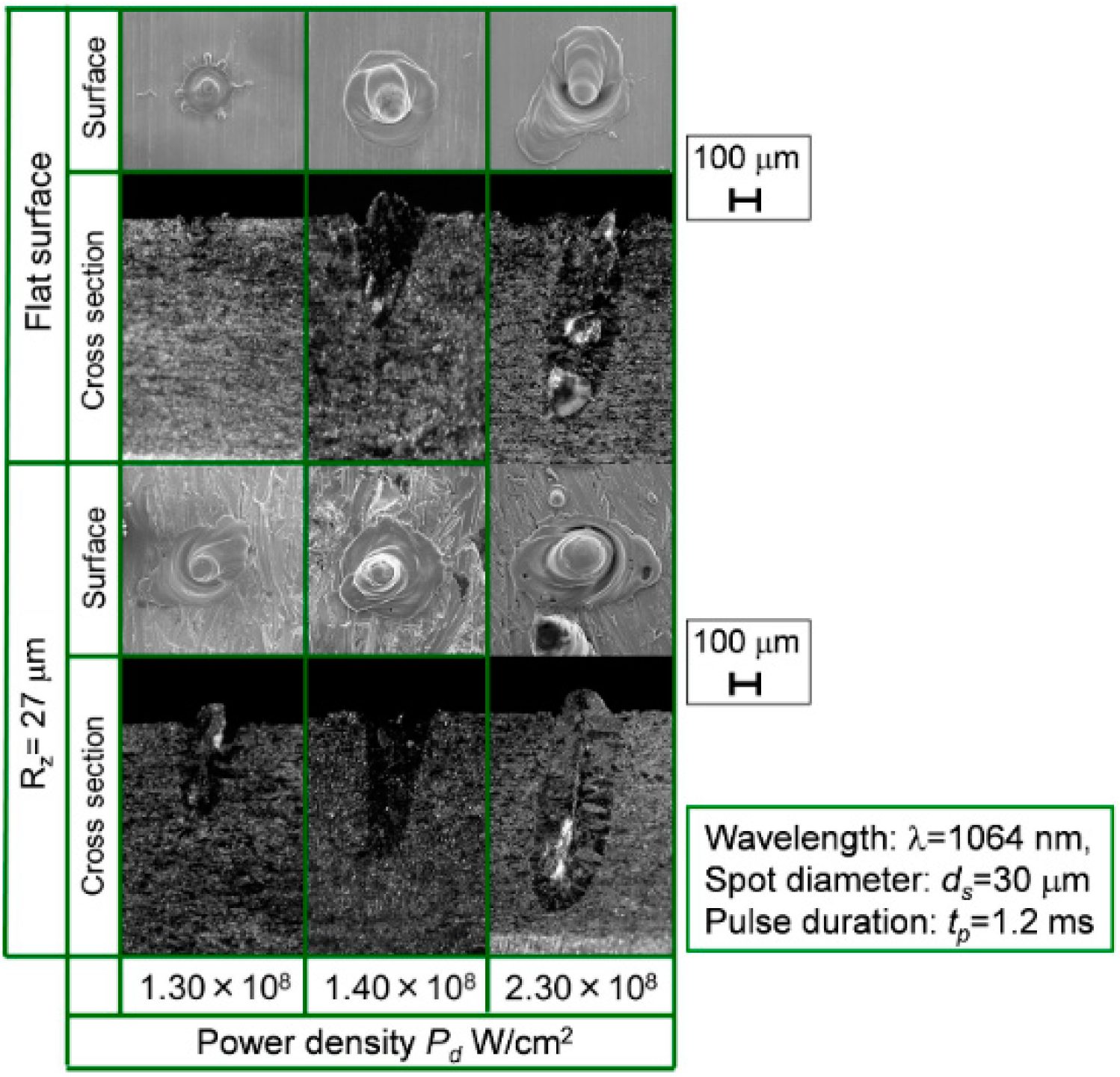
Figure 12 shows the observed surfaces and cross-sections, when different power densities were used, with specimen surfaces set to flat condition and roughness Rz of 27 μm.
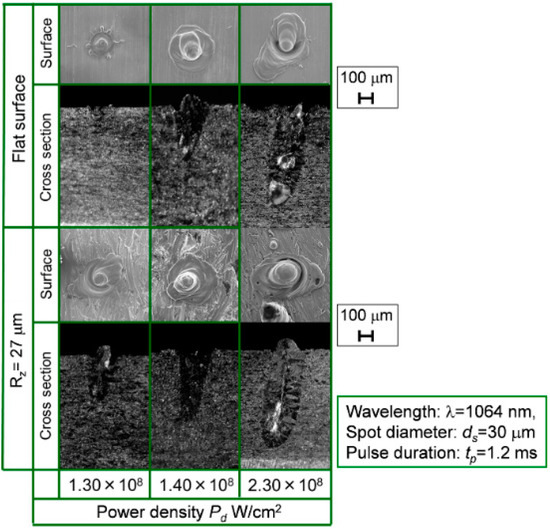
Figure 12.
Observed surfaces and cross-sections for different power densities in the case of flat surface and Rz = 27 μm.
In deep penetration condition with power density up to 2.3 × 10⁸ W/cm2, porosity and spattering occur, leading to a bad weld. On the contrary, transitional processing condition between heat conduction welding and keyhole welding modes, with power density of around 1.4 × 10⁸ W/cm2, generates a stable keyhole and surface texture can be controlled. Under this condition, porosity and spattering are reduced compared to deep penetration condition. This is an ideal condition to obtain sufficient penetration and good surface quality. Therefore, with low power density, it is possible to reduce weld defects by controlling the surface topology, and thus obtain a stable welding process.
The tilt of the specimen surface and slope variations on the specimen surface affect the effective cone angle of light from a lens. This cone angle is directly related to the effective numerical aperture (N.A.), which determines the size of the focus spot [23,24,25]. The focus spot diameter is directly proportional to the wavelength of the laser and inversely proportional to the N.A. of the focusing lens [19,20]. Consequently, the relationship between surface profile variations and N.A. is of great influence to the process. Thus, the relationship of surface roughness and N.A., and the resulting influence on laser absorption rate should be investigated.
It is considered that surface topology has a great influence on absorption rate for 1064 nm laser. The control of surface texture is effective to improve the stability of welding phenomena when using 1064 nm laser, and approximately 30 μm surface variation would be proper to achieve a large molten volume with a small deviation.
4. Conclusions
High efficiency and high quality laser welding of copper is expected by using an appropriate approach. Stable micro-welding with 1064 nm Nd:YAG laser can be enhanced by utilizing the effect of increasing light absorption rate with controlled variations of surface topology. The following are the main conclusions deduced:
- Absorption rate and molten volume under 1064 nm wavelength laser is increased by controlled surface undulations such as creating appropriate concave holes, and by controlled surface roughness variations. There is correlation between the surface roughness and concave holes. Concave depth of around 30 μm and a similar value of surface roughness Rz leads to stabilization of the micro-welding process.
- For copper welding using 1064 nm laser, by optimizing the surface texture in transitional processing condition between heat conduction and keyhole welding, light absorption was improved and the process was stabilized leading to deep penetration and good surface quality.
Author Contributions
Conceptualization, M.R.M., Y.O., and R.I.; Methodology, M.R.M., Y.O., and R.I; Formal analysis, M.R.M., Y.O., and R.I.; Investigation, M.R.M. and R.I.; Resources, Y.O., A.O., S.-i.N., and T.S.; Writing—original draft preparation, M.R.M.; Writing—review and editing, M.R.M., Y.O., and A.O.; Supervision, Y.O. and A.O.; Funding acquisition, Y.O. and A.O.; Visualization, M.R.M. and Y.O.
Funding
This research was funded by JSPS KAKEN Grant Number 15K05725.
Acknowledgments
The authors acknowledge the support given by Japanese Ministry of Education, Culture, Sports, Science and Technology, and Jomo Kenyatta University of Agriculture and Technology, Kenya.
Conflicts of Interest
The authors declare no conflict of interest. The funders had no role in the design of the study; in the collection, analyses, or interpretation of data; in the writing of the manuscript, or in the decision to publish the results.
References
- Chryssolouris, G. Laser Machining-Theory and Practice (Mechanical Engineering Series), 1st ed.; Springer-Verlag: New York, NY, USA, 1991; ISBN 0-387-97498-9. [Google Scholar]
- Athanasiou, C.E.; Hongler, M.-O.; Bellouard, Y. Unraveling Brittle-Fracture Statistics from Intermittent Patterns Formed During Femtosecond Laser Exposure. Phys. Rev. Appl. 2017, 8, 054013. [Google Scholar] [CrossRef]
- Mai, T.A.; Spowage, A.C. Characterisation of dissimilar joints in laser welding of steel-kovar, copper-steel and copper-aluminium. Mater. Sci. Eng. A 2004, 374, 224–233. [Google Scholar] [CrossRef]
- Hess, A.; Schuster, R.; Heider, A.; Weber, R.; Graf, T. Continuous wave laser welding of copper with combined beams at wavelengths of 1030 nm and of 515 nm. Phys. Procedia 2011, 12, 88–94. [Google Scholar] [CrossRef]
- Otte, F.; Pamin, S.; Hermsdorf, J.; Kracht, D.; Kling, R. Enhancement of process stability for laser spot micro-welding by using 532 nm radiation. In Proceedings of the International Congress on Laser Advanced Materials Processing (LAMP), Kobe, Japan, 29 June–2 July 2009; pp. 09–114. [Google Scholar]
- Nakashiba, S.; Okamoto, Y.; Sakagawa, T.; Takai, S.; Okada, A. Micro-Welding of Copper Plate by Frequency Doubled Diode Pumped Pulsed Nd:YAG Laser. Phys. Procedia 2012, 39, 577–584. [Google Scholar] [CrossRef]
- Okamoto, Y.; Nakashiba, S.; Wada, T.; Sakagawa, T.; Nishi, N.; Okada, A. Characterization of Absorptivity in Micro-welding of Copper by Pulsed Green Nd:YAG Laser. In Proceedings of the International Congress on Applications of Lasers & Electro-Optics ICALEO, San Diego, CA, USA, 19–23 October 2014. [Google Scholar] [CrossRef]
- Fabbro, R.; Coste, F.; Slimani, S.; Briand, F. Study of keyhole behaviour for full penetration Nd:YAG CW laser welding. J. Phys. D Appl. Phys. 2005, 38, 1881–1887. [Google Scholar] [CrossRef]
- Jae, Y.L.; Sung, H.K.; Dave, F.F.; Choong, D.Y. Mechanism of keyhole formation and stability in stationary laser welding. J. Phys. D Appl. Phys. 2002, 35, 1570–1576. [Google Scholar] [CrossRef]
- Dowden, J.; Kapadia, P.; Postacioglu, N. An analysis of the laser-plasma interaction in laser keyhole welding. J. Phys. D Appl. Phys. 1989, 22, 741–749. [Google Scholar] [CrossRef]
- Bono, P.D.; Metsios, I.; Blackburn, J.; Hilton, P. Laser processing of copper and aluminum thin sheets with green (532 nm) and infrared (1064 nm) pulsed laser beam sources. In Proceedings of the 32nd International Congress on Applications of Lasers and Electro-Optics (ICALEO 2013), Miami, FL, USA, 6–10 October 2013; Volume 616, pp. 520–528. [Google Scholar] [CrossRef]
- Chen, H.-C.; Bi, G.; Nai, M.L.S.; Wei, J. Influence of surface condition in fiber laser welding of pure copper. In Proceedings of the 31st International Congress on Applications of Lasers and Electro-Optics (ICALEO 2012), Anaheim, CA, USA, 23–27 September 2012; Volume 615, pp. 558–564. [Google Scholar] [CrossRef]
- Engler, S.; Ramsayer, R.; Poprawe, R. Process Studies on Laser Welding of Copper with Brilliant Green and Infrared Lasers. Phys. Procedia 2011, 12, 339–346. [Google Scholar] [CrossRef]
- Al-Kazzaz, H.; Medraj, M.; Cao, X.; Jahazi, M. Nd:YAG laser welding of aerospace grade ZE41A magnesium alloy: Modeling and experimental investigations. J. Mater. Chem. Phys. 2008, 109, 61–76. [Google Scholar] [CrossRef]
- Jung-Ho, C.; Suck-Joo, N. Implementation of real-time multiple reflection and Fresnel absorption of laser beam in keyhole. J. Phys. D Appl. Phys. 2006, 39, 5372–5378. [Google Scholar] [CrossRef]
- Bergstrom, D.; Powell, J.; Kaplan, A.F.H. A ray-tracing analysis of the absorption of light by smooth and rough metal surfaces. J. Appl. Phys. 2007, 101, 113504. [Google Scholar] [CrossRef]
- Millard Wire & Specialty Strip Company. Available online: https://www.millardwire.com/ (accessed on 2 August 2018).
- Japan Society of Thermophysical Properties (JSTP). Thermophysical Properties Handbook; Yokendo Co. Ltd.: Tokyo, Japan, 2008. [Google Scholar]
- John, C.I. Laser Processing of Engineering Materials–Principles, Procedure and Industrial Application; Elsevier Butterworth-Heinemann: London, UK, 2005; pp. 41–70, 395–401. ISBN 0-7506-6079-1. [Google Scholar]
- Steen, W.M. Laser Material Processing, 3rd ed.; Springer-Verlag: London, UK, 2003; pp. 83–105, 157–165. ISBN 1-85233-698-6. [Google Scholar]
- Nakashiba, S.; Okamoto, Y.; Sakagawa, T.; Harada, M.; Okada, A. The boundary of keyhole generation in micro-welding of aluminum alloy by pulsed Nd:YAG laser with superposition of continuous diode laser. J. Jpn. Soc. For. Precis. Eng. 2014, 80, 419–424. [Google Scholar] [CrossRef]
- Auwal, S.T.; Ramesh, S.; Yusof, F.; Manladan, S.M. A review on laser beam welding of copper alloys. Int. J. Adv. Manuf. Technol. 2018, 96, 475–490. [Google Scholar] [CrossRef]
- Katherine, C. Calibration of numerical aperture effects in interferometric microscope objectives. Appl. Opt. 1989, 28, 3333–3338. [Google Scholar] [CrossRef]
- Edmund Optics. Available online: https://www.edmundoptics.com/ (accessed on 3 October 2018).
- Horiba Scientific. Available online: https://www.horiba.com/ (accessed on 3 October 2018).
© 2018 by the authors. Licensee MDPI, Basel, Switzerland. This article is an open access article distributed under the terms and conditions of the Creative Commons Attribution (CC BY) license (http://creativecommons.org/licenses/by/4.0/).

