Article

Investigation of Nanocutting Characteristics of Off-Axis 4H-SiC Substrate by Molecular Dynamics

1
School of Mechanical Science and Engineering, Huazhong University of Science and Technology, 1037 Luoyu Road, Wuhan 430074, Hubei, China
2
School of Power and Mechanical Engineering, Wuhan University, 8 South Donghu Road, Wuhan 430072, Hubei, China
*
Author to whom correspondence should be addressed.
Appl. Sci. 2018, 8(12), 2380; https://doi.org/10.3390/app8122380
Submission received: 30 September 2018 / Revised: 15 November 2018 / Accepted: 20 November 2018 / Published: 24 November 2018
(This article belongs to the Section Nanotechnology and Applied Nanosciences)

Abstract

:
Silicon carbide (SiC), especially 4H-SiC, is an ideal semiconductor in power electronics due to its outstanding electrical and thermal properties. It has high hardness and brittleness, which makes it difficult to machine. To understand the nanomachining characteristics of off-axis 4H-SiC and provide suggestions on 4H-SiC substrate thinning, the nanocutting process of 4 off-axis 4H-SiC was simulated by molecular dynamics. The results showed that the stacking fault induced by cutting propagates in the basal plane, and propagates deep into the SiC workpiece when the angle between the cutting direction and the c-axis is smaller than 90 . Bond reconstruction is found near the slip plane. The cutting depth is also a key parameter in nanocutting. With smaller cutting depth, machining is more like scratching than cutting. With larger cutting depth, more atoms are involved in the cutting, cutting force and workpiece temperature are higher, and more defects exist.

1. Introduction

Silicon carbide (SiC) is a semiconductor with high hardness and a wide bandgap. It has many crystalline forms that are classified into different polytypes. The major polytypes used in electronics are 3C-SiC, 4H-SiC, and 6H-SiC [1]. Of these, the 4H-SiC is the most common for electronic devices because of its overall superior material properties [2]. To obtain single crystal SiC, the Lely method was proposed in 1954, and several modified versions were put forward. However, bulk SiC crystals grown by this method often bring micropipes along the [0001] direction and other defects. The step-controlled epitaxy method was proposed by the Matsunami’s research group to overcome this problem [3]. The epitaxial layers grown on off-axis (0001) SiC substrates have high enough quality for device applications. Nowadays, both on- and off-axis SiC substrates are commercially available.
Substrate thinning is a semiconductor manufacturing process. It is used to reduce the thickness of substrates by nanometric grinding, lapping, and polishing. Comparing to the nanomachining of silicon, it is much harder to machine SiC due to its high hardness and brittleness. Patten et al. [4] and Goel et al. [5] performed a ductile material removal operation by single-point diamond turning on 6H-SiC, respectively. It was found that SiC experiences ductile-brittle transition due to the formation of a high-pressure phase at the cutting edge, and the transition is responsible for the ductile-regime machining of 6H-SiC. The influence of the cutting tool’s geometry was also investigated [6]. It was shown that a negative rake angle exerts a hydrostatic stress state in SiC, which promotes ductile–brittle transition. The cutting tool with a rake angle ranging from −25 to −45 and a clearance angle ranging from 8 to 12 was recommended. Tanaka and Shimada [7] studied the effect of surface modification on the cutting of monocrystalline SiC. Ductile-mode machining was observed at a cutting depth smaller than 60 nm. It was shown that the damage-free machining of SiC is possible by surface modification to an amorphous structure. Since the thinning process takes place at the nanoscale, it is reasonable to investigate the nanomachining with molecular dynamics (MD). Goel et al. [8] studied the nanometric machining of 3C-SiC, 4H-SiC, and 6H-SiC through MD simulations. They found that 4H-SiC shows the minimum subsurface lattice damage depth in contrast to 6H-SiC. Wu et al. [9] revealed the deformation mechanisms of 6H-SiC through nanocutting MD simulations. They found that the plastic deformation of 6H-SiC can be realized by phase transformation and dislocations. Liu et al. [10] found that a larger cutting depth and lower cutting speed induced larger cutting force and deeper surface damage through the MD simulations of the 3C-SiC scratching process. These studies concentrated on the nanomachining parameters and mechanisms of on-axis SiC. However, off-axis SiC nanomachining has not been thoroughly investigated.
In this paper, the molecular-dynamics method was adopted to study the nanocutting characteristics of off-axis 4H-SiC. A 4 off-axis 4H-SiC MD model was built, and an on-axis one was also built as a comparison. Different off-axis models were applied to investigate the influence of lattice orientation. The effects of cutting depth and cutting speed were also investigated. Cutting force, temperature, and coordinate number were extracted and analyzed.

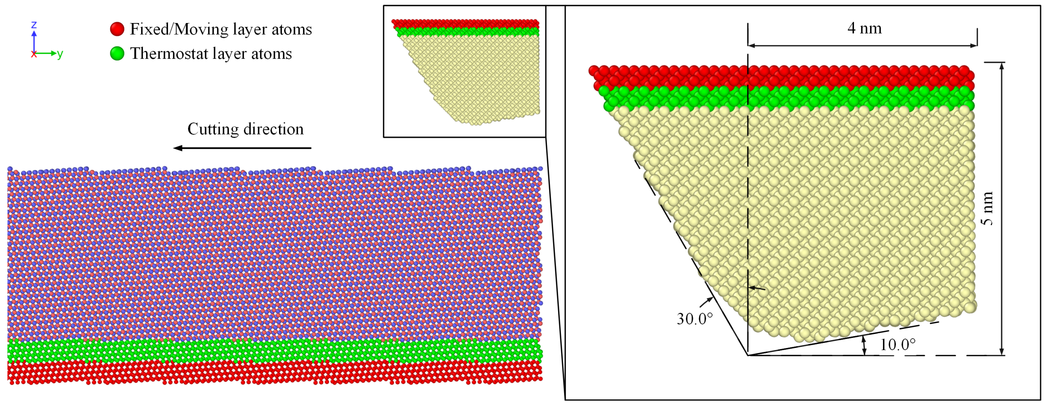
2. Models and Methods

The molecular-dynamics simulations in this paper were conducted with open-source software Large-scale Atomic/Molecular Massively Parallel Simulator (LAMMPS) [11]. The Tersoff potential [12] was adopted to describe the interatomic interactions in the SiC workpiece and the diamond cutting tool. The Morse potential [9] was adopted to describe the interatomic interaction between the SiC workpiece and the diamond cutting tool. Simulation results were visualized with Open Visualization Tool (OVITO) [13]. The identify diamond structure module [14] in OVITO was used to analyze the structure transformation and inspect the defect propagation in the SiC workpiece.
Figure 1 shows the nanocutting MD model of the off-axis 4H-SiC. The model consists of two parts, the diamond cutting tool and the SiC workpiece. The primary geometry parameters of the cutting tool are also shown in Figure 1. The cutting tool with a −30 rake angle and a 10 clearance angle was used in this paper. Since the hardness of SiC is comparable with a diamond, the cutting tool was not treated as a rigid body [7]. The atoms marked in red in the SiC workpiece are the fixed layer atoms, which provide mechanical support for the workpiece to prevent it from translation motion. The red atoms in the cutting tool are the moving layer atoms that drive the cutting tool moving at a constant speed. The atoms in green are the thermostat layer atoms, which prevent the workpiece and cutting tool from melting. The Nose–Hoover thermostat method was applied. The thickness of the fixed and thermostat layers in the SiC workpiece was 1.0 nm for both, and the thickness of the moving and thermostat layers in the cutting tool was 0.35 nm for both. Periodic boundary conditions were applied in the directions of x- and y-axis. Figure 2 shows three different workpiece models used in the simulations. Figure 2b is the on-axis SiC model. The lattice directions were [11−20], [−1100] and [0001] along the positive x-axis, positive y-axis, and positive z-axis, respectively. The typical off-axis angles are 4 and 8 . We chose a 4 off-axis angle in this paper, since a low off-axis angle is preferable to reduce cost, especially for large wafers. Figure 2a is the off-axis SiC model, where the c-axis rotates 4 toward [1−100]. Figure 2c is the off-axis SiC model, where the c-axis rotates 4 toward [−1100]. These models were used to investigate the influence of lattice orientation on nanocutting. Other parameters used in the simulations are listed in Table 1.
The simulation started with the equilibrium of the system at 300 K for 10 ns. Then, the cutting tool moving along the negative z-axis pressed into the workpiece. Finally, the cutting tool moving along the negative y-axis direction finished the cutting process.

3. Results and Discussion

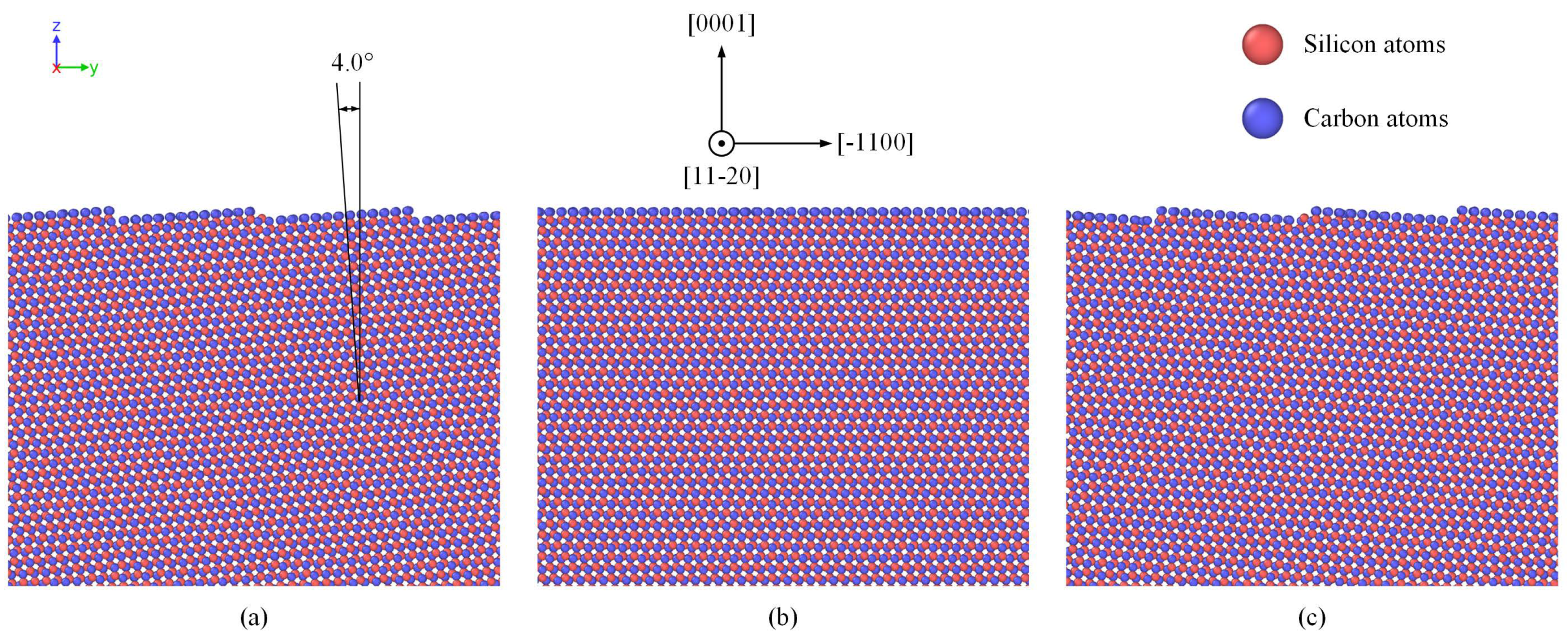
3.1. Influence of Lattice Orientation

3.1.1. Structure

Figure 3 shows the coordinate number of the 4H-SiC workpiece after cutting corresponding to Figure 2a. Cutting speed was 100 m/s, and cutting depth was 1 nm. They are the default cutting parameters unless otherwise stated. Atoms with a coordinate number larger than three were removed. It can be seen that the defect propagates into the workpiece at an angle, and most of the atoms with the coordinate number less than three are located on the surface. The atoms in green and blue on the surface not being fully bonded indicates that these atoms were in amorphous phase after cutting.
Figure 4 shows the structure transformation of three 4H-SiC workpiece models after cutting. Figure 4a–c correspond to Figure 2a–c, respectively. There are seven kinds of structure types in the workpiece. The atoms with an unidentified structure type were classified as “others”. Most of them were in the amorphous phase. The atoms with a cubic diamond structure and the ones with a hexagonal diamond structure were classified as “cubic diamond” and “hexagonal diamond”, respectively. The atoms being a first neighbor of a “cubic diamond” atom were classified as “cubic diamond (1st neighbor)”. Other structure types were defined in a similar way. It can be seen that defects all propagated in the basal plane. The defect in Figure 4a propagated deeper than the rest, and the defect in Figure 4c stopped propagating on the surface. Figure 5 presents the structures transformation in the defect region of three models after cutting. Figure 5a–c correspond to Figure 2a–c, respectively. The dashed line is the slip plane, and the yellow stick is the displacement vector. It can be seen that the atoms in the on-axis SiC model above the slip plane moved downward due to the compression, except the carbon atoms near the slip plane. The stacking sequence of Si was changed from -ABAC- to -ABBA- due to shear stress, which indicates that the defect in the basal plane is a stacking fault. The Si–C bonds crossing the slip plane were broken, and Si–Si bonds were formed after cutting. The stacking fault in the basal plane and the bond reconstrcution were also found in the off-axis models. The difference is that the stacking sequence in the off-axis models was changed from -ABCB- to -ABBA-, which means the atoms above the slip plane in the off-axis models moved twice as long than that in the on-axis model.

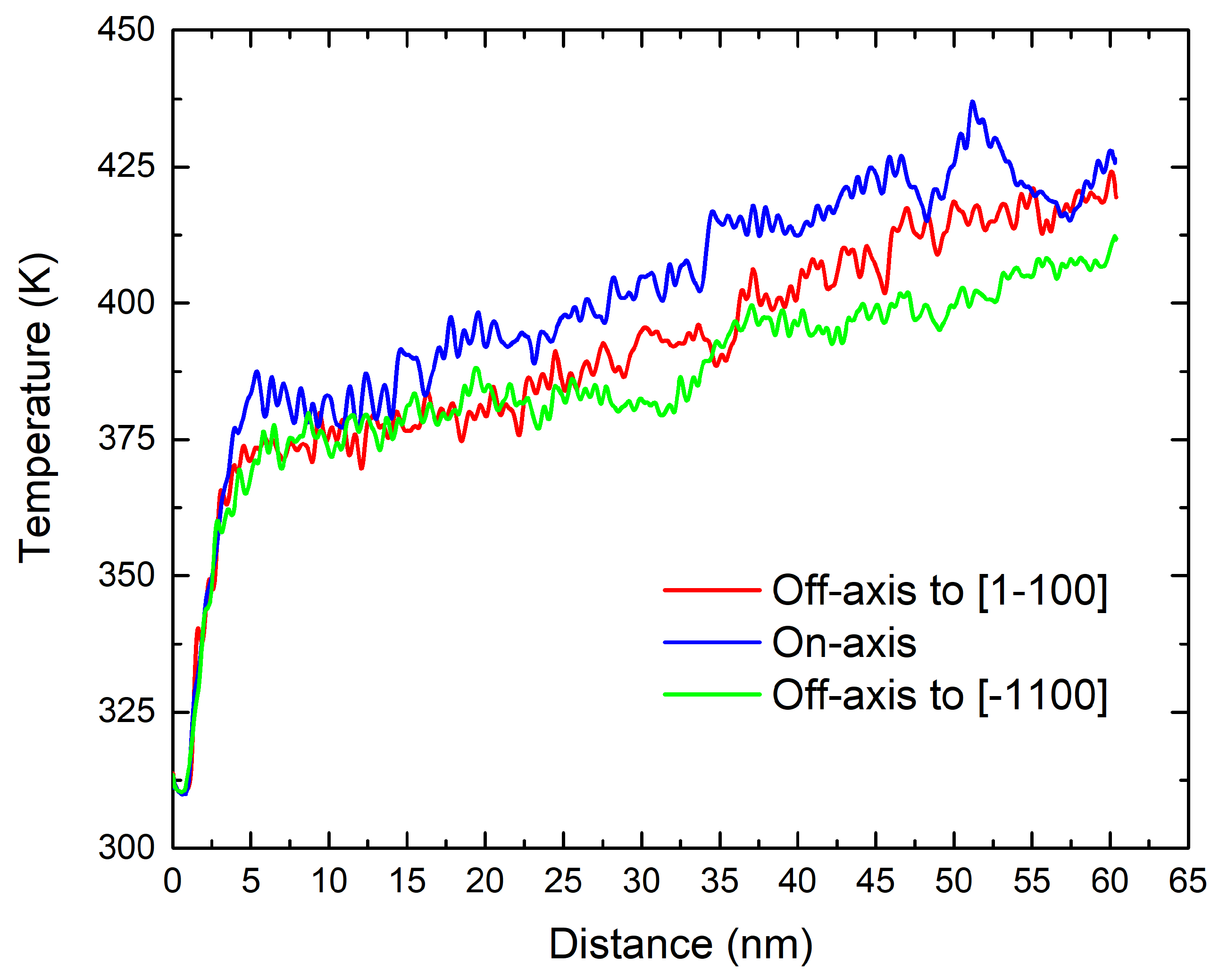
3.1.2. Cutting Force and Workpiece Temperature

Figure 6 shows the tangential and normal forces of the cutting with different lattice orientations. Tangential force is the component of a cutting force parallel to the xy-plane, and normal force is the z-component of the cutting force. Tangential force increases rapidly at the beginning of cutting, and then it grows with fluctuations as chip forms. The sudden decrease in the tangential force of on-axis model is marked with a circle. It is induced by the structure transformation on the surface of the on-axis model. Normal force decreases at the beginning and then increases with the cutting tool moving forward. The peak in the normal force of the off-axis model corresponding to Figure 4c is marked with a circle. As the defect propagates to the surface, normal force increases gradually. It decreased when the defect vanished on the surface. Figure 7 shows the temperature of SiC workpieces with different lattice orientations during cutting. The temperature of the on-axis model was slightly higher than the rest. Due to the absence of surface steps, more atoms were involved in the cutting of the on-axis model.
Lattice orientation has an impact on the 4H-SiC structure after cutting. Defects in the three models were all found in the basal plane. This is identical to the observation in the experiment conducted by Demenet et al. [15]. The defects were identified as stacking faults, and bond reconstruction was found in the vicinity of the slip plane. Since defects propagate along the basal plane, the behavior of the defects depends on the angle between cutting direction and the c-axis. When the angle is smaller than 90 , defects propagate deep into the workpiece. When the angle is larger than 90 , defects propagate to the surface. To control the quality of the SiC substrate, the angle greater or equal to 90 is preferred. However, it is impossible to control this angle during substrate thinning in practice because the grinding pad and the substrate are both rotating. Cutting force and temperature are also affected by the lattice orientation, while the effects are limited. The cutting force is sensitive to the structure trasformation. Tangential force and normal force are decreased when the atoms beneath the cutting tool are changed to amorphous phase. The cutting tool accumulates and releases energy through elastic deformation, which accounts for the fluctuation of the cutting force.

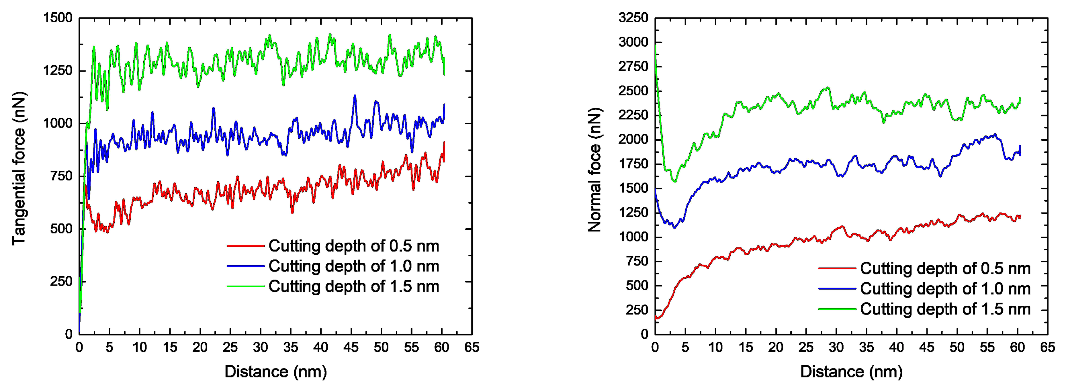
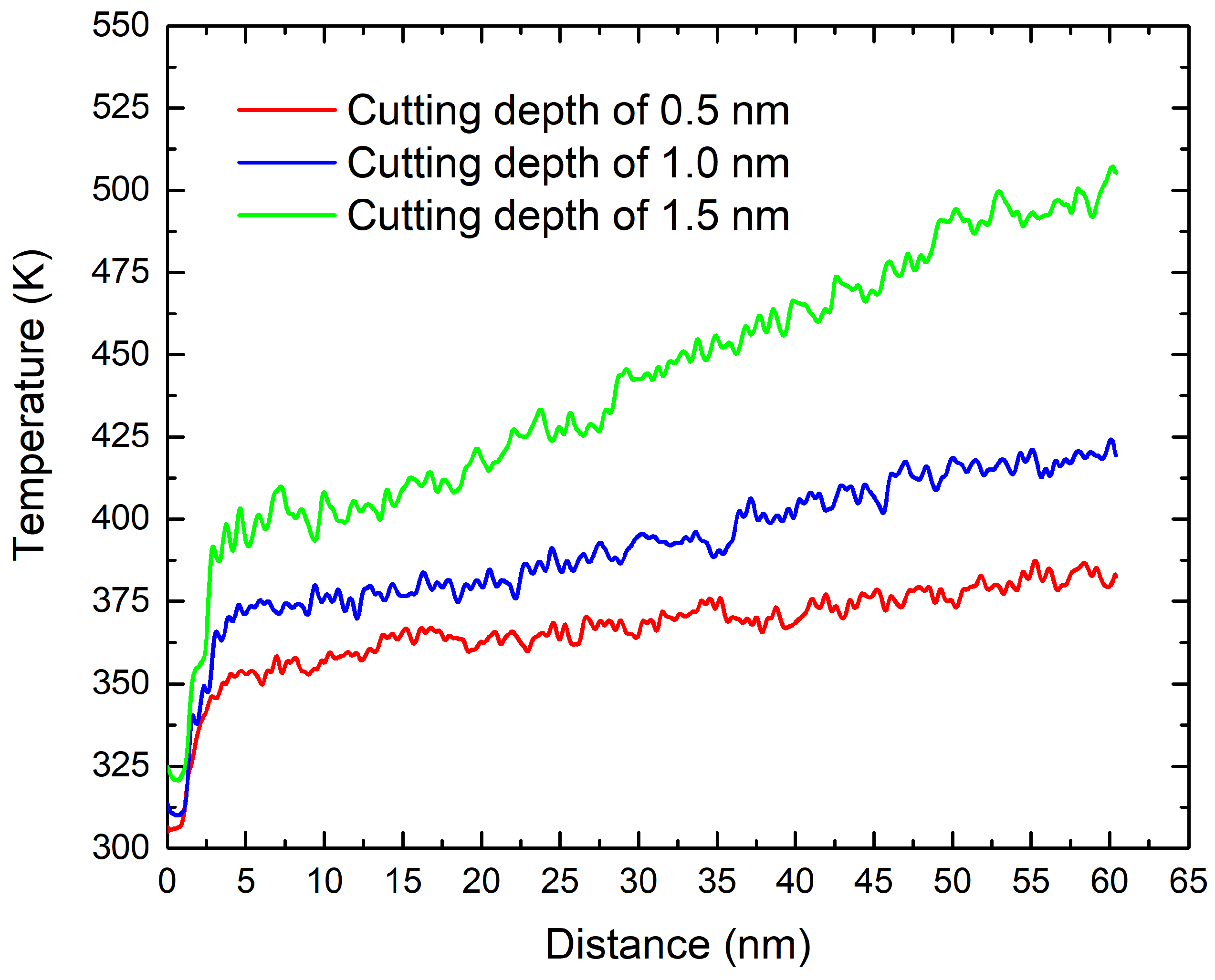
3.2. Influence of Cutting Depth
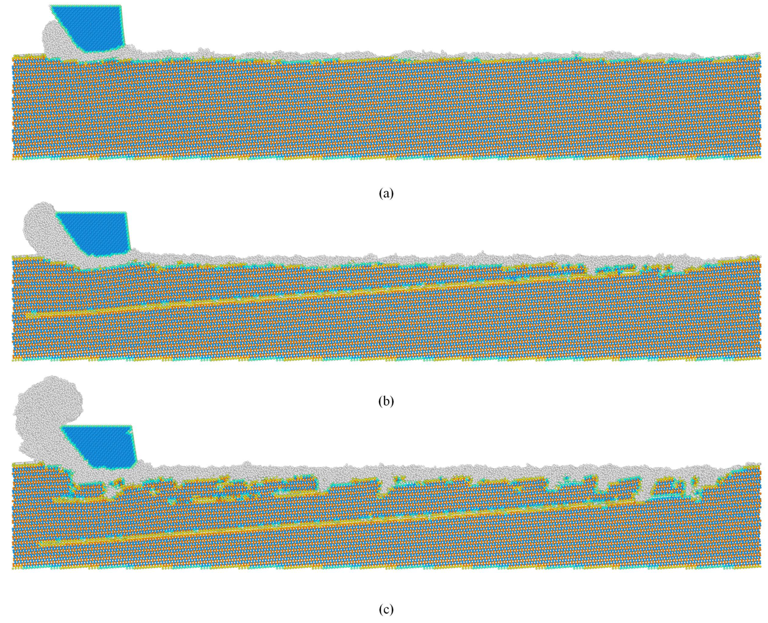
3.2.1. Structure

Figure 8a–c present the structure transformation of the off-axis 4H-SiC workpiece after cutting with a cutting depth of 0.5, 1.0, and 1.5 nm respectively. Atoms on the surface are changed into amorphous phase. With a larger cutting depth, more atoms are changed and material remove rate is higher. It can be seen that there is no defect in the workpiece in Figure 8a. The number of defects in Figure 8c was also more than that in Figure 8b. The deepest defect in Figure 8c almost reached the thermostat layer. The quality of the substrate was worse when cutting depth was larger.

3.2.2. Cutting Force and Workpiece Temperature

Figure 9 shows the tangential force and normal force during cutting with different cutting depths. The tangential force increases with the increase of the cutting depth. Tangential force with a cutting depth of 0.5 nm increased rapidly at the beginning, and then suddenly decreases. The normal force with the cutting depth of 0.5 nm increases at the beginning, unlike the rest. Normal force grew gradually with the chip forming beneath the cutting tool if the atoms beneath the cutting tool are not heavily distorted. Figure 10 shows the temperature of the 4H-SiC workpiece during cutting with different cutting depths. The temperature also increases with the increase of the cutting depth, as more atoms are chipped off when cutting depth is larger. The temperature of the workpiece with a cutting depth of 0.5 and 1.0 nm grew linearly durning cutting, while the slope of the temperature with a cutting depth of 1.5 nm became larger after 20 nm.
Cutting depth has a significant impact on the 4H-SiC structure during cutting. With a larger cutting depth, more atoms on the surface are changed to amorphous phase, and larger chip is formed in the front of cutting tool. The process is more like scratching than cutting, and no defect exists in the workpiece when the cutting depth is small. When the cutting depth is larger, the material remove rate is higher, and more defects exist. There is a trade-off between the efficiency and the quality. The cutting force and the temperature are also sensitive to the cutting depth. More atoms are involved in the cutting, which leads to the increases of force and temperature. Since the simulation region is adiabatic, if we ignore the energy variation induced by the structure transformation, the increment of the temperature can be described as:
Δ T = F V Δ t P Δ t 3 / 2 N k
where F is the tangential force, V is cutting speed, P is cooling capacity, N is the number of atoms, and k is the Boltzmann constant. When the tangential force is constant, the increment of the temperature is linearly correlated to the increment of time. As temperature is computed with the velocity of atoms, the rotation and the translation of the chip would induce workpiece temperature bias. Large temperature bias results in the slope increase of temperature.

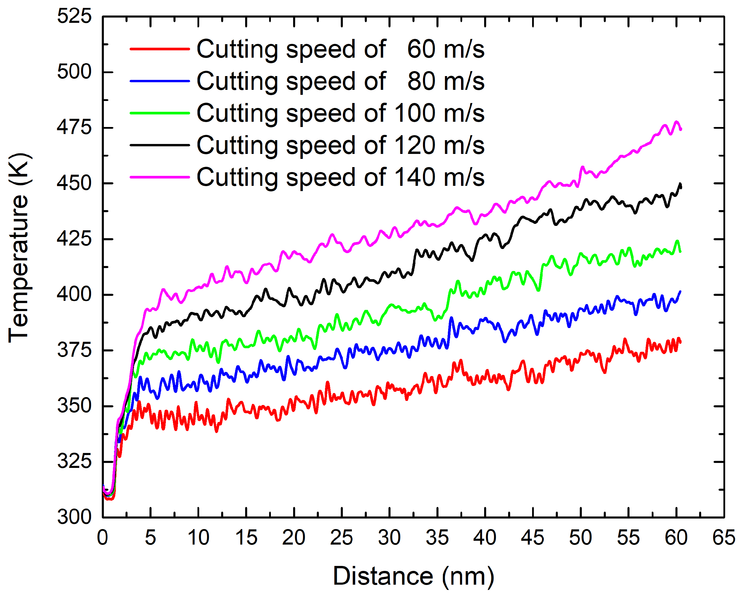
3.3. Influence of Cutting Speed

The temperature of the off-axis 4H-SiC workpiece during cutting with different cutting speeds is presented in Figure 11. It can be seen that the temperature of the 4H-SiC workpiece increases with the increase of the cutting speed. The larger the cutting speed is, the fewer the time costs and the less the heat dissipates. And it results in the increases the workpiece temperature. The effect of the cutting speed on the workpiece temperature is evident, while the effect on the structure transformation and the cutting force isn’t. The cutting speed may affect structure transformation and cutting force through temperature. However, the simulation time was relatively small (about 600 picoseconds) and the effects were not captured.

4. Conclusions

In this paper, the nanomachining characteristics of off-axis 4H-SiC have been investigated by molecular dynamics. Different off-axis MD models were built. The influence of lattice orientation, cutting depth, and cutting speed was investigated. A defect was induced by cutting propagates in the basal plane, and it was identified as a stacking fault. Bond reconstruction was also detected near the slip plane. If the angle between the cutting direction and the c-axis was smaller than 90 , the defect propagates deep into the workpiece. Cutting depth had significant impact on structure transformation, cutting force, and workpiece temperature. With a larger cutting depth, more defects were induced by cutting. Cutting force and the workpiece temperature were also larger. To select an appropriate cutting depth, material removal rate and defects are the things to consider. The effect of cutting speed is mainly reflected in the workpiece temperature. The workpiece temperature increases with the increase of the cutting speed. And it may further affect the structure transformation and the cutting force. Through this work, we aimed to reveal the machining characteristics of off-axis 4H-SiC and provide suggestions on SiC substrate thinning.

Author Contributions

Conceptualization, F.Z. and S.L.; methodology, M.W.; formal analysis, M.W. and Y.X.; investigation, M.W. and Y.X.; writing—original draft preparation, M.W.; funding acquisition, F.Z.

Funding

This work was supported by the 973 project (Number: 2015CB057203) and the National Natural Science Foundation of China (Number: 51675211).

Conflicts of Interest

The authors declare no conflict of interest.

References

  1. Lebedev, A.A. Deep level centers in silicon carbide: A review. Semiconductors 1999, 33, 107–130. [Google Scholar] [CrossRef]
  2. Wright, N.G.; Horsfall, A.B.; Vassilevski, K. Prospects for SiC electronics and sensors. Mater. Today 2008, 11, 16–21. [Google Scholar] [CrossRef]
  3. Matsunami, H. Current SiC technology for power electronic devices beyond Si. Microelectron. Eng. 2006, 83, 2–4. [Google Scholar] [CrossRef]
  4. Patten, J.; Gao, W.; Yasuto, K. Ductile Regime Nanomachining of Single-Crystal Silicon Carbide. J. Manuf. Sci. Eng. 2004, 127, 522–532. [Google Scholar] [CrossRef]
  5. Goel, S.; Luo, X.; Comley, P.; Reuben, R.L.; Cox, A. Brittle–ductile transition during diamond turning of single crystal silicon carbide. Int. J. Mach. Tools Manuf. 2013, 65, 15–21. [Google Scholar] [CrossRef] [Green Version]
  6. Goel, S. The current understanding on the diamond machining of silicon carbide. J. Phys. D Appl. Phys. 2014, 47, 243001. [Google Scholar] [CrossRef] [Green Version]
  7. Tanaka, H.; Shimada, S. Damage-free machining of monocrystalline silicon carbide. CIRP Ann. 2013, 62, 55–58. [Google Scholar] [CrossRef]
  8. Luo, X.; Goel, S.; Reuben, R.L. A quantitative assessment of nanometric machinability of major polytypes of single crystal silicon carbide. J. Eur. Ceram. Soc. 2012, 32, 3423–3434. [Google Scholar] [CrossRef] [Green Version]
  9. Wu, Z.; Liu, W.; Zhang, L. Revealing the deformation mechanisms of 6H-silicon carbide under nano-cutting. Comput. Mater. Sci. 2017, 137, 282–288. [Google Scholar] [CrossRef]
  10. Liu, Y.; Li, B.; Kong, L. Molecular dynamics simulation of silicon carbide nanoscale material removal behavior. Ceram. Int. 2018, 44, 11910–11913. [Google Scholar] [CrossRef]
  11. Plimpton, S. Fast Parallel Algorithms for Short-Range Molecular Dynamics. J. Comput. Phys. 1995, 117, 1–19. [Google Scholar] [CrossRef] [Green Version]
  12. Tersoff, J. Modeling solid-state chemistry: Interatomic potentials for multicomponent systems. Phys. Rev. B 1989, 39, 5566–5568. [Google Scholar] [CrossRef]
  13. Stukowski, A. Visualization and analysis of atomistic simulation data with OVITO–the Open Visualization Tool. Model. Simul. Mater. Sci. Eng. 2010, 18, 015012. [Google Scholar] [CrossRef]
  14. Maras, E.; Trushin, O.; Stukowski, A.; Ala-Nissila, T.; Jónsson, H. Global transition path search for dislocation formation in Ge on Si(001). Comput. Phys. Commun. 2016, 205, 13–21. [Google Scholar] [CrossRef] [Green Version]
  15. Demenet, J.L.; Amer, M.; Tromas, C.; Eyidi, D.; Rabier, J. Dislocations in 4H- and 3C-SiC single crystals in the brittle regime. Phys. Status Solidi C 2012, 10, 64–67. [Google Scholar] [CrossRef]
Figure 1. Nanocutting molecular-dynamics (MD) model of off-axis 4H-SiC.
Applsci 08 02380 g001
Figure 2. Three different silicon carbide (SiC) workpiece models. (a) 4 Off-axis toward [1−100]. (b) On-axis. (c) 4 Off-axis toward [−1100].
Applsci 08 02380 g002
Figure 3. Coordinate number of the workpiece after cutting.
Applsci 08 02380 g003
Figure 4. Structure transformation of three workpiece models after cutting: (a) 4 off-axis toward [1−100]; (b) on-axis; (c) 4 off-axis toward [−1100].
Applsci 08 02380 g004
Figure 5. Structure transformation in the defect region after cutting: (a) 4 off-axis toward [1−100]; (b) on-axis; (c) 4 off-axis toward [−1100].
Applsci 08 02380 g005
Figure 6. Tangential force and normal force of the cutting with different lattice orientations.
Applsci 08 02380 g006
Figure 7. Workpiece temperature of the cutting with different lattice orientations.
Applsci 08 02380 g007
Figure 8. Structure transformation of the workpiece after cutting with different cutting depths. (a) Cutting depth of 0.5 nm. (b) Cutting depth of 1.0 nm. (c) Cutting depth of 1.5 nm.
Applsci 08 02380 g008
Figure 9. Tangential force and normal force of the cutting with different cutting depths.
Applsci 08 02380 g009
Figure 10. Workpiece temperature of the cutting with different cutting depths.
Applsci 08 02380 g010
Figure 11. Workpiece temperature of cutting with different cutting speeds.
Applsci 08 02380 g011
Table 1. Parameters used in the simulations.
Dimensions4.6 × 70.2 × 10.0 nm (on-axis), 4.6 × 70.4 × 10.0 nm (off-axis)
Cutting speed60, 80, 100, 120, and 140 m/s
Cutting depth0.5, 1.0, and 1.5 nm
Cutting direction[1−100]
Time step0.5 fs

