Article

Direct-Write Dewetting of High Melting Temperature Metals on Flexible Substrates

ESRG, Department of Materials Science and Engineering, Rutgers, The State University of New Jersey, North Brunswick, NJ 08902, USA
*
Authors to whom correspondence should be addressed.
Appl. Sci. 2019, 9(15), 3165; https://doi.org/10.3390/app9153165
Submission received: 11 June 2019 / Revised: 27 July 2019 / Accepted: 30 July 2019 / Published: 3 August 2019

Abstract

:

Featured Application

Potential application in flexible microfluidics or MEMS sensors.

Abstract

Microelectromechanical systems (MEMS) are pervasive in modern technology due to their reliability, small foot print, and versatility of function. While many of the manufacturing techniques for MEMS devices stem from integrated circuit (IC) manufacturing, the wide range of designs necessitates more varied processing techniques. Here, new details of a scanning laser based direct-write dewetting technique are presented as an expansion of previous demonstrations. For the first time, the ability to pattern a high melting temperature and high reflectance metallic thin films of Ni and Ag, respectively, on polymer substrates is reported. Novel methods for reducing the power necessary for processing highly reflective films are demonstrated by depositing very thin films of high near-infrared absorbance.

Graphical Abstract

1. Introduction

Microelectromechanical systems (MEMS) and microfluidic devices encompass a great variety of physical designs. As such, the patterning processes utilized in MEMS fabrication must be equally as varied and versatile, expanding to frontiers beyond restrictive techniques such as traditional lithography. A great deal of research has been conducted regarding the dewetting of micro-scale thin films or nano-scale ultra-thin films because of the potential to create both periodic and free-form film structures without the need for complicated deposition, masking, and etching protocols. Moreover, dewetting may allow for a greater utilization of deposited material and can be used to impose periodic structures at small length scales at the expense of a precise control of geometry. Beyond the basic, randomized dewetting regimes that exhibit thickness-dependent periodicities [1,2,3,4], a number of researchers have conducted studies on methods to impose user-defined length scales and spatial ordering to the dewetting events. Such imposed spatial ordering can be achieved via probe-assisted perturbations [5], stamp generated dewetting [6,7,8], pre-patterned surfaces [9,10], and a number of other methods.
Dewetting of a liquid film occurs when the spreading pressure of a film (as determined by the surface tensions in the system) is overcome by the long-range intermolecular forces. The point at which a thin liquid film may spontaneously dewet is dependent upon the critical height, as shown in Equation (1), where λ is the capillary length and θe is the equilibrium contact angle of the liquid on the solid. In this regime, films may be metastable or unstable [11]. Dewetting then proceeds via two mechanisms: nucleation and the growth of holes, or spinodal dewetting. The former case may be triggered by defects in the substrate, while the latter case is characterized by the increased amplitude of capillary waves within the film. Solid metallic thin films are metastable depending on the choice of substrate and will often require additional energetic input before dewetting is observed [12]. This can involve raising the system temperature past the melting point of the metal; however, dewetting has also been observed in films while they were in the solid phase and at room temperature (~20 °C) [13,14,15]. Past studies have shown that the dewetting of metallic films can be induced by the use of a laser input from both defocused and focused sources [16,17,18].
h c = 2 λ sin θ e 2
The use of a laser opens the possibility of a rastered laser to develop dewetted structures that may be “written” on demand. Singer et al. recently demonstrated that a focused 532 nm laser radiation can be used in conjunction with an X-Y movement stage to create dewetted polymer structures of polystyrene films deposited upon a silicon substrate [19]. In parallel, our group has demonstrated the direct-write patterning and structure formation of low melting point metal films on polymer substrates by using a high speed scanning laser [20]. Recently, Oh et al. have detailed a similar technique for plasmonic color printing on glass [21].
More specifically to our initial work, low melting temperature bismuth and tin films deposited upon Parylene-C (Par-C) coated glass slides were patterned using a focused 1060 nm laser and high-speed galvanometer scan system. During the irradiation process, the films experienced a localized dewetting event that was initiated by melting and thermocapillary flow in the heated area. As the laser heated the target area, a thermal gradient formed beginning at the center of the focal point and radiating outward. A concurrent and parallel surface tension gradient forms in this area due to the variation of the surface tension with the temperature. This results in Marangoni flow away from the center and outward.
The process is diagramed by Figure 1, where the dewetting event is separated into three main regions: heating, thermocapillary flow, and hole growth. The choice of laser wavelength, flux density, target material, and substrate material all play a large role in the viability of this technique to effectively create dewetted structures without damaging the underlying substrate. This is of particular importance when using polymer substrates with metal targets, since the melting point of the metal film is so high.
In our previous examples of the direct-write dewetting of metals, the film targets were characterized by a relatively high absorptivity in the near-infrared range and melting points comparable to the softening/degradation points of polymers such as polytetrafluoroethylene (PTFE), polyimide (PI), and Par-C. Many of these polymers are used in the micro-electronics and MEMS industries for their mechanical flexibility, high temperature thresholds, and their barrier properties [22,23,24]. For applications that require a greater degree of thermal conductivity, electrical conductivity, bio-compatibility or heat resistance than low Tm materials such as Bi or Sn can provide, it is more practical to use thin film compositions involving metals such as Ni, Au, Ag, or Cr. Our group has shown that layered substrates of Par-C deposited upon borosilicate glass are not damaged by near-infrared laser radiation light at relevant processing intensities [20]. Thus, they represent a viable choice in further investigations, especially in conjunction with their excellent biocompatibility for implantable micro electrode arrays [25,26]. With a melting point of 1455 °C, nickel’s thermal, electrical, and optical properties (Table 1) are typical of the Group VIIIB elements. Nickel thin films have been used in sensors [27] and electrochemical cells [28], and they exhibit a relatively high absorptivity in the NIR range. Conversely, Group IB elements, such as silver, are characterized by a relatively low absorptivity in the NIR range, while boasting the highest thermal and electrical conductivities of the transition metals. Nickel and silver films are representative of the extremes in high melting point and reflectivity, respectively, which are of a particular challenge to the laser dewetting on polymer substrates. Developing the direct-write dewetting of these two metals will prove essential to the progression of the technique to a wide variety of additional metals. In this regard, the effects of the higher melting temperatures were investigated with respect to any possible damage to the underlying substrate. Additionally, layered films were studied as a means to enhance the effects of NIR laser radiation and to bypass the high reflectivity of the silver thin films.

2. Materials and Methods

Pre-cleaned borosilicate glass microscope slides were coated with a 22 μm thick layer of Par-C via CVD methods, as previously described [20]. These coated slides served as substrates for a number of single and multi-layered metal films. Ni films were sputtered at thicknesses of 320 nm and 640 nm. Ag films were evaporated onto the described substrates at a thickness of 405 nm. Multi-layered films were created by evaporating 45 nm of Bi onto 405 nm of Ag. Additional multi-layered films were created by sputtering 45 nm of Ni onto 405 nm of Ag.
All film processing was conducted with an integrated laser processing system consisting of a near-infrared (NIR) laser (SPI redPOWER R4-HS), an in-line camera system (uEye GigE), a galvanometer-driven scanner (Scanlab IntelliSCAN 20) with an f-theta telecentric lens (115 mm effective focal length) and a custom-made sample stage. The sample stage allowed for the manual adjustment of the z-axis as well as tilt-leveling around the x- and y-axis. The telecentric optics ensured a consistent laser intensity through a flat focal plane. Laser exposure was conducted in both the pulsed-mode and in the continuous-wave exposure, depending on the chemistry of the target film and substrate. While in the pulsed-mode, the laser ran at 10 W, with pulse lengths of 2.5 μs and an exposure frequency of 100 kHz. The beam waist was ~34 μm in diameter under these conditions, as calculated by Equation (2), where M2 is the beam quality factor (< 1.1), λ is the wavelength (1060 nm), f is the effective focal length (115 mm), ri is the beam radius as it enters the lens (2.535 mm), and r0 is the radius of the beam at the focal point.
r 0 = M 2 λ f π r i
With this beam spot, the processing parameters resulted in a pulse fluence of 2.75 J/cm2. At speeds of 0.2 m/s, the normalized scan energy was calculated to be 12.5 J per meter scanned. Under a continuous wave (CW) operation, scan speeds were increased an order of magnitude to 2.0 m/s to compensate for the lack of cooling between the pulses. With an output power of 25 W, the normalized scan energy remained at 12.5 J per meter scanned for the CW operation, but retained higher laser intensities to overcome high reflectivity barriers, such as in the case of Ag films. Layered films were dewetted with a laser power of 10 W and speeds of 1 m/s and 3 m/s, which resulted in scan energies of 10 J and 3.33 J per scanned meter, respectively.

3. Results

3.1. Directed-Dewetting of Ni and Ag on Par-C Substrates

3.1.1. Nickel

A typical set of metallic lines fabricated from 640 nm Ni thin films on Par-C substrates are pictured in Figure 2. Examples of similar Ni films deposited to only 320 nm onto borosilicate glass or Par-C can be found in Figure S1 of the Supplementary Material. 100 µm and 40 µm pitch lengths were scanned into the films revealing dewetted trenches and bordering ridges as a result of the movement of the molten metal along the polymer surface. Associated profilometry scans of the two sets of lines reveal the characteristic film-ridge-trench-ridge-film profile, similar to that observed in earlier studies focused on low-melting temperature metal films [20]. The low trenches represent the surface of Par-C exposed after the rastering laser induced complete dewetting of the molten Ni. The morphology of the ridges created by the displaced material located alongside the trenches parallel to the motion of the laser beam is, in large part, uniform; however, there are signs of a continued morphological evolution along the ridge into a series of beads.
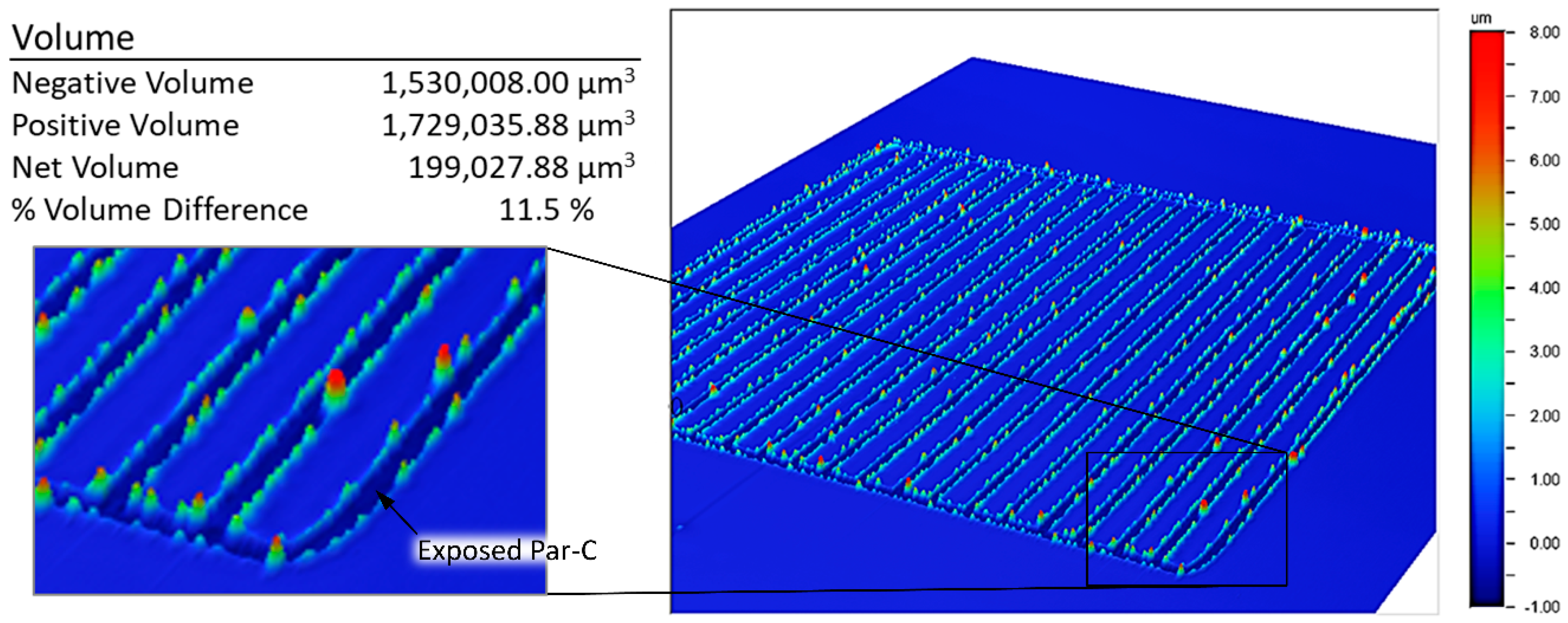
Three-dimensional mapping (Figure 3) of the linear structures provides evidence of Ni dewetting rather than ablation. Any material displaced above the baseline surface of the Ni film is tallied as a “positive” volume. The volume is then compared to the voids occurring below the baseline surface, which are tallied as a “negative” volume. For the 100 μm pitched array, only 11.5% of the positive volume remained unaccounted for, suggesting that the clear majority of the Ni film is conserved. The excess positive volume is most likely due to minor shadowing effects from the shape of the probe and the shape of the features, where the negative volume remains unmeasured.
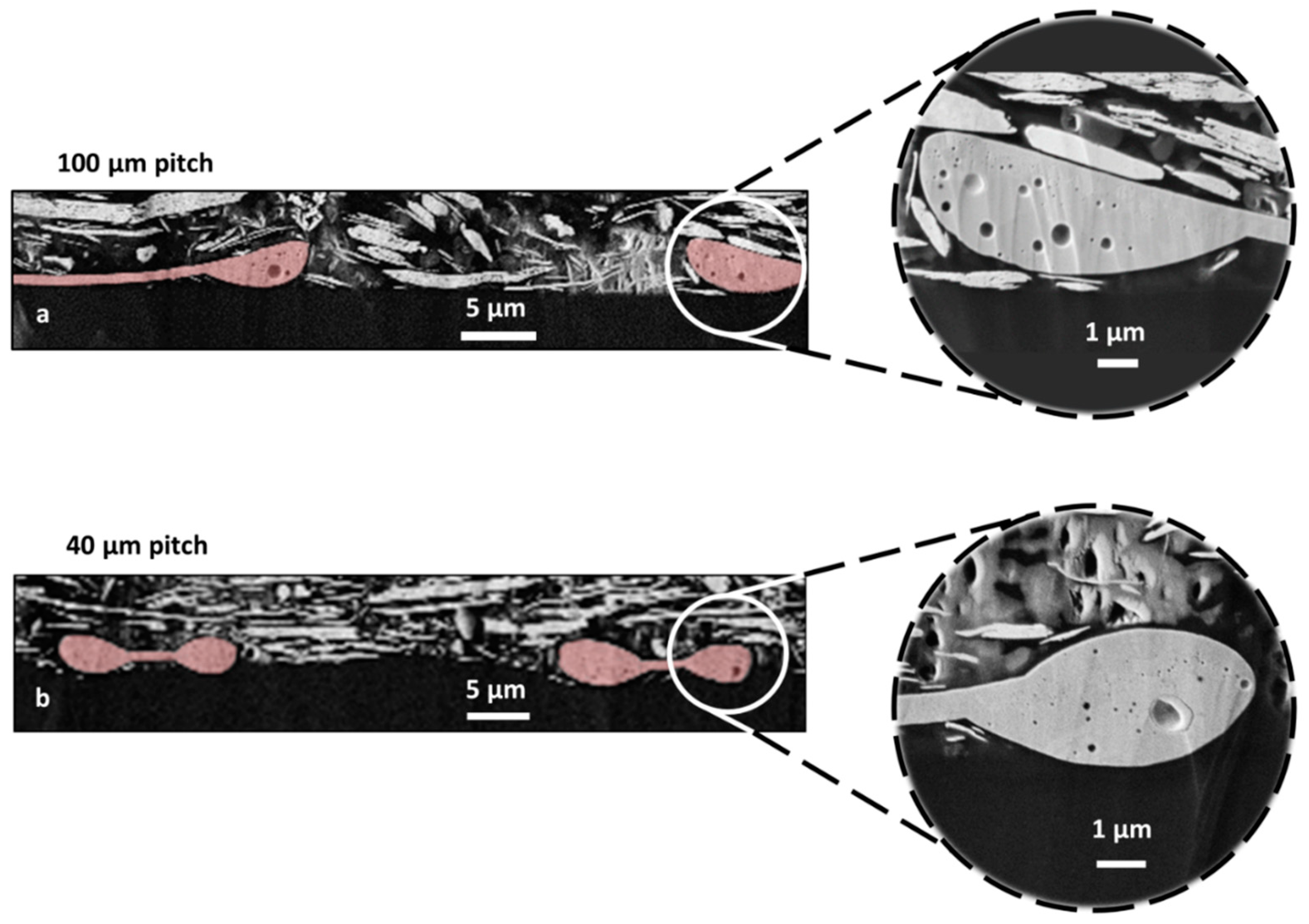
The evolution of the Ni films after dewetting were achieved by a FESEM analysis of Ar ion cross sectioned samples embedded in Ag epoxy. The FESEM analysis (Figure 4) of the 100 μm array reveals the evolution of the Ni films after the dewetting action. Each FESEM image displays an area of newly exposed substrate surrounded by an accumulation of the dewetted Ni material ridge, with no residual Ni present in the dewetted area. The reader is directed back to Figure 1 for a general schematic of the structure cross-section.
The solidification of the dewetted and displaced nickel occurs underneath the remaining film. The partial delamination of the film at the edge of the laser path can be observed in Figure 4a, but it is unclear whether the delamination occurs before or after the melting occurs. This results in bead formation underneath the film rather than on top—a sharp contrast to the morphology of other dewetting thin film examples [20,37]. No films other than the Ni films exhibited the same type of inverted dewetting, nor did any films exhibit delamination to the same extent. Other films containing some portion of Ni are discussed below, showing some delamination immediately adjacent to the laser path. As the pitch is lowered to 40 μm in Figure 4b, the dewetted bead becomes nearly symmetrical around the non-melted film to form a “dumbbell” cross-section created out of two adjacent laser scans. The unprocessed film in between the 40 µm pitch ridges is also delaminated and, due to the small pitch, it extends all the way across to the next ridge formation. The ridges themselves appear to stay adhered and reside in small indentations within the Par-C surface that were most likely created during the dewetting action. Both cross-sections also exhibit a sub-micron porosity formed in the ridges of the dewetted material. No other investigated material exhibited such a porosity. The voids that are observed in both sets of Ni linear arrays most likely arise from the degradation or outgassing of the polymer at the interface, as no voids are visible in the original, non-dewetted and displaced Ni film. The gas evolution from the surface of the polymer may play an important role by protecting the Par-C from the intense heat of melting Ni through the presence of a thermally insulating gas, similar in consequence to the Leidenfrost effect [38]. In addition, the gas formation may be responsible for the aforementioned “delamination” of the film from the surface prior to melting. In the future, it would be of interest to observe and possibly verify this process through an in-situ characterization.
To achieve well-defined dewetted structures in metal films deposited on polymer substrates, the preservation of the polymer substrate emerges as one of the major hurdles. This is especially true when processing high-melting point metal films. Par-C has a relatively low degradation temperature of 290 °C compared to the 1455 °C melting point of Ni; therefore, there is a large risk of substrate degradation during the dewetting process. While optical micrographs do not show any apparent charring or degradation within the exposed polymer, some deformation of the substrate surface may be expected due to the polymer’s thermoplastic behavior, in addition to the aforementioned evidence of surface vaporization.
Profilometry scans (Figure 2b) and cross-section micrographs (Figure 4b) on the 40 μm pitched array demonstrate the existence of deformation of the polymer surface via the wavy appearance in the trench area between the dewetted nickel ridges. Similar heat induced deformations are not observed in the profiles of the 100 μm pitched array (Figure 2a), likely due to a lower overall heat concentration and greater thermal conductivity of the larger remaining metal digits.
In the case of short-pitched laser scans, higher concentrations of heat accumulate, expose the Par-C to higher peak temperatures, and lead to the deformation observed in the 40 µm pitch vs. the 100 µm pitch. Increasing the wait time between the laser passes, or alternating the scans may provide a greater amount of cooling; however, a more effective solution would be to use a lower power setting beyond the capabilities of the present laser system.

3.1.2. Silver

Processing Ag films in a similar fashion to Ni also leads to a melt and dewet event. While Ag has a relatively high melting point (but lower than Ni), the challenges are exacerbated by the higher inherent reflectivity of Ag vs. Ni, (> 95% vs. < 75%, respectively) at a 1060 nm wavelength. In addition, Ag exhibits the highest thermal conductivity of all the metals. The latter is detrimental as higher laser flux densities are required for the initial melting, but also helpful as the heat-induced damage of the Par-C substrate will be decreased by the rapid expulsion of heat after dewetting. To compensate for the increased reflectivity and thermal conductivity, the laser was operated in a continuous wave mode at a power of 25 W, which delivered a higher incident intensity to the target film. The intensity overcame the reflectivity and allowed the melting and subsequent dewetting process to take place. The use of high-speed scanning prevented the destruction of the underlying polymer substrate. The morphology of the film and substrate after the dewetting event is displayed in Figure 5. While the gross destruction of the polymer substrate has been avoided, there are clear ripples within the exposed polymer substrate that extend out past the ridges formed from the dewetted material. The ripples are clear deformations of the Par-C, but it is unclear whether they form within the polymer first and transfer to the deposited metal film, or if the metal film contracts and forms the ripples during the rapid cooling associated with the laser processing.
As seen in Figure 2, the morphology of Ni films tends toward continuous or semi-continuous ridges along the length of the trench; however, the dewetted Ag films in Figure 5 show the formation of more distinct spheres—most likely due to a faster instability growth relative to the other films. Similar instabilities have been observed in the rims of dewetting holes in polymer films and are analogous to Plateau-Rayleigh instabilities [39,40,41]. As Choi and Newby pointed out in their investigations of such rim instabilities, their growth rate, q, is described using Equation (3).
q = γ m 6 R 0 μ l
where γm is the surface tension of the liquid, R0 is the radius of the hole formed, and μl is the viscosity of the liquid. The authors describe a positive correlation between the dynamic contact angle of the dewetting film and the growth rate of the perturbations. The observed contact angles of the dewetted Ag ridges ranged between 130° and 155°, which is in line with the high surface tension of Ag noted in Table 1. A similar analysis suggests that the growth rate of the instabilities is larger within the Ag film ridges than the rate exhibited by the Bi or Sn films when deposited upon Par-C [20]. The growth rate of the instability may be hastened by the high thermal conductivity of the Ag film. During scanning, there exists a thermal gradient both perpendicular and parallel to the direction of the scanning. Similar gradients have been studied during the high-speed welding of metal plates using a laser with beam qualities on par with the current system [42].
To prove that Ag was displaced, as opposed to being ablated, an accounting of the film volume was achieved using profilometry (Figure 6) in a similar way as shown for Ni (Figure 3). The accounting of the displaced volume (Figure 6) reveals that only 7.9% of the excess positive displaced volume is left unaccounted, proving a displacement via dewetting vs. that of an ablation process. The 7.9% discrepancy may be explained by small shadowing effects created by the aforementioned spherical accumulations along the dewetted Ag ridges, as well as the measurement variation of the profilometer and/or ablation of a small amount of Par-C.
The cross sections of the dewetted Ag digits are presented in Figure 7. Unlike the previously described Ni film, the dewetted ridges show no signs of porosity within the beads formed by the displaced material or film delamination. The absence of the pores may be a result of the lower melting point and higher thermal conductivity of the Ag relative to Ni, thus reducing the heat load on the underlying substrate and reducing vaporization at the metal-polymer interface. Furthermore, the increased thermal conductivity quickly dissipates the high heat concentration at the exposure point, leading to less substrate degradation. Like the pure Ni films, there is no visible destruction of the Par-C substrate—even in the face of a much higher laser intensity.
To avoid the high intensity operation needed to overcome the reflectivity of the Ag, Ag films were coated with a 45 nm absorption layer of Bi or Ni to lower their reflectivity. The adsorption layers were kept to 10% of the thickness of the base silver film. Line arrays with a 100 μm pitch were dewetted into both types of layered films. Initial dewetting trials were performed using a 50 kHz, 5 µs processing regime and scanned at various speeds. Figures S2 and S3 in the Supplementary Material provide examples of the different speeds used in the resulting edge qualities. By doubling the frequency and halving the pulse duration, the energy per meter values were kept the same, while also giving slightly better edge qualities. The cross-sectional FESEM images can be seen in Figure 8; the edge quality is featured in Figure 9. Similarities can be seen between the two types of layered films. Ridge formations appear to flatten and widen to a greater degree relative to the uncoated Ag films of Figure 7, but still exhibit larger cross-sectional heights compared to the original film height.
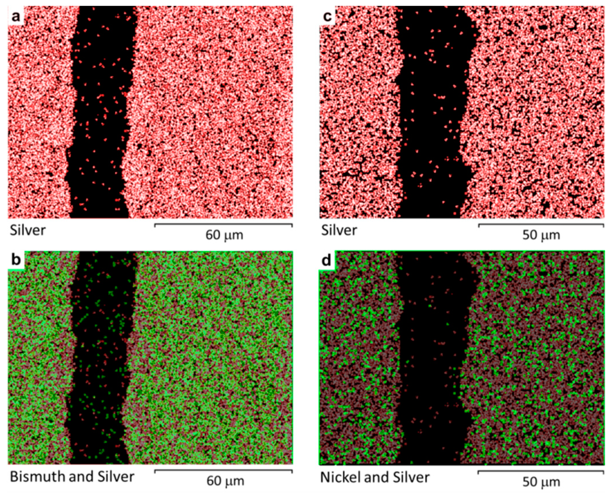
The metal films were characterized using energy dispersive x-ray spectroscopy (EDS) elemental maps to identify the distribution of the metals after dewetting. Figure 9 displays surface maps (top-down view) of the post-processed multi-layered films. For both films, there is evidence of a relatively uniform distribution of the absorption metal (Bi or Ni) among the Ag. Because of the penetration depth of approximately 1 μm of the EDS analysis, it is not possible to determine the surface vs. bulk distribution of the elements.
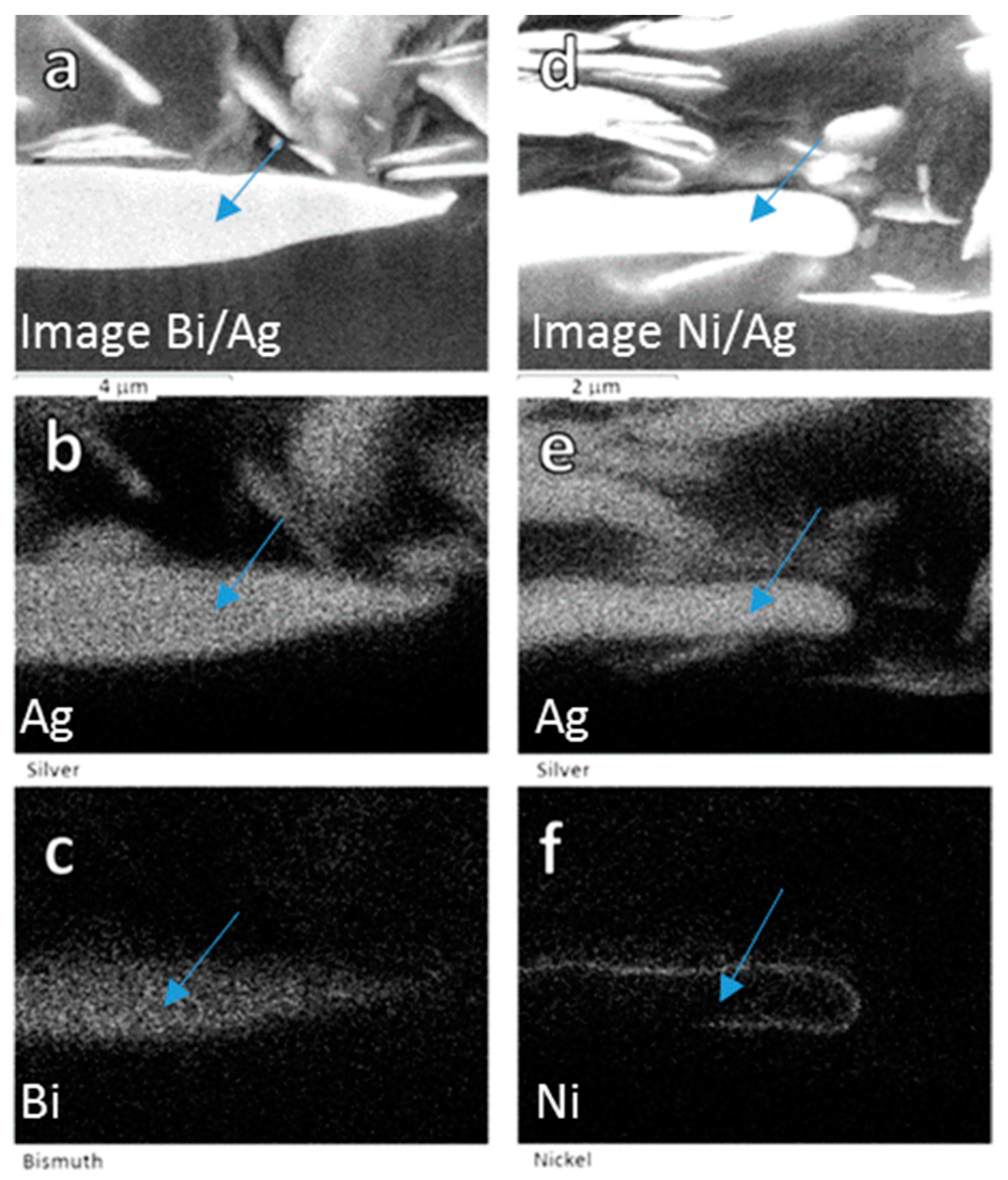
To verify the bulk distribution of the metals after the dewetting and subsequent displacement, similar EDS maps were performed on the cross sections of the metal displaced in the form of the “ridge”. In the case of the Bi-coated sample, the Bi top film is incorporated within the bulk of the displaced metal, as clearly seen in Figure 10c. The low Tm Bi film will melt first, and according to the phase diagram the Bi-Ag system exhibits a small degree of Bi solubility in Ag above 175 °C [43]. As the processing induces very fast cooling rates, it could be that a limited degree of Bi solubility in Ag occurs through super-cooling.
In sharp contrast to the Bi absorption layer scenario, when using the Ni absorption layer, the underlying Ag will tend to melt prior to any thermocapillary action of the Ni. Thus, we expect a movement of the Ag film without mixing of the Ni film. The EDS of the dewetted areas confirm our expectations. In general, we observe a mixing of Bi and Ag in Figure 10c, but with a significant phase segregation of Ni (Figure 10f). Ni is seen nearly encapsulating the Ag core structure of the displaced metal.
In both cases, the absorption film was a successful technique to lower the relatively high 12.5 J/m scan line energy required to dewet the highly reflective Ag films. The addition of the Bi NIR absorption film enables a decrease to 10 J/m, while the addition of a nickel NIR absorption film enabled a very significant decrease to 3.33 J/m. NIR absorption layers could enable 1060 nm processing of other highly reflective metals such as gold, aluminum, or copper, with a minimal change in the base composition. In addition, the results suggest that a coating of a high absorption film with a similar Tm to the high reflectance film would be optimal.

3.2. Complex Pattern Direct Dewetting of Ni and Ag Films

Ultimately, the advantage of using the scan-system in the dewetting process manifests in the ability to quickly fabricate complicated and free-form shapes, such as one would want for microelectrodes or microfluidic channels. To demonstrate such effectiveness, inter-digit electrode (IDE) pairs were both patterned into single-layer sets of films. By measuring the electronic resistivity between the two electrodes, we can characterize the extent to which dewetting occurs, while also demonstrating a moderately complex pattern design. Figure 11 presents an example of such an IDE created in Ag films. Each electrode was connected to 45 inter-digits, with 30 μm spacing and an 80 μm width. The spacing between the digits represents a single pass of the laser. The resistance within the unprocessed area was measured using an ohmmeter at various points throughout the film prior to processing to establish the film’s connectivity. After processing the film into the dewetted IDE, two-wire resistance measurements across the two electrode pads generated values > 1 G-Ohm. Therefore, it is concluded that the dewetting action proceeds completely and does not leave any percolated conductive metal or by-products. The EDS maps presented in Figure 9 also confirm the lack of any significant amount of residual metal within the trench area after processing. An inspection under an optical microscope and under SEM (Figure 11a) appeared to show that all the inter-digits were continuous; however, electrical conductivity was not confirmed via direct-measurement due to the small size of the features. The lift-off of the Par-C polymer substrate from the glass slide backbone produced an IDE patterned onto a flexible, free-standing polymer, as seen in Figure 11b,c.
The use of the scanner allowed for successively shifted, overlapping passes of the laser beam within a single pattern. This type of scanning induces a buildup of displaced metal along the dewetting front. Previous work on Bi and Sn thin films demonstrated that this buildup can be manipulated via different scanning geometries to produce structures many times thicker than the original deposited film [19]. Attempts to perform such “push” dewetting on Ni films were realized, but within certain limitations. Figure 12b diagrams the laser scanning procedure, where three scans are carried out with partial overlap in the specified numerical order. The thickness measurements (Figure 12a) demonstrate a designated preferential dewetting to one side of the exposure trenches. For example, a single laser pass across a 0.64 μm Ni film resulted in displaced Ni ridge heights ranging between 3.6 μm and 4.3 μm, while a multi-pass process will result in ridge heights between 5.3 μm and 7.1 μm, approximately 10X the value of the original Ni film thickness. A side effect of the pushing procedure manifests as a smoothing of the edge profile of the trench/ridge interface. This is most pronounced in Figure 12b, where the non-pushed edge appears slightly scalloped on the left, while the built-up edge at the end of the dewetting front on the right (boxed) presents as relatively smooth.

4. Discussion

The results have shown that it is possible to extend the thermocapillary directed dewetting technique beyond low-melting point metals to metallic films with very high melting points and a high reflectivity. Despite the high melting temperature of Ni and high reflectivity of Ag, dewetted features on polymer substrates are possible under scanned, near-infrared laser heating. Use of a powerful, single-mode laser with a high-beam quality remains essential for successful patterning, as the Gaussian spatial distribution of intensity drives the flow.
During the laser exposure of Ni and Ag films deposited on a Par-C substrate, a very thin polymer-vaporization layer likely forms at the metal-polymer interface. Although evidence was only observable in the extreme case of Ni, this may be a prevalent feature of many of the dewetting events and may indeed be a critical factor by providing thermal insulation at the metal-polymer interface during the process. While the specific heat of Par-C is approximately double that of Ni [35], the thermal conductivity of Par-C is three orders of magnitude lower than Ni (see Table 1), which may explain why the Par-C does not incur more damage while in contact with the dewetting metal. The thermoplastic effects that are seen, such as the deformation of the Par-C, indicate that there is a significant temperature rise at the interface between the plastic and metal layers; however, this is likely a function of the speed of dewetting. The laser can, in certain instances, impart more damage to the Par-C than the dewetting metal. This may occur if the processing speed is slowed down, thus allowing the metal layer to dewet and exposing the Par-C directly to the laser energy for an increasing amount of time. The processing settings must consider the temperature increase of the metal, the temperature increase of the Par-C, and the absorptivity of the metal layers. As such, this deserves further characterization.
In this study, thin absorption layers are shown to decrease the need for an exceptionally high average laser power output for highly reflective films such as Ag; however, the use of visible or ultraviolet laser radiation may offer another avenue for approach. Ag experiences an increase in theoretical absorptivity for wavelengths at the near-UV range to nearly 24%—a stark difference from the < 5% observed in the near-IR range. Wavelengths in the mid-UV range, such as those from a frequency quadrupled Nd:YAG laser (266 nm), are absorbed at a theoretical 75% and therefore would not require the high average power exerted by the current laser system. Shorter wavelength lasers would also allow for smaller ultimate spot sizes and thus higher resolution features with a more effective dewetting on thinner films. One drawback to using a UV laser source may manifest in the absorption properties of the polymer substrate and the subsequent damage. This technique is in its infancy; as such, the full range of processing parameters and material combinations is yet to be explored. The limits in the feature size and edge quality will have to be explored using various geometries, substrate roughness values, and materials choices. Still, the technique offers the possibility of creating structures of varied thicknesses without additional deposition coatings, masks, or etching steps. In some ways, this approach represents a micro-additive fabrication technique. Eventually, the technique may be used in conjunction with traditional lithographic processes, or perhaps in place of some.

5. Conclusions

It has been demonstrated that at a very high melting point, high reflectivity metals such as Ni and Ag, respectively, may be dewetted into patterns via a scanning laser beam on flexible polymer substrates. High average powers are used to quickly heat the target films to their melting point, after which the spatial variation of the laser beam will induce a thermocapillary flow away from the center point of exposure. Substrate destruction is avoided by using a polymer with high transmittance at the laser operating wavelength and fast scan rates of the laser. Metals with elevated reflectivity rates can be patterned using increased laser intensities or by depositing thin NIR absorption layers, thereby lowering the required flux intensity by over a factor of 2.
The use of the scan system allows for complex shapes to be dewetted into the metallic target layer to form patterned metallic films on flexible polymer substrates. Resistance measurements confirmed that a single pass of the laser leaves no connecting conductive material in the exposed area, thus ensuring electrically isolated features. Finally, by making partially overlapping passes, the dewetting high temperature metal can be “pushed” in a directional manner, which gives rise to thicker features without the need for additional deposition steps.

Supplementary Materials

The following are available online at https://www.mdpi.com/2076-3417/9/15/3165/s1, Figure S1: Ni films deposited to a thickness of (a) 320 nm on glass, (b) 320 nm on Par-C, and (c) 640 nm on Par-C. All lines processed using the laser at 10 W with 2.5 µs pulses at 100 kHz. Films on glass were scanned at 0.3 m/s while films on Par-C were scanned at 0.2 m/s. All features are created at a 50 µm line-to-line pitch. Figure S2: Bi-coated Ag films deposited on Par-C. Films were processed from the (a) “front” at 10 W where the Bi-film is directly exposed and from the (b) “back” at 40 W where the laser is routed through the glass and Par-C substrate to hit the Ag film directly bypassing the Bi film. Features are created using a 50 kHz, 5 µs regime and scanned at various speeds. Figure S3: Ni-coated Ag films deposited on Par-C. Films were processed from the (a) “front” at 20 W where the Ni-film is directly exposed and from the (b) “back” at 40 W where the laser is routed through the glass and Par-C substrate to hit the Ag film directly bypassing the Ni film. Features are created using a 50 kHz, 5 µs regime and scanned at various speeds.

Author Contributions

Conceptualization, G.G.A. and A.J.F.; methodology, A.J.F. and G.G.A.; formal analysis, A.J.F.; investigation, A.J.F. and A.H.; writing—original draft preparation, A.J.F. and G.G.A.; writing—review and editing, G.G.A. and A.J.F.; supervision and project administration, G.G.A.; funding acquisition, G.G.A.

Funding

This research was funded by the US Government.

Acknowledgments

The authors would like to thank John Gural and Barry Vaning for technical assistance.

Conflicts of Interest

The authors declare no conflict of interest. The funders had no role in the design of the study; in the collection, analyses, or interpretation of data; in the writing of the manuscript, or in the decision to publish the results.

References

  1. Krishna, H.; Sachan, R.; Strader, J.; Favazza, C.; Khenner, M.; Kalyanaraman, R. Thickness-Dependent Spontaneous Dewetting Morphology of Ultrathin Ag Films. Nanotechnology 2010, 21, 155601. [Google Scholar] [CrossRef] [PubMed]
  2. Xie, R. Spinodal Dewetting of Thin Polymer Films. Phys. Rev. Lett. 1998, 81, 1251–1254. [Google Scholar] [CrossRef] [Green Version]
  3. Favazza, C.; Kalyanaraman, R.; Sureshkumar, R. Robust Nanopatterning by Laser-Induced Dewetting of Metal Nanofilms. Nanotechnology 2006, 17, 4229–4234. [Google Scholar] [CrossRef] [PubMed]
  4. Singh, S.P. Spinodal Theory: A Common Rupturing Mechanism in Spinodal Dewetting and Surface Directed Phase Separation (Some Technological Aspects: Spatial Correlations and the Significance of Dipole-Quadrupole Interaction in Spinodal Dewetting). Adv. Condens. Matter Phys. 2011, 2011, 526397. [Google Scholar] [CrossRef]
  5. Cavallini, M.; Biscarini, F.; Léon, S.; Zerbetto, F.; Bottari, G.; Leigh, D.A. Information Storage Using Supramolecular Surface Patterns. Science 2003, 299, 531. [Google Scholar] [CrossRef] [PubMed]
  6. Ghezzi, M.; Thickett, S.C.; Neto, C. Early and Intermediate Stages of Guided Dewetting in Polystyrene Thin Films. Langmuir 2012, 28, 10147–10151. [Google Scholar] [CrossRef] [PubMed]
  7. Cavallini, M.; Gentili, D.; Greco, P.; Valle, F.; Biscarini, F. Micro- and Nanopatterning by Lithographically Controlled Wetting. Nat. Protoc. 2012, 7, 1668–1676. [Google Scholar] [CrossRef]
  8. Bystrenova, E.; Facchini, M.; Cavallini, M.; Cacace, M.G.; Biscarini, F. Multiple Length-Scale Patterning of DNA by Stamp-Assisted Deposition. Angew. Chem. Int. Ed. 2006, 45, 4779–4782. [Google Scholar] [CrossRef]
  9. Herz, A.; Wang, D.; Schaaf, P. Dewetting of Au/Ni Bilayer Films on Prepatterned Substrates and the Formation of Arrays of Supersaturated Au-Ni Nanoparticles. J. Vac. Sci. Technol. B 2014, 32, 021802. [Google Scholar] [CrossRef]
  10. Wang, D.; Ji, R.; Schaaf, P. Formation of Precise 2D Au Particle Arrays via Thermally Induced Dewetting on Pre-Patterned Substrates. Beilstein J. Nanotechnol. 2011, 2, 318–326. [Google Scholar] [CrossRef]
  11. Sharma, A.; Ruckenstein, E. Energetic Criteria for the Breakup of Liquid Films on Nonwetting Solid Surfaces. J. Colloid Interface Sci. 1990, 137, 433–445. [Google Scholar] [CrossRef]
  12. Leroy, F.; Borowik, Ł.; Cheynis, F.; Almadori, Y.; Curiotto, S.; Trautmann, M.; Barbé, J.C.; Müller, P. How to Control Solid State Dewetting: A Short Review. Surf. Sci. Rep. 2016, 71, 391–409. [Google Scholar] [CrossRef]
  13. Kim, D.; Giermann, A.L.; Thompson, C.V. Solid-State Dewetting of Patterned Thin Films. Appl. Phys. Lett. 2009, 95, 251903. [Google Scholar] [CrossRef]
  14. Ye, J.; Thompson, C.V. Anisotropic Edge Retraction and Hole Growth during Solid-State Dewetting of Single Crystal Nickel Thin Films. Acta Mater. 2011, 59, 582–589. [Google Scholar] [CrossRef]
  15. Basu, J.; Carter, C.B.; Divakar, R.; Mukherjee, B.; Ravishankar, N. Nanopatterning by Solid-State Dewetting on Reconstructed Ceramic Surfaces. Appl. Phys. Lett. 2009, 94, 171114. [Google Scholar] [CrossRef]
  16. Fowlkes, J.D.; Kondic, L.; Diez, J.; Wu, Y.; Rack, P.D. Self-Assembly versus Directed Assembly of Nanoparticles via Pulsed Laser Induced Dewetting of Patterned Metal Films. Nano Lett. 2011, 11, 2478–2485. [Google Scholar] [CrossRef]
  17. Kuznetsov, A.I.; Koch, J.; Chichkov, B.N. Nanostructuring of Thin Gold Films by Femtosecond Lasers. Appl. Phys. A 2009, 94, 221–230. [Google Scholar] [CrossRef]
  18. Rack, P.D.; Guan, Y.; Fowlkes, J.D.; Melechko, A.V.; Simpson, M.L. Pulsed Laser Dewetting of Patterned Thin Metal Films: A Means of Directed Assembly. Appl. Phys. Lett. 2008, 92, 223108. [Google Scholar] [CrossRef]
  19. Singer, J.P.; Lin, P.-T.; Kooi, S.E.; Kimerling, L.C.; Michel, J.; Thomas, E.L. Direct-Write Thermocapillary Dewetting of Polymer Thin Films by a Laser-Induced Thermal Gradient. Adv. Mater. 2013, 25, 6100–6105. [Google Scholar] [CrossRef]
  20. Ferrer, A.J.; Halajko, A.; Amatucci, G.G. Micro-Patterning of Metallic Film Structures Through Direct-Write Dewetting. Adv. Eng. Mater. 2014, 16, 1167–1178. [Google Scholar] [CrossRef]
  21. Oh, H.; Lee, J.; Seo, M.; Baek, I.U.; Byun, J.Y.; Lee, M. Laser-Induced Dewetting of Metal Thin Films for Template-Free Plasmonic Color Printing. ACS Appl. Mater. Interfaces 2018, 10, 38368–38375. [Google Scholar] [CrossRef]
  22. Xiao, S.Y.; Che, L.F.; Li, X.X.; Wang, Y.L. A Novel Fabrication Process of MEMS Devices on Polyimide Flexible Substrates. Microelectron. Eng. 2008, 85, 452–457. [Google Scholar] [CrossRef]
  23. Miyoshi, Y.; Tkeuchi, T.; Saito, T.; Saito, H.; Kudo, H.; Otsuka, K.; Mitsubayashi, K. A Wearable Humidity Sensor with Hydrophilic Membrane by Soft-MEMS Techniques. In Proceedings of the 2007 2nd IEEE International Conference on Nano/Micro Engineered and Molecular Systems, Bangkok, Thailand, 16–19 January 2007; pp. 211–214. [Google Scholar]
  24. Noh, H.-S.; Huang, Y.; Hesketh, P.J. Parylene Micromolding, a Rapid and Low-Cost Fabrication Method for Parylene Microchannel. Sens. Actuators B Chem. 2004, 102, 78–85. [Google Scholar] [CrossRef]
  25. Winslow, B.D.; Christensen, M.B.; Yang, W.-K.; Solzbacher, F.; Tresco, P.A. A Comparison of the Tissue Response to Chronically Implanted Parylene-C-Coated and Uncoated Planar Silicon Microelectrode Arrays in Rat Cortex. Biomaterials 2010, 31, 9163–9172. [Google Scholar] [CrossRef]
  26. Schmidt, E.M.; Mcintosh, J.S.; Bak, M.J. Long-Term Implants of Parylene-C Coated Microelectrodes. Med. Biol. Eng. Comput. 1988, 26, 96–101. [Google Scholar] [CrossRef]
  27. Lienhard, D.; Heepmann, F.; Ploss, B. Thin Nickel Films as Absorbers in Pyroelectric Sensor Arrays. Microelectron. Eng. 1995, 29, 101–104. [Google Scholar] [CrossRef]
  28. Choi, J.W.; Sung, W. A Planar and Membraneless Microscale Fuel Cell Using Nickel and Silver as Catalysts. In Proceedings of the 13th International Conference on Solid-State Sensors, Actuators and Microsystems, Seoul, Korea, 5–9 June 2005; Digest of Technical Papers. Transducers ’05. Volume 2, pp. 1852–1855. [Google Scholar]
  29. Weissler, G.L.; Carlson, R.W. (Eds.) Vacuum Physics and Technology; Methods of Experimental Physics; Academic Press: New York, NY, USA, 1979. [Google Scholar]
  30. Rhee, S.K. Surface Energies of Silicate Glasses Calculated from Their Wettability Data. J. Mater. Sci. 1977, 12, 823–824. [Google Scholar] [CrossRef]
  31. Gussarov, A.I.; Doyle, D.B.; Glebov, L.B.; Berghmans, F. Radiation-Induced Transmission Degradation of Borosilicate Crown Optical Glass from Four Different Manufacturers. Opt. Eng. 2007, 46, 043004. [Google Scholar] [CrossRef]
  32. Tan, C.P.; Craighead, H.G. Surface Engineering and Patterning Using Parylene for Biological Applications. Materials 2010, 3, 1803–1832. [Google Scholar] [CrossRef] [Green Version]
  33. Jeong, Y.S.; Ratier, B.; Moliton, A.; Guyard, L. UV–Visible and Infrared Characterization of Poly(p-Xylylene) Films for Waveguide Applications and OLED Encapsulation. Synth. Met. 2002, 127, 189–193. [Google Scholar] [CrossRef]
  34. French, R.H.; Rodríguez-Parada, J.M.; Yang, M.K.; Derryberry, R.A.; Lemon, M.F.; Brown, M.J.; Haeger, C.R.; Samuels, S.L.; Romano, E.C.; Richardson, R.E. Optical Properties of Materials for Concentrator Photovoltaic Systems. In Proceedings of the 2009 34th IEEE Photovoltaic Specialists Conference (PVSC), Philadelphia, PA, USA, 7–12 June 2009; pp. 000394–000399. [Google Scholar] [CrossRef]
  35. Haynes, W.M. CRC Handbook of Chemistry and Physics: A Ready-Reference Book of Chemical and Physical Data; CRC Press: London, UK; New York, NY, USA; Boca Raton, FL, USA, 2014. [Google Scholar]
  36. Tyson, W.R.; Miller, W.A. Surface Free Energies of Solid Metals: Estimation from Liquid Surface Tension Measurements. Surf. Sci. 1977, 62, 267–276. [Google Scholar] [CrossRef]
  37. Wyart, F.B.; Daillant, J. Drying of Solids Wetted by Thin Liquid Films. Can. J. Phys. 2011, 68, 1084–1088. [Google Scholar] [CrossRef]
  38. Mills, A.A.; Fry, J.D. Rate of Evaporation of Hydrocarbons from a Hot Surface: Nukiyama and Leidenfrost Temperatures. Eur. J. Phys. 1982, 3, 152–154. [Google Scholar] [CrossRef]
  39. Choi, S.-H.; Zhang Newby, B. Dynamic Contact Angle in Rim Instability of Dewetting Holes. J. Chem. Phys. 2006, 124, 054702. [Google Scholar] [CrossRef]
  40. Brochard-Wyart, F.; Redon, C. Dynamics of Liquid Rim Instabilities. Langmuir 1992, 8, 2324–2329. [Google Scholar] [CrossRef]
  41. Sekimot, K.; Oguma, R.; Kawasaki, K. Morphological Stability Analysis of Partial Wetting. Ann. Phys. 1987, 176, 359–392. [Google Scholar] [CrossRef]
  42. Thomy, C.; Seefeld, T.; Vollertsen, F. The Occurrence of Humping in Welding with Highest Beam Qualities. In Key Engineering Materials; Trans Tech Publications: Zurich, Switzerland, 2007; Volume 344, pp. 731–743. [Google Scholar] [CrossRef]
  43. Karakaya, I.; Thompson, W.T. The Ag-Bi (Silver-Bismuth) System. J. Phase Equilib. 1993, 14, 525–530. [Google Scholar] [CrossRef]
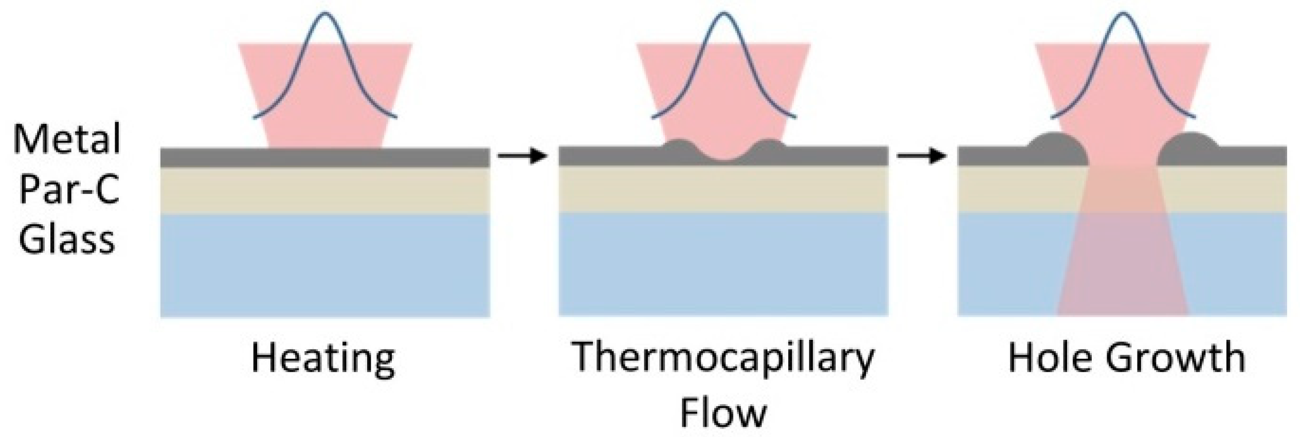
Figure 1. The mechanism for direct-write dewetting using a focused near-infrared (NIR) laser radiation.
Applsci 09 03165 g001
Figure 2. Optical micrographs (upper) and profilometry (lower) of Ni digits for pitch lengths of (a) 100 µm and (b) 40 µm. Optical micrographs have been aligned with the profiles for comparison. Yellow shading has been used to demark the polymer substrate in the profile; grey shading has been used to demark the native Ni-film layer.
Applsci 09 03165 g002
Figure 3. 3D profilometry mapping of a Ni linear array formed by directed dewetting with a spacing of 100 µm. “Negative” and “Positive” relate to the surface of the original Ni film. Of the accounted volume, an 11.5% excess positive volume remains unaccounted for after the dewetting process. This is attributed to shadowing effects from the measurement and the shape of the features.
Applsci 09 03165 g003
Figure 4. Cross-sectional FESEM images of Ni dewetted arrays for (a) 100 µm and (b) 40 µm pitched arrays. Ni is highlighted in red. The conductive epoxy used to pot the samples contained flakes of Ag, which appear above and around the film structures. The Par-C polymer substrate is the black area at the bottom of each image. The magnified areas are composed of the displaced dewetted Ni, which has cooled as beads along the laser pathway, which is perpendicular to the plane of the image.
Applsci 09 03165 g004
Figure 5. Optical microscopy of a dewetted Ag film on the Par-C polymer substrate. The laser scan of the dewetted Par-C surface appears along the dark center with ridges of dewetted metal along the edge. The beam was scanned in the direction of the arrow. Dewetted silver ridges exhibit an instability and degrade into discrete beads.
Applsci 09 03165 g005
Figure 6. 3D profilometry mapping of an Ag linear array formed by directed dewetting with a spacing of 100 µm. “Negative” and “Positive” relate to the surface of the original Ni film. The accounting of the displaced volume reveals that 7.9% of the excess positive space remains unaccounted for after the dewetting process.
Applsci 09 03165 g006
Figure 7. Red, color-enhanced, cross-sectional images of dewetted ridges of Ag for (a) 100 µm and (b) 40 µm pitched arrays. The right and left sides of two adjacent digits are shown.
Applsci 09 03165 g007
Figure 8. The color enhanced, dewetted ridge profiles of 100 µm pitched line arrays for a cross section of a single digit in (a) Bi-Ag and (b) Ni-Ag layered target films. A diagram of the (c) film structure has been provided for clarity. The flakes in the image are related to the Ag conductive epoxy used for the specimen preparation.
Applsci 09 03165 g008
Figure 9. EDS elemental maps created from multi-layered (a,b) Bi/Ag and (c,d) Ni/Ag films where Ag is the base film displayed as red and Bi or Ni is used as an absorption layer displayed as green. In (a,c), only the base film is shown in red, while (b,d) display the base film with the absorption film overlaid in green.
Applsci 09 03165 g009
Figure 10. Cross section EDS maps of the dewetted and displaced “ridge” portion of (ac) Bi-Ag layered films and (df) Ni-Ag layered films after the dewetting process described in the text. The EDS shows a contrast in the elemental distributions. A segregated displaced layer of Ni (f) is shown to encapsulate the displaced Ag shown in (e) during the dewetting process of the Ni/Ag films. This is in contrast to the mixed phase of Bi with Ag for the dewetted Bi/Ag films. The arrow indicates the dewetted and displaced metal “ridge”. The other Ag is from the conductive epoxy utilized for the specimen preparation.
Applsci 09 03165 g010
Figure 11. An inter-digit electrode composed of 45 pairs of digits with 30 μm spacing and an 80 μm width formed from a scanning laser dewetted Ag film deposited upon a Par-C polymer, imaged using (a) FESEM. The IDE can be removed from the glass slide as (b,c) a flexible and free-standing film.
Applsci 09 03165 g011
Figure 12. A color-enhanced example of a push structure using 640 nm nickel films on Par-C substrates, as characterized by (a) profilometry and (b) FESEM. Successive, overlapping laser scans induce a progressive and directional dewetting front in the nickel film that produces thicker, smoother ridges without the need for additional depositions. Yellow demarks the Par-C, while grey demarks the original surface of the nickel. The dotted square highlights the pushed ridge.
Applsci 09 03165 g012
Table 1. Physical attributes of various substrate or target film chemistries.
MaterialM.P.Surface Energy/Tension [mJ/m2]Inherent Absorptivity at 1064 nm [%]Thermal Conductivity [W/(m∙K)]Electrical Resistivity [Ω∙m]
SolidLiquid
Borosilicate Glass821 [29] (soften)253.0 [30]-< 3 [31]1.058 × 10⁸
Parylene-C290 [32]19.6 [32]-< 15 [33]0.0821 × 10¹⁵
Polyimide400 (soften)53-< 10 [34]0.151.5 × 1015
PTFE32720-< 10 [34]0.26 [35]1 × 10²³
Bi271.5 [35]446 [36]378 [36]32 17.87 [35]107 × 10−8 [35]
Sn231.93 [35]661 [36]560 [36]54 166.6 [35]11.5 × 10⁻⁸ [35]
Ni1455 [35]2080 [36]1763 [36]28 190.7 [35]6.93 × 10⁻⁸ [35]
Ag962 [35]1086 [36]920 [36]< 5 1429 [35]1.587 × 10⁻⁸ [35]
1 Calculated from optical constants.