Article

Bridgeless Buck-Boost PFC Rectifier with Positive Output Voltage

Department of Electrical Engineering, National Taipei University of Technology, 1, Sec. 3, Zhongxiao E. Rd., Taipei 10608, Taiwan
*
Author to whom correspondence should be addressed.
Appl. Sci. 2019, 9(17), 3483; https://doi.org/10.3390/app9173483
Submission received: 18 July 2019 / Revised: 20 August 2019 / Accepted: 20 August 2019 / Published: 23 August 2019
(This article belongs to the Section Electrical, Electronics and Communications Engineering)

Abstract

:
A bridgeless buck-boost power-factor-correction (PFC) rectifier with positive output voltage is proposed herein. This PFC rectifier operates in the discontinuous conduction mode (DCM). Owing to the DCM, a good performance on PF is easily achieved as well as no reverse recovery currents being generated from the diodes. By means of output voltage sensing along with the traditional voltage-follower control, a proper control force is created to drive the switches. By doing so, not only the output voltage is stably controlled at a given value, but also the input current tracks the input voltage as tightly as possible. In addition, the accompanying harmonic distortion meets the requirements of the IEC6100-3-2 Class C harmonics standard, and accordingly, the proposed rectifier is suitable for the AC-DC LED driver. Finally, via mathematical deductions and experimental results, the effectiveness of the proposed bridgeless buck-boost PFC rectifier is verified.

1. Introduction

The AC-DC rectifier with power factor correction (PFC) takes an important role not only in energy saving but also in reduction of the total harmonic distortion (THD). Harmonics standards, such as IEC61000-3-2 [1], JIS-C-61000-3-2, etc., are offered to limit the harmonics generated from the electronic products. For example, the electronic products with output power above 75 W need to pass the corresponding harmonics tests.
There are two kinds of PFC rectifiers. The first kind is named passive PFC rectifier [2,3], which is mainly built up by the inductor, the capacitor and the diode. This kind possesses advantages of circuit simplicity, low cost, and so on, but has disadvantages of large size, heavy weight, low efficiency, low circuit flexibility, and so on. Since the passive PFC rectifier does not work well, the second kind, named active PFC rectifier, is proposed [4,5]. Generally, this kind is mainly constructed by the switch, the inductor, and the diode. The rectifier can make the input current tightly track the input voltage via the proper turning-on of the switch under different input voltages and various output loads. By doing so, the input current can easily meet the required harmonics standard. Compared with the passive PFC rectifiers, the active PFC rectifier has many advantages, such as small size, light weight, high power density, high PF, low THD, etc.
There are three kinds of non-isolated converters widely utilized in the active rectifier: boost, buck, and buck-boost converters. Among them, the active PFC boost rectifier is commonly employed [6,7,8]. The key merit of this kind is that the current in the input inductor operates in the continuous conduction mode (CCM), thereby obtaining a high PF and a low THD. However, such a kind can be used only under the condition that the output voltage is larger than the peak value of the input voltage.
Consequently, the active buck PFC rectifier is presented [9,10,11]. Such a rectifier can transfer a high input AC voltage to a low DC voltage. However, as the input voltage is lower than the output voltage, there is no input current, thus making zero-crossing distortion occur. Consequently, even if this rectifier operates in the CCM, the PF is relatively low and the THD is relatively high.
Based on the aforementioned, the active buck-boost PFC rectifier is proposed [12,13,14]. In the CCM, such a PFC rectifier possesses relatively high variations in output voltage due to step-up/step-down of the input voltage. However, the output voltage of this rectifier is negative. Consequently, its industrial applications are limited.
On the other hand, the power loss in low-frequency diodes of the traditional active PFC rectifier is huge. Hence, to remove this diode loss, some researchers present bridgeless active PFC rectifiers using high-frequency diodes and switches [15,16,17].
Accordingly, a bridgeless buck-boost PFC rectifier with positive output voltage is proposed herein. This circuit is derived from the circuit shown in [17] by Jovanovic, M.M.; Jang, Y. The total component count of the proposed circuit is the same as that of the circuit shown in [17]. Basically, there is a difference in specifications between the proposed circuit and the circuit shown in [17], and the comparison between the two is not easy. However, from the point of view of voltage gain in the BCM or CCM, the former has a value of D/(1-D), locating between zero and infinity, where D is the duty cycle, and the latter has a value of 2D, locating between zero and two. This means that the former has relatively low zero crossover distortion as compared to the latter. Namely, the proposed circuit has better performance of PFC and THD than the circuit shown in [17] has. Furthermore, in the proposed circuit, the rectification switches S1 and S2 are back-to-back cascaded in the opposite direction, and thus only one gate driver is required.

2. Overall System Configuration

Figure 1 displays the overall system configuration for the proposed circuit. The main power stage contains four high-switching-frequency diodes, D1, D2, D3, and D4, three high-switching-frequency switches, S1, S2 and S3 with individual gate drivers, one output diode Do, one output capacitor Co, and one inductor L. Regarding the control stage, it contains one voltage divider, one analogue-to-digital converter, named ADC, and one field programmable gate array, named FPGA. The output resistor is signified by R. Note that the switch S3 is utilized to make the output voltage positive.
The output voltage is sensed from the main power stage and passed to the voltage divider and then to the ADC to generate a digital value. Afterwards, such a digital value is passed to the controller embedded in the FPGA to yield three proper PWM signals for S1, S2 and S3. Note that the voltage-follower control is employed herein. This is because if the main power stage operates in the DCM, the corresponding power factor is inherently high [18].
In addition, the proportional-integral (PI) controller embedded in the FPGA can make the proposed converter operated stably. The parameters of this controller are obtained by the industrial try-and-error tuning method as follows.
Step 1
Under the input nominal voltage of 110 Vrms and rated output power, the integral gain ki is first set to zero, and then the proportional gain kp is gradually increased, so that the value of kp stops being increased until the output voltage reaches 75% of the desired value.
Step 2
Under the same conditions, the value of kp obtained from step 1 is fixed, and then the value of ki is gradually increased, so that the output voltage is stabilized at the desired value without oscillation.
Step 3
Under the input nominal voltage of 110 Vrms but different output powers, the values of kp and ki are finely tuned, so that the output voltage is stabilized at the desired value for all the output power range.
Step 4
Change the input voltage levels, and repeat step 3, so that the output voltage is stabilized at the desired value for all the input voltage range and all the output power range.

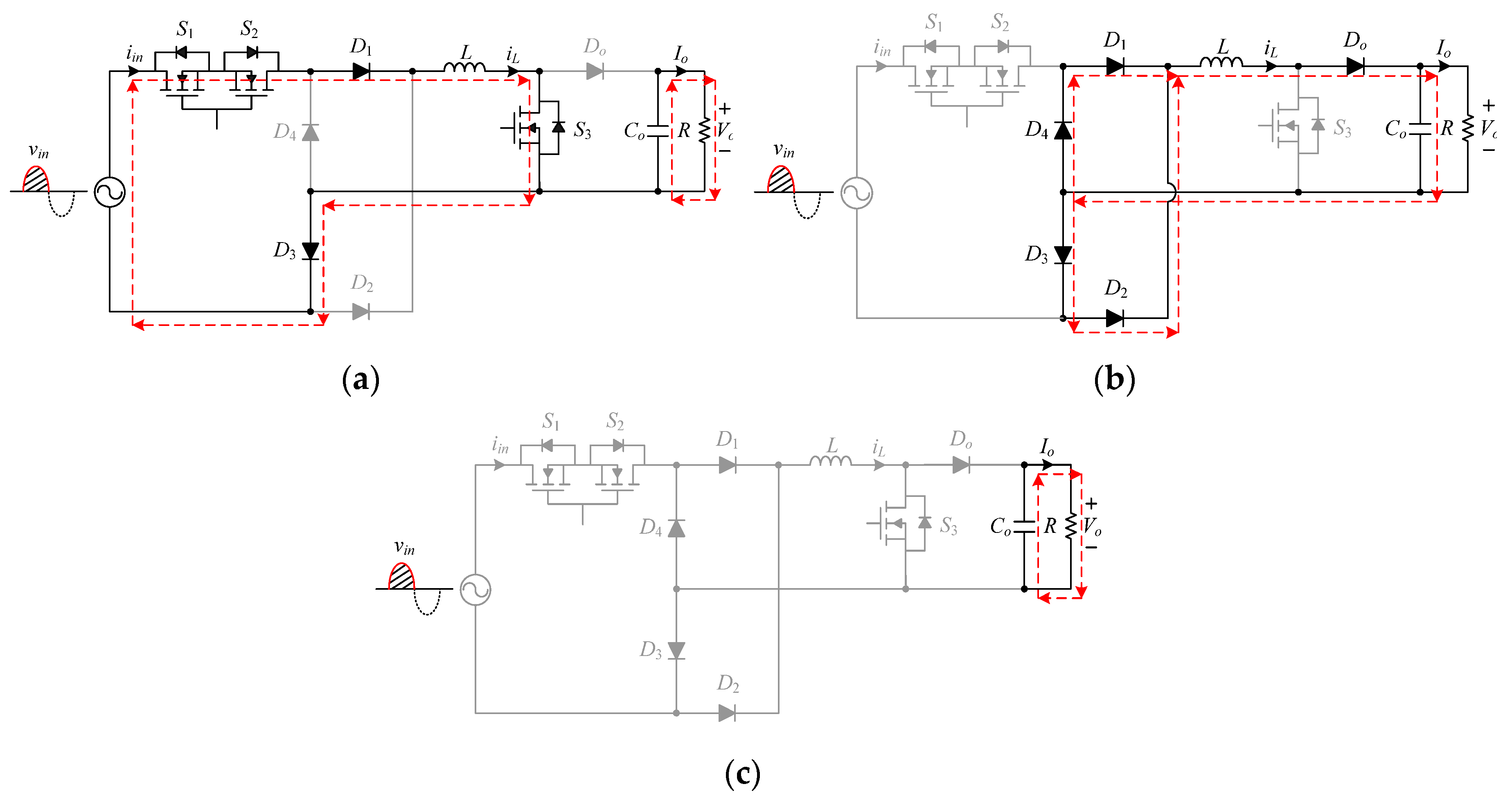
3. Basic Operating Principles

For analysis convenience, some assumptions are given below:
(1).
All the switches, diodes, inductor and capacitor are considered as ideal.
(2).
The PWM signals for S1, S2 and S3 are the same.
(3).
The value of Co is large enough to render the voltage across it constant at Vo.
(4).
The circuit operates in the DCM.
According to these above assumptions, Figure 2 shows the key waveforms for the proposed PFC rectifier operating under the positive input voltage. There are six states are to be described as following.
(1)
State 1 [ 0 t D T s ]: As the voltage vin is positive, S1, S2, S3, D1, and D3 are ON, whereas D2, D4, and Do are OFF. During this state, the current iin flows through S1, S2, S3, D1, D3, and L, as shown in Figure 3a. At the same time, as shown in Figure 2, the voltage across L is vin, making L magnetized and the current iL increasing linearly. Moreover, the output energy needed is offered by Co.
(2)
State 2 [ D T s t ( D + Δ ) T s ]: As the input voltage is still positive, S1, S2, and S3 are OFF, whereas D1, D2, D3, D4 and Do are ON. During this state, the current iin is zero, whereas the current iL continuously flows through these five diodes, as shown in Figure 3b. At the same time, as shown in Figure 2, the voltage across L is V o , rendering L is demagnetized and the current iL decreasing linearly. In addition, the output energy needed is provided by the energy stored in L.
(3)
State 3 [ ( D + Δ ) T s t T s ]: As the input voltage still keeps positive, S1, S2, S3, D1, D2, D3, D4 and Do are OFF, as shown in Figure 3c. Namely, there is no current flowing through L, as shown in Figure 2, and hence the output energy needed is supplied from Co.
For the negative input voltage to be considered, there are also three states, that is, states 4, 5 and 6. The behavior in state 4 is similar to that in state 1 except that the diodes D1 and D3 conducted in state 1 is replaced by the diodes D2 and D4 conducted in state 4. Also, the behaviors in states 5 and 6 are the same as those in states 2 and 3, respectively.
Based on the volt-second balance for the inductor L, the following equation must be held:
1 L · v i n · D · T s + 1 L · ( V o ) · Δ 1 · T s + 1 L · 0 · Δ 2 · T s = 0
Also,
D + Δ 1 + Δ 2 = 1
By rearranging (1) according to (2), the voltage gain can be obtained:
V o v i n = D Δ 1
Equation (3) is only for the convertor working in the DCM. But if the converter operates in the BCM or CCM, then the value of Δ 2 will be zero and the voltage gain shown in (3) can be rewritten to
V o v i n = D 1 D

4. Design Considerations

Before we tackle this section, some specifications and assumptions are given below: (i) the input voltage range locates between 90 Vrms and 130 Vrms with a nominal voltage of 110 Vrms; (ii) the output voltage is set at 80 V; (iii) the output power range locates between 22.5 W and 90 W with a rated power of 90 W; (iv) the switching frequency is set at 100 kHz; (v) the rated-load efficiency under the minimum input voltage is set at assumed to be 90%; (vi) the line frequency is set at 60 Hz; (vii) the peak-to-peak value of the output voltage ripple is set at 3% of the output voltage; and (viii) the circuit always works in the DCM except that the circuit works in the BCM at the peak input current which happens under the minimum input voltage and the rated output power.
Furthermore, the sampling frequency is 100 kHz, synchronous with the switching frequency. The number of sampling bits out of the ADC is 10 bits. The voltage ratio of the voltage divider is 3 over 80. The number of PWM signal bits out of the FPGA is 10 bits.
In addition, the product name for the switches S1 and S2 and is IXTQ88N28T. The product name for the switch S3 is STP120NF10. The product name for the diodes D1, D2, D3, and D4 is APT30D30BCT. The product name for the diode Do is MBR40100PT. The inductor L has a value of 58.5 μH based on a CM270125 core with 18 turns. The capacitor is constructed by two paralleled Nippon Chemi-Con capacitors, 650 μF//650 μF.

4.1. Inductor Design

Firstly, it is assumed that the voltage v i n and the current i i n are purely sinusoidal and in phase. Therefore,
v i n = V i n , p k sin θ
i i n = I i n , p k sin θ
where V i n , p k denotes the peak value of v i n , I i n , p k indicates the peak value of i i n , ω L equals 2 π f L , fL signifies the line frequency inversely proportional to the line period TL, and θ equals ω L t .
Therefore, the average input power P i n can be obtained:
P i n = 1 T L · t 0 t 0 + T L p i n ( θ ) d θ = 1 π · 0 π v i n · i i n d θ
By substituting (5) and (6) into (7), Pin can be rewritten as
P i n = 1 π · 0 π V i n , p k sin θ · I i n , p k sin θ d θ = V i n , p k I i n , p k π · 0 π sin 2 θ d θ = V i n , p k I i n , p k π · 0 π ( 1 cos 2 θ ) 2 d θ = V i n , p k I i n , p k 2
Secondly, it has been assumed that the circuit works in the BCM at the peak input current under the minimum input voltage Vin,min,pk, named Iin,pk,max, and the rated output power Po,rated. By taking the rated-load efficiency under the minimum input voltage, named η , into consideration, Iin,pk,max can be represented based on (8) as
I i n , p k , m a x = 2 · P o , r a t e d / η V i n , m i n , p k
By putting the numerical values into (9), the calculated value of Iin,pk,max can be obtained:
I i n , p k , m a x = 2 × 90 / 0.9 90 2 = 1.57 A
Thirdly, since the circuit works in the BCM only at the peak input current under the minimum input voltage and the rated output power, the maximum value of the peak value of iL, named I L , p k , m a x , can be represented by
I L , p k , m a x = I i n , p k , m a x D
where D corresponds to the peak value of iL under the minimum input voltage and the rated output power.
Fourthly, the peak-to-peak value of iL, named Δ i L , can be expressed as
Δ i L = V o ( 1 D ) T s L
Hence, if the inductor L operates in the DCM, the following criterion must be held:
I L , a v g , p k Δ i L 2 I i n , p k , m a x D V o ( 1 D ) T s 2 L L V o D ( 1 D ) T s 2 I i n , p k , m a x
Eventually, according to (10) and the specifications expressed at the beginning of Section 4, the following criterion based on (13) can be obtained:
L 80 × 0.386 × ( 1 0.386 ) × 10 μ 2 × 1.57 = 60.38 μ H
Hence, the value of L is set at 58.5 μH.

4.2. Output Capacitor Design

According to (5) and (6), the instantaneous input power p i n ( t ) can be represented by
p i n ( t ) = V i n , p k sin ω L t · I i n , p k sin ω L t = V i n , p k · I i n , p k ( 1 cos 2 ω L t ) 2
Also, the instantaneous output power po(t) can be written as
p o ( t ) = V o · i D o ( t )
By equalizing (15) and (16), the current flowing through Do, named iDo, can be expressed by
i D o ( t ) = V i n , p k · I i n , p k · η 2 V o · ( 1 cos 2 ω L t )
Based on (17), the current flowing through Co, named ic, can be obtained to be
i c ( t ) = V i n , r m s · I i n , r m s · η V o · ( cos 2 ω L t ) = I o cos 2 ω L t
where Io is the output current.
Also,
v c ( t ) = 1 C o i c ( t ) d t
Therefore, based on (18) and (19), the output voltage ripple v ˜ o can be represented as
v ˜ o ( t ) = I o 2 ω L C o sin 2 ω L t
From (20), the peak-to-peak value of the output voltage ripple, named Δvo, can be expressed as
Δ v o = I o ω L C o
Since the value of Δvo is set at 3% of Vo, the value of Δvo can be obtained:
Δ v o = V o · 3 % = 80 × 0.03 = 2.4 V
According to (21), (22) and the specifications given at the beginning of Section 4, the value of Co can be worked out by setting Io at the rated output current:
C o = I o ω L Δ v o = 1.125 2 π × 60 × 2.4 = 1243.4 μ F
Eventually, two Nippon Chemi-Con 650 μF capacitors, connected in parallel, are selected as Co.

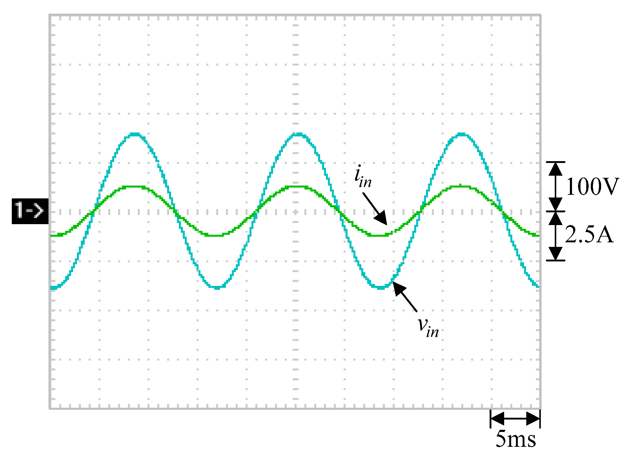
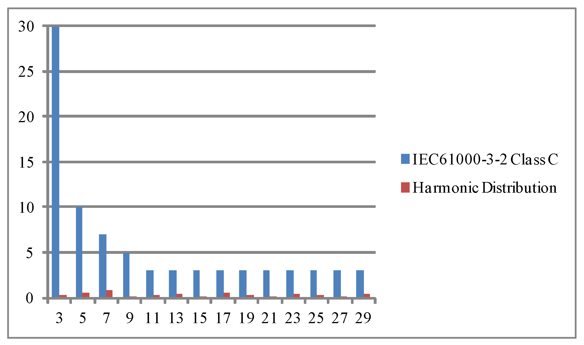
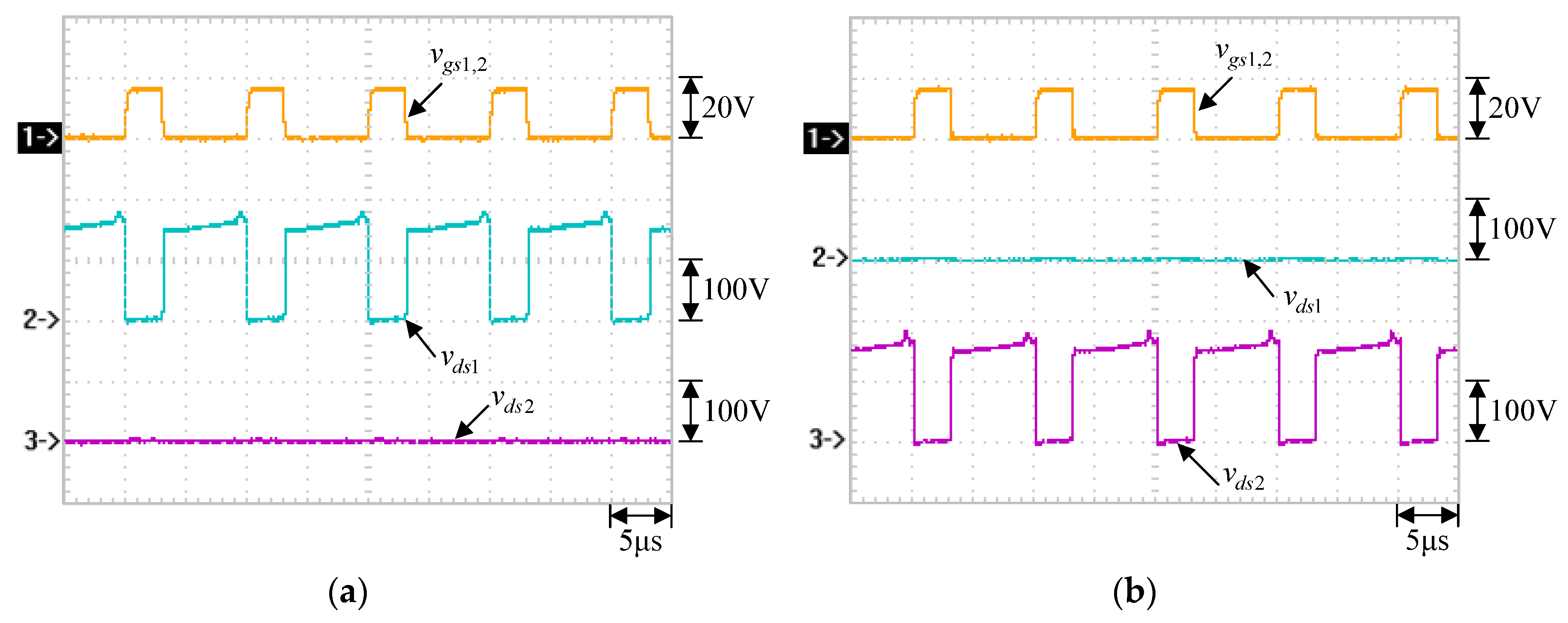
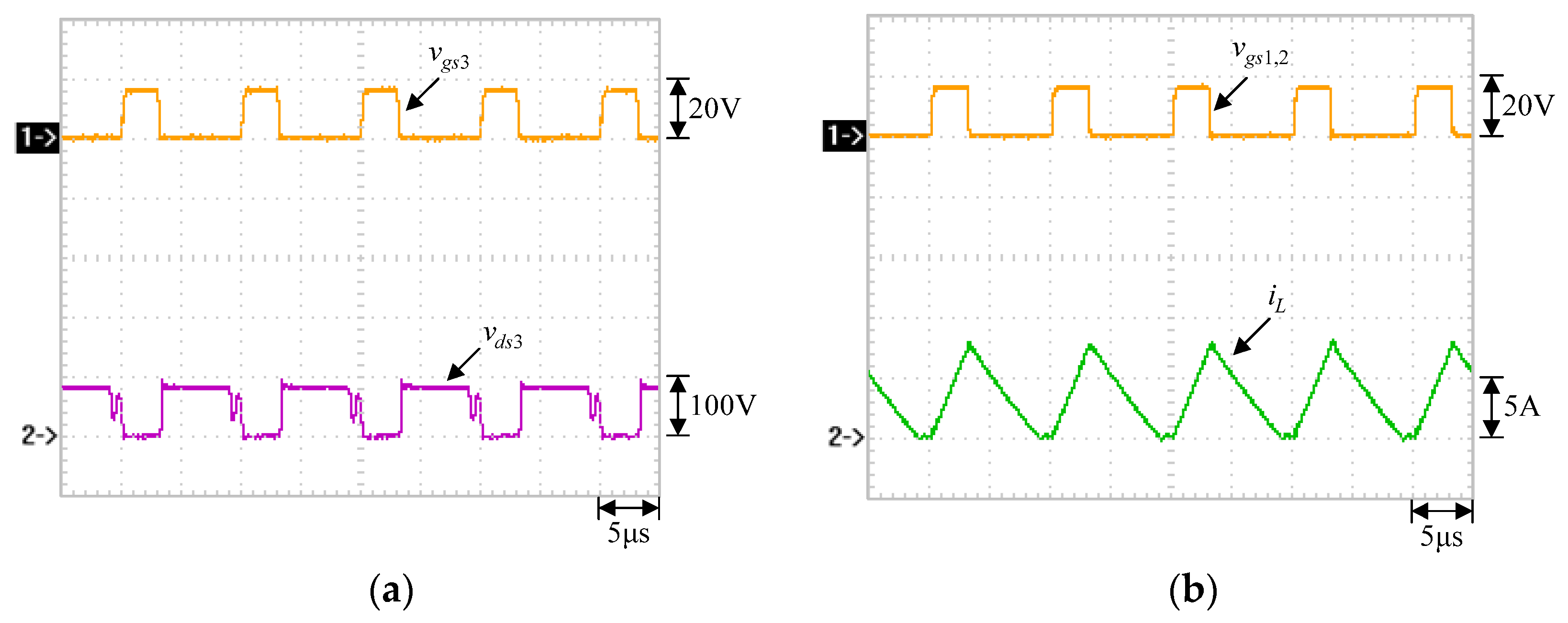
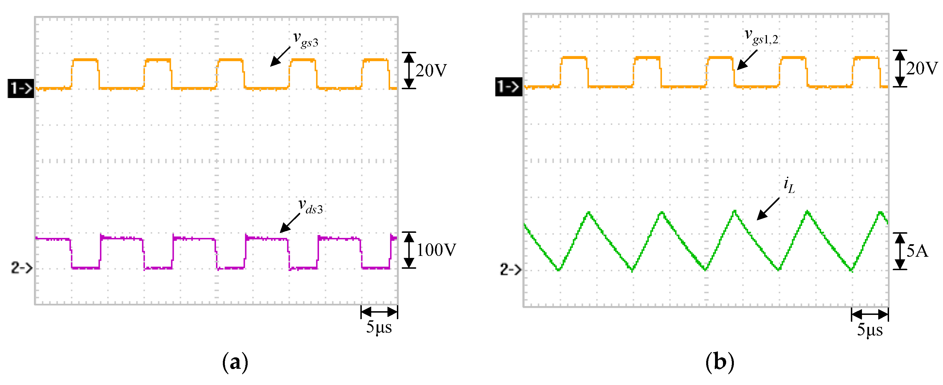
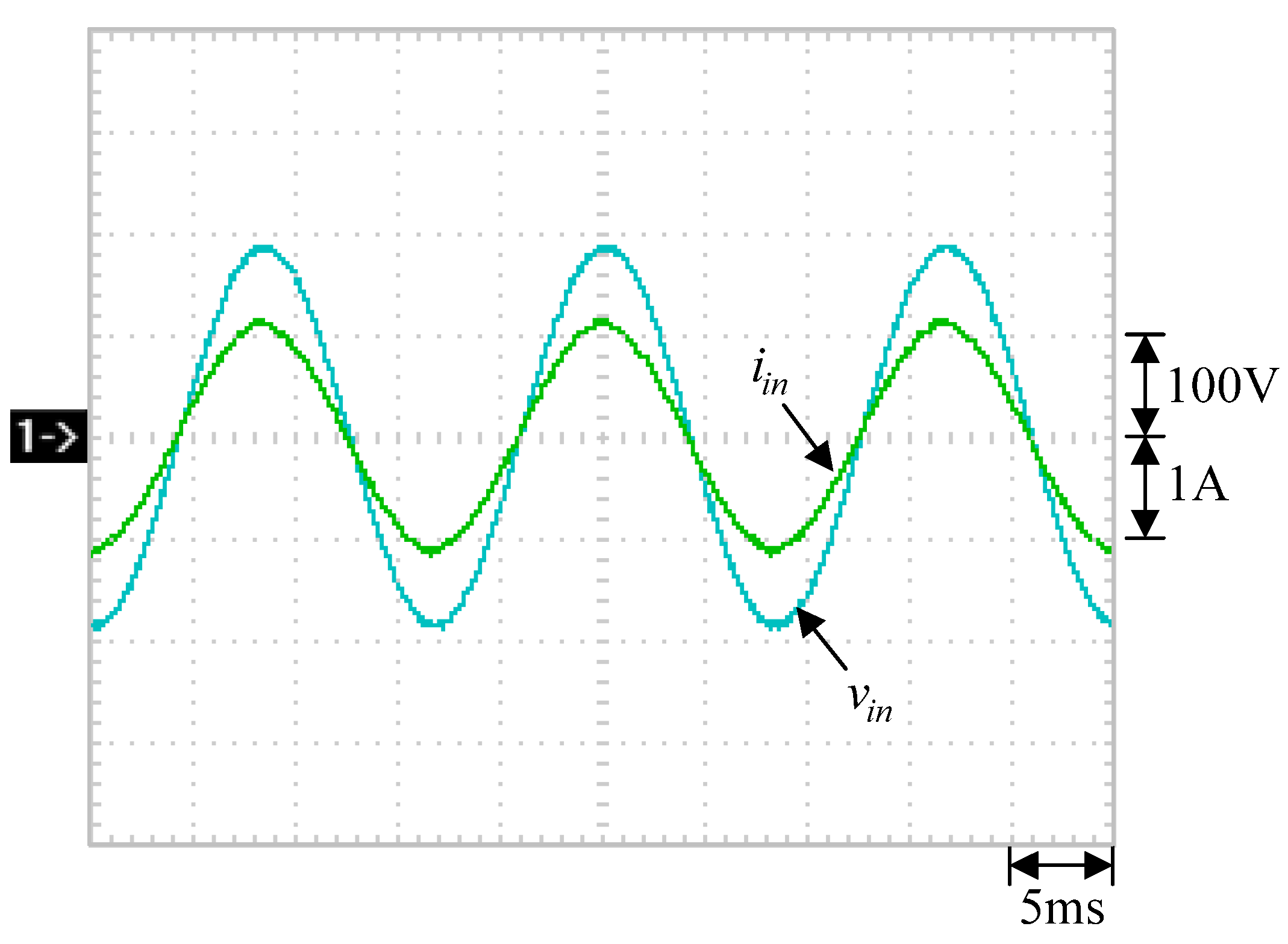
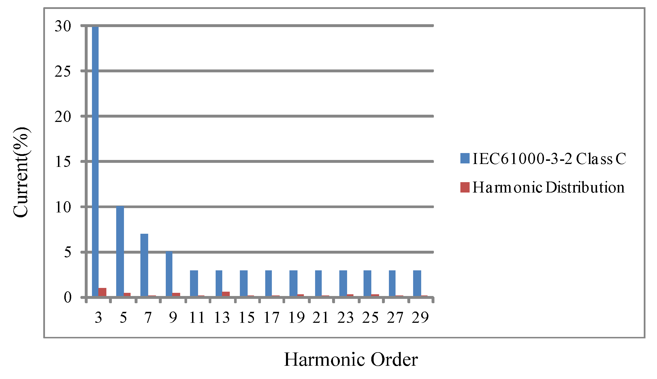
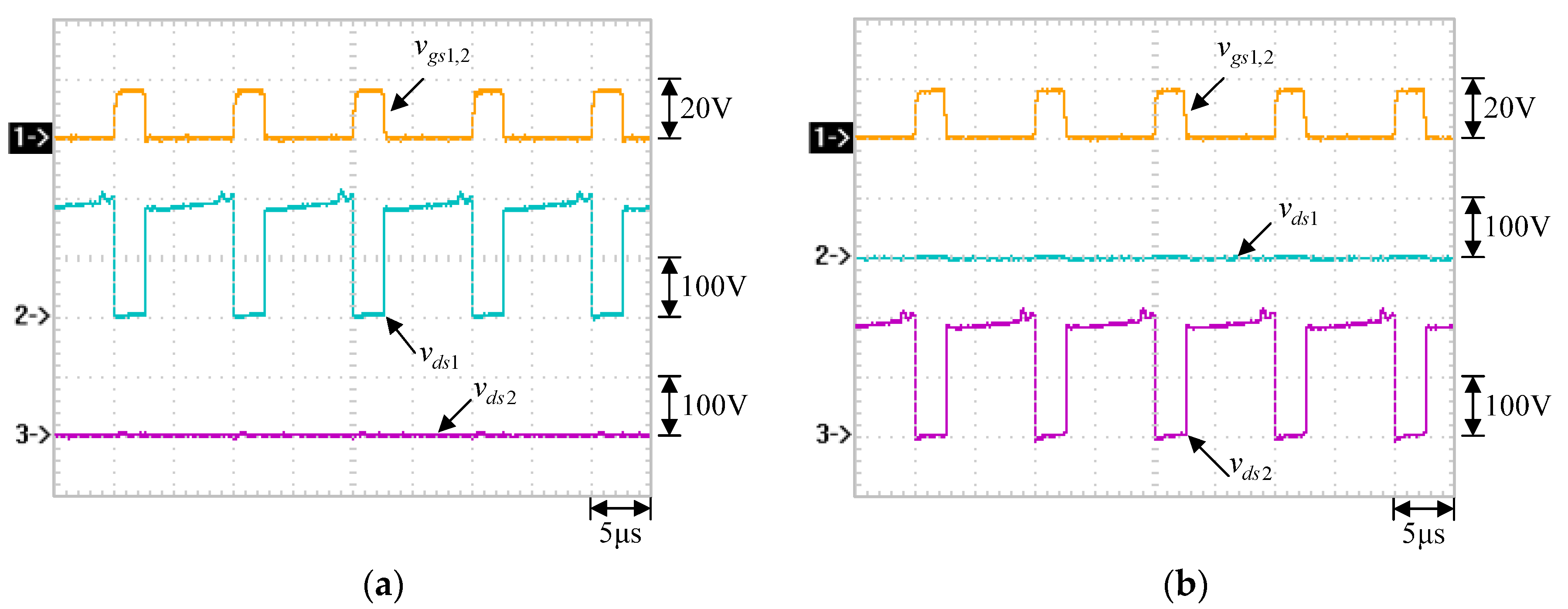
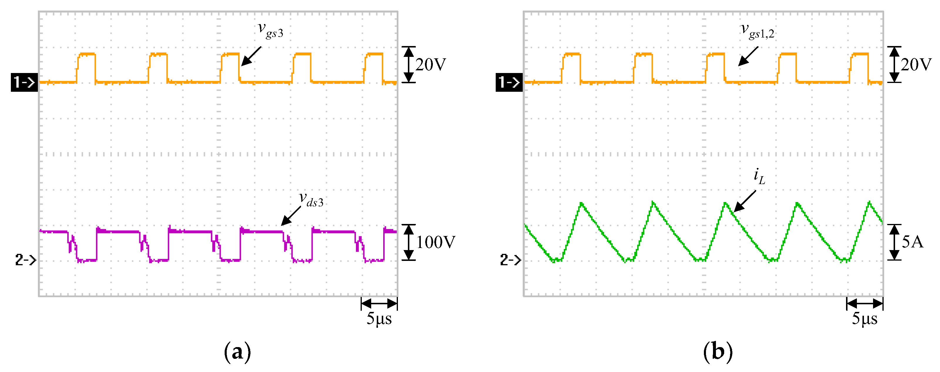
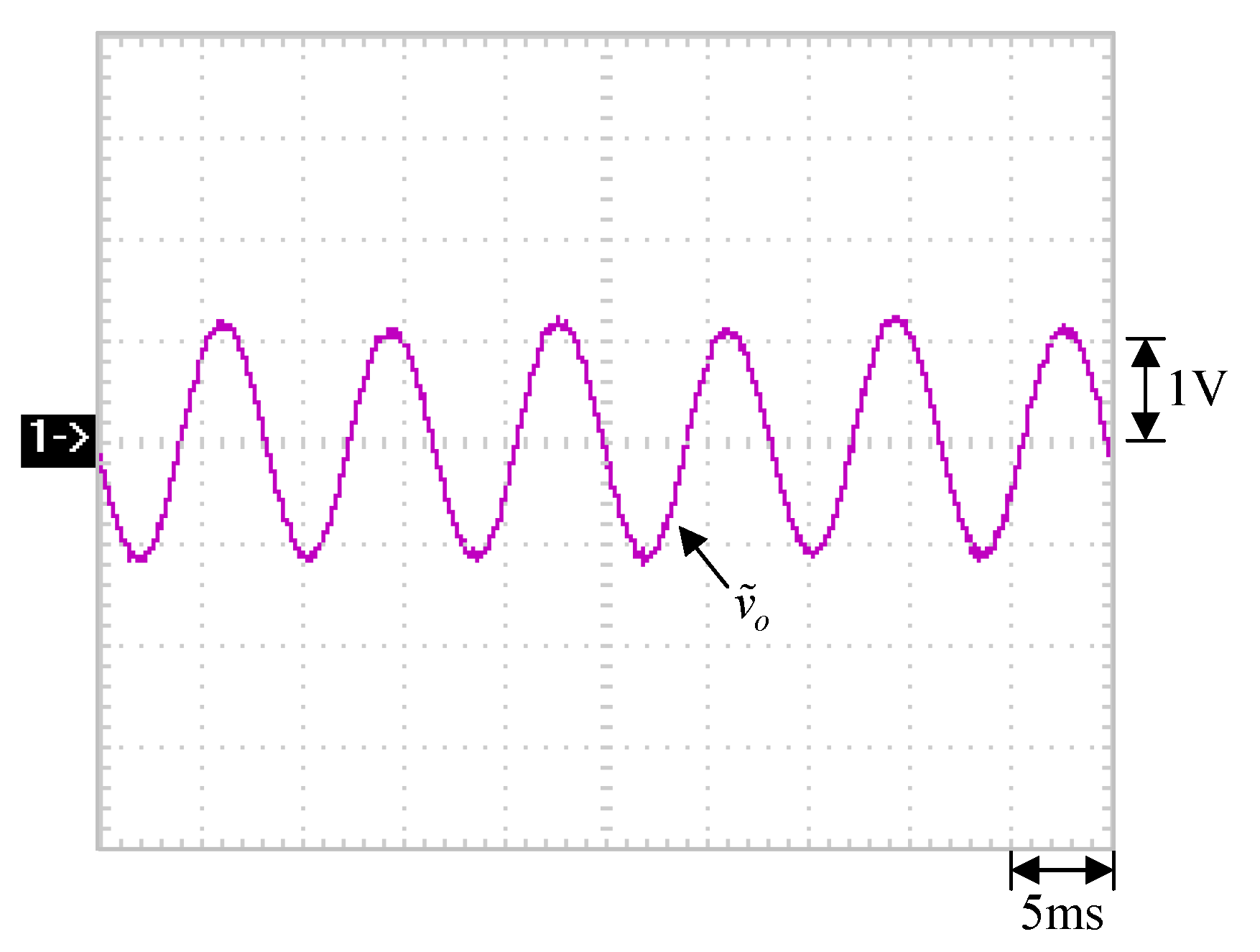
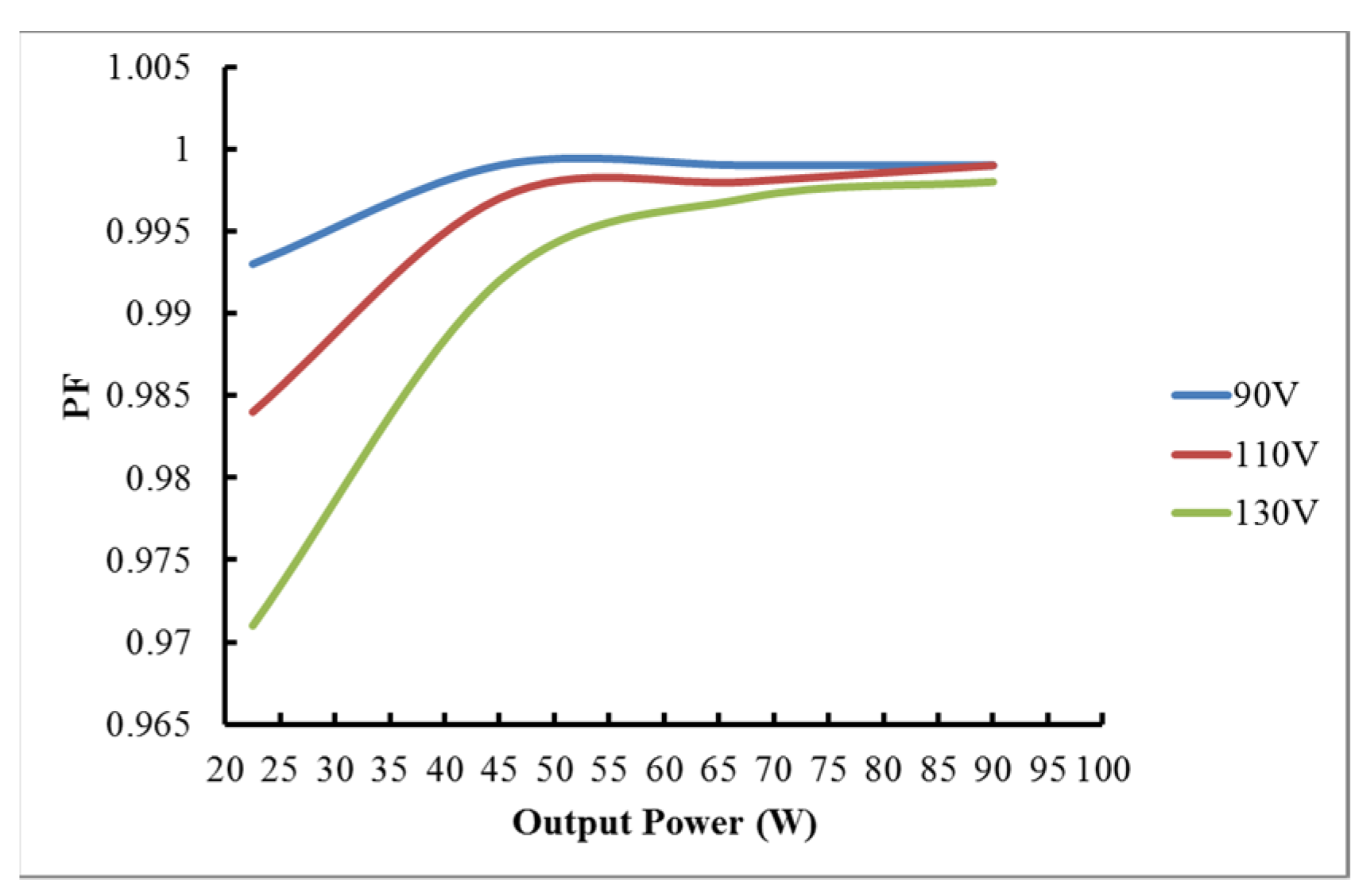
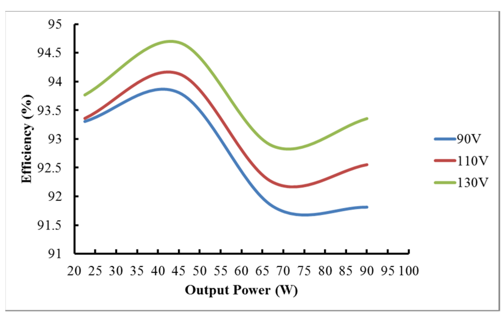
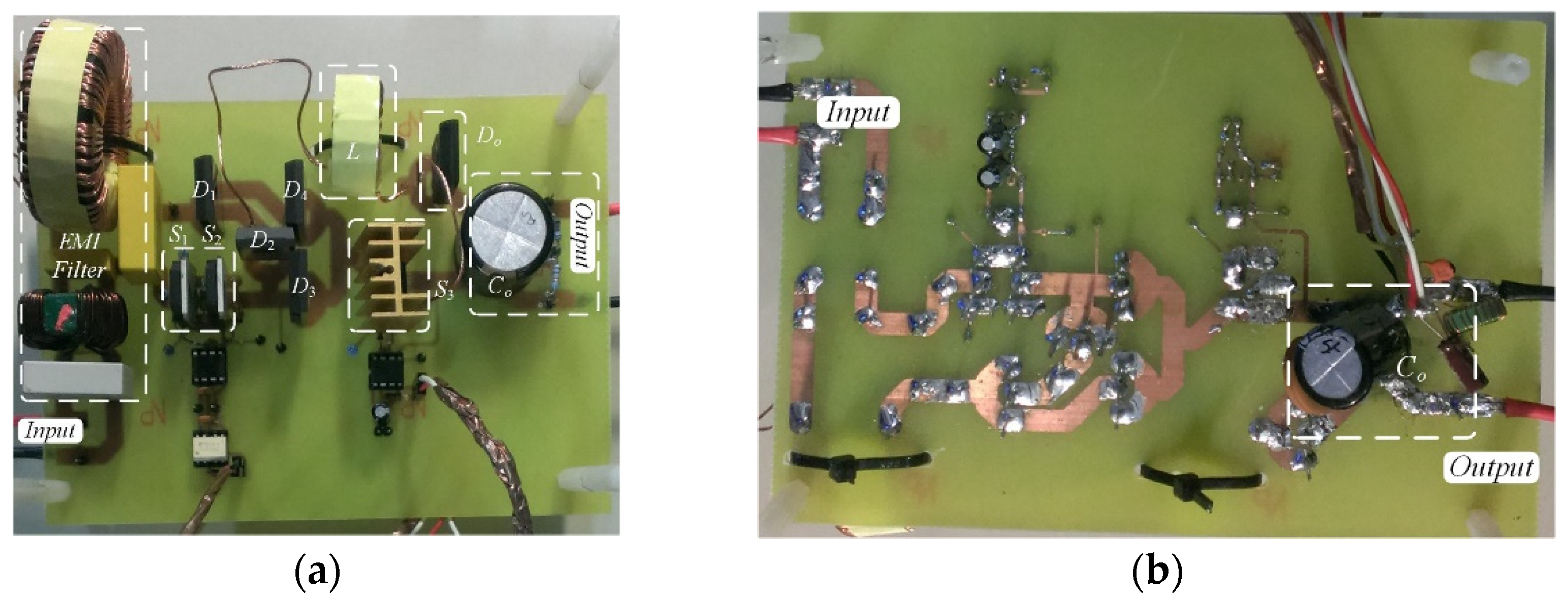
5. Experimental Results

Prior to this section, an input filter with corner frequency of about 10 kHz, constructed by one inductor of 500 μH and one capacitor of 470 nF, is put between the input voltage and the circuit, so as to remove high-frequency component of the input current. Figure 4, Figure 5, Figure 6, Figure 7 and Figure 8 are measured at the rated output power and the input voltage of 110 Vrms. Figure 4 displays the input voltage vin and the input current iin. From Figure 4, it can be seen that the input current iin tracks the input voltage vin as tightly as possible, so as to realize power factor correction. Figure 5 shows the input current harmonic distribution, which meets IEC61000-3-2 Class C. Under the positive input voltage, Figure 6a displays the PWM signal for both S1 and S2, named vgs1,2, and the voltages across the switches S1 and S2, named vds1 and vds2, whereas under the negative input voltage, Figure 6b shows the PWM signal for both S1 and S2, named vgs1,2, and the voltages across the switches S1 and S2, named vds1 and vds2. From Figure 6a,b, as the switch S1 or S2 is turned off, the voltage across S1 or S2 is about 180 V. Note that under the positive cycle, as the PWM signal is low, the voltage across S1 is high but the voltage across S2 is zero due to forward bias of the body diode of S2, whereas under the negative cycle, as the PWM signal is low, the voltage across S2 is high but voltage across S1 is zero due to forward bias of the body diode of S1. Figure 7a displays the PWM signal vgs3, and the voltage across the switch S3. From Figure 7a, as the switch S3 is turned off, the voltage across S3 is about 80 V. Figure 7b shows the PWM signal for both S1 and S2, named vgs1,2, and the current in L1, named iL, whereas Figure 8 displays the low-frequency output voltage ripple v ˜ o . From Figure 7b, it can be seen that the inductor works in the DCM, whereas from Figure 8, it can be seen that the peak-to-peak value of v ˜ o is about 2.4 V, close to (22).
In addition, by the same way, Figure 9, Figure 10, Figure 11, Figure 12 and Figure 13 are measured under the input voltage of 90 Vrms, whereas Figure 14, Figure 15, Figure 16, Figure 17 and Figure 18 are measured under the input voltage of 130 Vrms.
Figure 19 displays the curves of total harmonic distortion versus output power under three input voltage levels. From this figure, it can be seen that all the values of THD are within 2%. Figure 20 shows the curves of power factor versus output power under three input voltage levels. From this figure, it can be seen that all values of PFC are above 0.971. Figure 21 displays the curves of efficiency versus output power under three input voltage levels. From this figure, it can be seen that all the efficiency is above 91% and the efficiency can be up to 94.68%. In addition, Figure 22 shows a photo of the proposed circuit.

6. Conclusions

A bridgeless buck-boost PFC rectifier with positive output voltage is proposed herein. For implementation convenience, this rectifier is operated in the DCM based on the voltage-mode control. By doing so, this rectifier has good performance on THD and PF, along with the output voltage controlled at a desired value. Moreover, the harmonic distortion meets the requirements of the IEC6100-3-2 Class C harmonics standard, and hence the proposed circuit is suitable for the AC-DC LED driver.

Author Contributions

The conception was presented by K.-I.H., who also was responsible for editing this paper. Y.-K.T. surveyed the existing papers and wrote the software program. Y.-P.H. carried out experimental setup and verification. K.-I.H. was in charge of project administration.

Funding

This research was funded by the Ministry of Science and Technology, Taiwan, under the Grant Number: MOST 107-2221-E-027-023.

Acknowledgments

The authors gratefully acknowledge the support of the Ministry of Science and Technology, Taiwan, under the Grant Number MOST 107-2221-E-027-023.

Conflicts of Interest

The authors declare no conflict of interest with commerce.

References

  1. IEC61000-3-2. Electromagnetic Compatibility (EMC)-Part3-2: Limits–Limits for Harmonic Current Emissions (Equipment Input Current ≤ 16 A Per Phase); International Electrotechnical Commission (IEC): Geneva, Switzerland, 2005. [Google Scholar]
  2. Prasad, A.R.; Ziogas, P.D.; Mania, S. A novel passive waveshaping method for single-phase diode rectifiers. IEEE Trans. Ind. Electron. 1990, 37, 521–530. [Google Scholar] [CrossRef]
  3. Seidel, A.R.; Bisogno, F.E.; Pappis, D.; Dalla Costa, M.A.; do Prado, R.N. Simple valley-fill self-oscillating electronic ballast with low crest factor using pulse-frequency modulation. In Proceedings of the 38th IAS Annual Meeting on Conference Record of the Industry Applications Conference, Salt Lake City, UT, USA, 12–16 October 2003; pp. 779–784. [Google Scholar]
  4. Umesh, S.; Venkatesha, L.; Usha, A. Active power factor correction technique for single phase full bridge rectifier. In Proceedings of the 2014 International Conference on Advances in Energy Conversion Technologies (ICAECT), Anipal, India, 23–25 January 2014; pp. 130–135. [Google Scholar]
  5. Wu, H.; Ge, H.; Xu, Y.; Zhang, W. The power factor correction of three-phase to single-phase matrix converter with an active power decoupling capacity. In Proceedings of the 2014 International Conference on Advances in Energy Conversion Technologies (ICAECT), Manipal, India, 23–25 January 2014; pp. 1–5. [Google Scholar]
  6. Zhang, J.; Shao, J.; Xu, P.; Lee, F.C.; Jovanovic, M.M. Evaluation of input current in the critical mode boost PFC converter for distributed power systems. In Proceedings of the APEC 2001 Sixteenth Annual IEEE Applied Power Electronics Conference and Exposition (Cat. No.01CH37181), Anaheim, CA, USA, 4–8 March 2001; Volume 1, pp. 130–136. [Google Scholar]
  7. Das, P.; Pahlevaninezhad, M.; Drobnik, J.; Moschopoulos, G.; Jain, P.K. A nonlinear controller based on a discrete energy function for an AC/DC boost PFC converter. IEEE Trans. Power Electron. 2013, 28, 5458–5476. [Google Scholar] [CrossRef]
  8. Pahlevani, M.; Pan, S.; Eren, S.; Bakhshai, A.; Jain, P. An adaptive nonlinear current observer for boost PFC AC/DC converters. IEEE Trans. Ind. Electron. 2014, 61, 6720–6729. [Google Scholar] [CrossRef]
  9. Vahedi, H.; Al-Haddad, K. A novel multilevel multioutput bidirectional active buck PFC rectifier. IEEE Trans. Ind. Electron. 2016, 63, 5442–5450. [Google Scholar] [CrossRef]
  10. Keogh, B.; Young, G.; Wegner, H.; Gillmor, C. Design considerations for high efficiency buck PFC with half-bridge regulation stage. In Proceedings of the 2010 Twenty-Fifth Annual IEEE Applied Power Electronics Conference and Exposition (APEC), Palm Springs, CA, USA, 21–25 February 2010; pp. 1384–1391. [Google Scholar]
  11. Wu, X.; Yang, J.; Zhang, J.; Xu, M. Design considerations of soft-switched buck PFC converter with constant on-time (COT) control. IEEE Trans. Power Electron. 2011, 26, 3144–3152. [Google Scholar] [CrossRef]
  12. Nishida, Y.; Motegi, S.; Maeda, A. A single-phase buck-boost AC-to-DC converter with high-quality input and output waveforms. In Proceedings of the 1995 IEEE International Symposium on Industrial Electronics, Dubrovnik, Croatia, 10–14 January 1995; Volume 1, pp. 433–438. [Google Scholar]
  13. Morizane, T.; Shimomori, W.; Taniguchi, K.; Kimura, N.; Ogawa, M. PWM technique for non-isolated three-phase soft-switching buck-boost PFC converter. In Proceedings of the 2007 Power Conversion Conference, Nagoya, Japan, 2–5 April 2007; pp. 1280–1285. [Google Scholar]
  14. He, M.; Zhang, F.; Xu, J.; Yang, P.; Yan, T. High-efficiency two-switch tri-state buck-boost power factor correction converter with fast dynamic response and low-inductor current ripple. IET Power Electron. 2013, 6, 1544–1554. [Google Scholar] [CrossRef]
  15. Tsai, H.-Y.; Hsia, T.-H.; Chen, D. A family of zero-voltage-transition bridgeless power-factor-correction circuits with a zero-current-switching auxiliary switch. IEEE Trans. Ind. Electron. 2011, 58, 1848–1855. [Google Scholar] [CrossRef]
  16. Mahdavi, M.; Farzanehfard, H. Bridgeless SEPIC PFC rectifier with reduced components and conduction losses. IEEE Trans. Ind. Electron. 2011, 58, 4153–4160. [Google Scholar] [CrossRef]
  17. Jovanovic, M.M.; Jang, Y. Bridgeless high-power-factor buck converter. IEEE Trans. Power Electron. 2011, 26, 602–611. [Google Scholar]
  18. Sebastian, J.; Cobos, J.A.; Lopera, J.M.; Uceda, J. The determination of the boundaries between continuous and discontinuous conduction modes in PWM DC-to-DC converters used as power factor preregulators. IEEE Trans. Power Electron. 1995, 10, 574–582. [Google Scholar] [CrossRef]
Figure 1. Overall system configuration for the proposed circuit.
Applsci 09 03483 g001
Figure 2. Voltage and current of the inductor operating in the discontinuous conduction mode (DCM) under the positive input voltage.
Applsci 09 03483 g002
Figure 3. Power flow in: (a) state 1; (b) state 2; (c) state 3.
Applsci 09 03483 g003
Figure 4. Experimental waveforms at rated output power under 110 Vrms input voltage: (1) vin; (2) iin.
Applsci 09 03483 g004
Figure 5. Experimental harmonics distribution at rated output power under 110 Vrms input voltage.
Applsci 09 03483 g005
Figure 6. Experimental waveforms at rated output power under: (a) the peak value of the positive cycle of 110 Vrms input voltage: (1) vgs1,2; (2) vds1; (3) vds2; (b) the valley value of the negative cycle of 110 Vrms input voltage: (1) vgs1,2; (2) vds1; (3) vds2.
Applsci 09 03483 g006
Figure 7. Experimental waveforms at rated output power under 110 Vrms input voltage: (a) (1) vgs3; (2) vds3; (b) (1) vgs1,2; (2) iL.
Applsci 09 03483 g007
Figure 8. Experimental output voltage ripple v ˜ o at rated output power under 110 Vrms input voltage.
Applsci 09 03483 g008
Figure 9. Experimental waveforms at rated output power under 90 Vrms input voltage: (1) vin; (2) iin.
Applsci 09 03483 g009
Figure 10. Experimental harmonics distribution at rated output power under 90 Vrms input voltage.
Applsci 09 03483 g010
Figure 11. Experimental waveforms at rated output power under: (a) the peak value of the positive cycle of 90 Vrms input voltage: (1) vgs1,2; (2) vds1; (3) vds2; (b) the valley value of the negative cycle of 90 Vrms input voltage: (1) vgs1,2; (2) vds1; (3) vds2.
Applsci 09 03483 g011
Figure 12. Experimental waveforms at rated output power under 90 Vrms input voltage: (a) (1) vgs3; (2) vds3; (b) (1) vgs1,2; (2) iL.
Applsci 09 03483 g012
Figure 13. Experimental output voltage ripple v ˜ o at rated output power under 90 Vrms input voltage.
Applsci 09 03483 g013
Figure 14. Experimental waveforms at rated output power under 130 Vrms input voltage: (1) vin; (2) iin.
Applsci 09 03483 g014
Figure 15. Experimental harmonics distribution at rated output power under 130 Vrms input voltage.
Applsci 09 03483 g015
Figure 16. Experimental waveforms at rated output power under: (a) the peak value of the positive cycle of 130 Vrms input voltage: (1) vgs1,2; (2) vds1; (3) vds2; (b) the valley value of the negative cycle of 130 Vrms input voltage: (1) vgs1,2; (2) vds1; (3) vds2.
Applsci 09 03483 g016
Figure 17. Experimental waveforms at rated output power under 130 Vrms input voltage: (a) (1) vgs3; (2) vds3; (b) (1) vgs1,2; (2) iL.
Applsci 09 03483 g017
Figure 18. Experimental output voltage ripple v ˜ o at rated output power under 130 Vrms input voltage.
Applsci 09 03483 g018
Figure 19. Curves of total harmonic distortion versus output power.
Applsci 09 03483 g019
Figure 20. Curves of power factor versus output power.
Applsci 09 03483 g020
Figure 21. Curves of efficiency versus output power.
Applsci 09 03483 g021
Figure 22. Photo of the prototype of the proposed circuit: (a) top view; (b) bottom view.
Applsci 09 03483 g022

