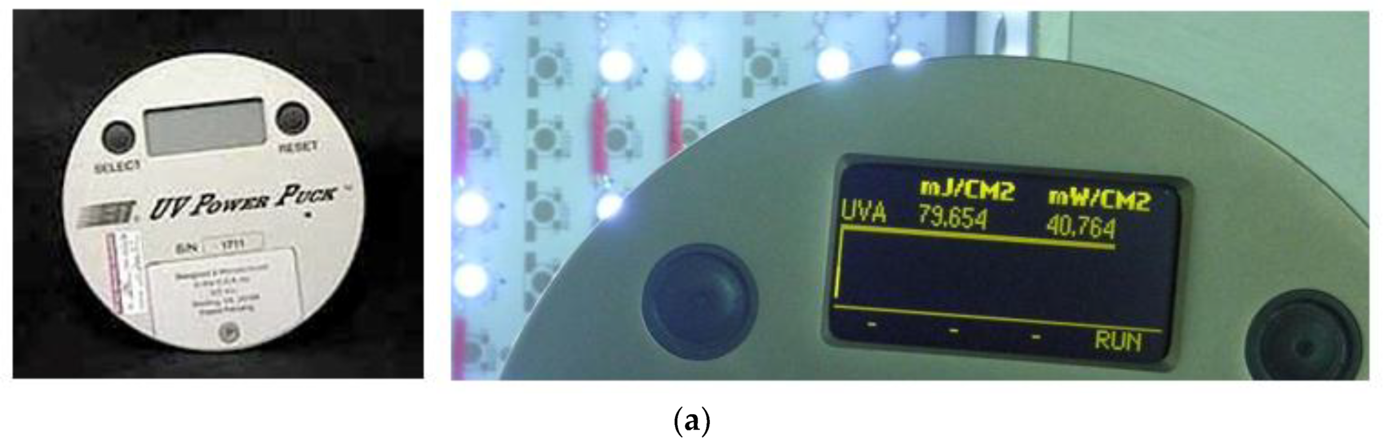
Article

Study of Exposure Uniformity of UV LED Exposure System for Wafer-Level Camera Lenses

1
Tainan Hydraulics Laboratory, National Cheng Kung University, No.500, Sec. 3, Anming Rd., Annan Dist., Tainan City 70955, Taiwan
2
Department of Mechanical Engineering, National Cheng Kung University, No.1, University Road, Tainan 701, Taiwan
3
Department of Engineering Science, National Cheng Kung University, No.1, University Road, Tainan 701, Taiwan
*
Author to whom correspondence should be addressed.
Appl. Sci. 2019, 9(19), 4110; https://doi.org/10.3390/app9194110
Submission received: 30 August 2019 / Revised: 18 September 2019 / Accepted: 26 September 2019 / Published: 1 October 2019
(This article belongs to the Section Applied Industrial Technologies)

Abstract

:
Wafer-level camera lenses are a very promising process for camera lens fabrication. However, there exist some problems with this technology, such as uneven exposure due to curing non-uniformities. In this study, an optical simulation was implemented to simulate the UV light-emitting diodes (LEDs) curing process. We design the LED arrangement, and then find the corresponding LED and adjust the LED power to improve exposure uniformity. The simulation results are very close to the experimental data, and the uniformity is also within the standard range.

1. Introduction

The exposure system is an important part of the semiconductor process, and wafer-level camera lenses are a very promising process for camera lens fabrication, although some problems remain with uneven exposure and non-uniform curing. These problems needed further investigation.
The rapid development of light-emitting diodes (LEDs) over the has surpassed the characteristics of incandescent lamps in luminous efficiency, durability, reliability, safety, and power requirements [1,2]. Although Current high-power LEDs produce up to 120 lm per device, several independent LEDs must be installed on the panel to achieve the actual power. However, in many lighting applications, a uniform illumination distribution is desired, which is affected by the packing density and array configuration of the LEDs [3]. The use of the superposition of illuminance to determine the required interval of the LED array is a good method for designing a lighting system [4,5]. When the panel–target distance is not much longer than the panel size, The illumination non-homogeneity is conspicuous, for example, LED systems that produce directional lighting, such as display lighting [6,7], machine vision [8,9], and microscopy [10].
Moreno et al. [11] analyzed the optimum LED-to-LED spacing. They found the optimum packing density of light sources consisting of multiple LED to uniformly illuminate near targets by considering each single LED as an imperfect Lambertian emitter. They [12] also showed that an array of LED assembled upon a spherical surface can produce a wider angle distribution of light than a typical array and that by arranging every single LED into an optimal placement, the uniformity of the illumination of a target can be improved. Parkyn et al. offer a method [13,14] to design lenses which can change the emission angle of LEDs. The method can increase brightness and luminous efficiency because it makes the beam narrower and concentrated. Kuang et al. [15] proved that the uniformity of illumination can be optimized by reducing the divergence of incident light, as well as adjusting a certain number of columns of the fly-eye lens. Chen W.Z. [16] developed a crystalloid structure with a cone-shape in LED to increase the FWHM angle to 160° and validated this approach with an optical design and simulation software. Chen M.C. [17] presented an exploratory design of a focus-variable UV curing optical system with an LED ring array and studied the influence of the reflector on the UV curing system. Fu W.T. [18] presented an optical design that uses UV LED as the light source and stipulated the utilization rate of light, uniformity, size and working distance. Wu et al. presented a feedback reversing design method [19] improved uniformity of illumination distribution through the design of optical lenses and the computation of the packaging density of LED arrays. Kim et al. proposed an optical design process [20]. The number of LEDs needed to produce the target luminance is calculated from the combined optical efficiencies of the components. Then an appropriate array configuration is sought based on the illuminance distribution function for meeting the target uniformity. Kuo et al. presented a direct LED backlight unit (DLBLU) with extended sources based on an analytical design method [21] of uniform illumination is investigated, and developed an analytical calculation method of the light spread function (LSF) for achieving highly uniform illumination into the diffuser plate of a DLBLU.
In this study, we will be investigating a LED module of an exposure system to do an optical simulation and LED arrangement optimization. We also will add the design of the reflective cover to correct the illumination angle to increase uniformity, then confirming the energy consistency at each point within the effective exposure range to achieve uniformity target.

1.1. Problem Description

After compression molding, the UV curable resin is cured by UV LED. However, in the curing process, the products will not cure uniformly due to the arrangement of the LED. Therefore, this study will use an LED module to carry out an optical simulation and LED arrangement optimization, confirming that the energy consistency at each point is within the effective exposure range.

1.2. Uniformity

Effective energy coverage at each point in the effective exposure range. Measure the intensity or energy of the 9-, 13-, and 25-point positions within the effective exposure range, as calculated by formula (1). The measurement instruments are UV intensity sensor as shown in Figure 1a, the light source is 8 cm away from the UV intensity sensor, and the exposure product has the same placement as the UV intensity sensor. Technical specifications of the UV intensity sensor as shown in Table 1.
1 ( M a x M i n M a x + M i n ) 90 %

2. Materials and Methods

2.1. Simulation Model

In this study, we use the TracePro software to carry out the analysis. In order to reduce the simulation error, we first carried out simulation and experimental verification of a single LED and used the same specification of LED in the experiment. Figure 2 shows an LED model, which can be divided into three parts: substrate, lens, and diode.

LED Scattering Angle

We first confirm the LED lamp scattering angle, and the simulation results in Figure 3 shows this is 141.5 °C, while the actual product specification is 140 °C, as shown in Table 2.
In this study, the reflective cover was set as a perfectly reflective surface, the absorption plate was set as a perfectly absorbing surface, and the uniformity was observed through the absorption plate.

2.2. Parameter Design

LED Spacing Design
The design variables are the distance S1 in the transverse direction, and the vertical distance S2, as shown in Figure 4. We change the spacing between each area to observe the resulting uniformity and luminous intensity. Figure 5a is the type A: 2 × 2 LED area arrangement (a total of 64 LED), while Figure 5b is the type B: 3 × 3 area arrangement (a total of 81 LED).
The simulation condition for the LED power is 134 mW, the reflective cover is set to perfect reflection, the LED spacing is 1 cm, and the distance of the absorption plate and from the LED is 8 cm.
We set the following four parameters in the simulation:
(1) S1 = 0.8 cm, S2 = 0.8 cm; (2) S1 = 0.6 cm, S2 = 0.6 cm; (3) S1 = 0.7 cm, S2 = 0.5 cm; (4) S1 = 0.7 cm, S2 = 0.6 cm.
The simulation results (Figure 6 and Figure 7) show that the use of design variables S1 and S2 does not significantly improve the uniformity (Table 3 and Table 4).
Simulation Results for Type A
Table 3. Uniformity of type A simulation results.
Type AUniformity
variables (1)70.91%
variables (2)68.43%
variables (3)67.22%
variables (4)69.52%
Figure 6. Simulation results of each variable of type A: (a) Results of variables (1), (b) Results of variables (2), (c) Results of variables (3), (d) Results of variables (4).
Applsci 09 04110 g006aApplsci 09 04110 g006b
Simulation Results for Type B
Table 4. Uniformity of type B simulation results.
Type BUniformity
variables (1)71.22%
variables (2)71.51%
variables (3)69.52%
variables (4)70.23%
Figure 7. Simulation results of each variable of type B: (a) Results of variables (1), (b) Results of variables (2), (c) Results of variables (3), (d) Results of variables (4).
Applsci 09 04110 g007aApplsci 09 04110 g007b

2.3. Reflective Cover Design

As the design variables, S1 and S2, do not significantly improve the uniformity, this study changes the reflective cover design. The original reflective cover is a rectangle, and this is then changed to the type shown in Figure 8 to focus the light source, and three designs are simulated:
Type 1: h1 = 1 cm, h2 = 3 cm; Type 2: h1 = 2 cm, h2 = 2 cm; Type 3: h1 = 3 cm, h2 = 1 cm

Reflective Cover Design Simulation Results

We use type B and its simulation conditions to simulate and observe the change in uniformity. It can be seen from the simulation results (Figure 9) that the luminous intensity of reflective cover type 3 is lower than that of the other types, but the uniformity (Table 5) is significantly better, and thus we choose reflective cover type 3 to make subsequent design changes.

3. Results

3.1. Parameter Design Change of Type A

We then change the design variables for type A (Figure 10) to find a better combination. From the previous simulation results, it is known that the current center of the light intensity is too strong.
The design variables are the distance W in the transverse and vertical direction of the center outer area, and the distance D in the transverse and vertical direction of the center area.
The new parameter are as follows:
Type (a): D = 1.44 cm, W = 1.44 cm; Type (b): D = 1.6 cm, W = 1.36 cm; Type (c): D = 2 cm, W = 1.16 cm; Type (d): D = 2.88 cm, W = 0.72 cm. The LED arrangement and simulation results are shown in Figure 11 and Figure 12 and Table 6.
Type (a) is the original design type A, and the results show that the luminous intensity was stronger in the center, so gradually increase the distance D of the center to increase the uniformity. The results show that as D rises, W decreases and evenness increases, with type (d) having the greatest uniformity. This study will thus aim to improve type (d).
Since the previous simulation results show that the center of the light intensity is slightly weak, so we added four LED to the central try and increase this, As shown in Figure 13a and Figure 14a, there is then a significant improvement in uniformity (Table 7).
However, the light intensity of the edge is also observed to be weak, resulting in a decrease in the overall uniformity, as shown in Figure 13b and Figure 14b. We thus removed 4 LED from the central area and found that its uniformity slightly increased. As shown in Figure 13c and Figure 14c, the uniformity increased from 88.47% to 90.34%.
Since the luminous intensity of the central area was still stronger, we removed the eight LED in the surrounding area and found that its uniformity increased significantly, reaching 92.79%, as shown in Figure 13d and Figure 14d.
The results can be summarized as follows:
  • The best type of reflective cover: h1 is 3 cm and h2 is 1 cm. When a smaller h1 value and a larger h2 value are selected, the periphery LED light source is refracted to the central area by the action of the reflector cover, so that the central light intensity is greater than the periphery intensity, and the uniformity is lowered.
  • Increasing the D value can effectively increase the overall uniformity. When the value of D is larger (the number of LEDs in the central area is reduced), the refraction and overlap of the periphery LED light sources do not cause the center intensity too strong.
  • When the above 1. and 2. are executed, the difference between the light intensity of the center and periphery becomes smaller, appropriately increasing the number of LED on the periphery can make the overall uniformity rise.
  • Based on the above simulation results, we use these concepts applied to the design change, type 4 of design change (IV) is a good arrangement in the simulation.
These simulation results can be applied with the actual model arrangement to improve the uniformity.

3.2. Parameter Design Change of Type C

Figure 15 shows the best LED arrangement from the simulation results. The luminous intensity of the central area is still too strong (Figure 16), and the luminous intensity of each corner needs to be strengthened.
In order to increase the uniformity, we reduce the model scale to 1/8, as shown in Figure 16a and Figure 17, to observe the effects of each LED on the overall luminous intensity, and to find which regions need to be improved.
We thus aim to improve the two areas in the center and the upper right corner, as shown in Figure 16b, and find the LED that affects these.
We find the most influential three LED in the upper right corner, as shown in Figure 18. The most influential LED in the center area is shown in Figure 19.
After finding the influential LED, we reduced the LED power on the center area, and increased the LED power on the corner area, with the details shown in Figure 20. The red areas have increased power from 134 to 150 mW, and the blue areas have decreased power from 134 to 120 mW. Figure 21 is the simulation results for these adjusted powers, and the uniformity is 96.72%.

3.3. Simulation of Correction

The previous simulation is mainly to change the LED arrangement and adjust the power of individual LED to greater better uniformity. However, changing the LED arrangement will influence the range of drive power control, so we fixed the LED arrangement and adjusted the LED power per area to improve uniformity. Figure 22 shows the final LED arrangement.
In this LED arrangement model, we divided the area into six regions to adjust the LED power. Figure 23 is the type 1 LED power distribution, and the simulation results are shown in Figure 24. Figure 25 is a comparison of the experimental and simulation results, and these show that the experimental uniformity is 92.52%, and simulation uniformity is 91.97%. The maximum error value of experimental and simulation is about 10%.
We adjusted the power distribution because the light intensity was too strong with the actual products, Figure 26 shows the LED power distribution for the type 2 design.
The simulation results are shown in Figure 27 and compared with the experimental results in Figure 28. The strongest and weakest light intensities are the same positions, the experimental uniformity is 91.8%, and the simulation uniformity is 90.33%. The maximum error value of experimental and simulation is about 13%. Figure 29 is the experimental model of LED power adjustment type 2 in the actual process.

4. Discussion

The model used in the optical analysis was designed based on the experience obtained from the preliminary simulation. In addition to the design variables W and D, the number of LED was also increased in the peripheral area to improve the uniformity. However, the light intensity in the center was still too strong, while that at the edge was too weak. In order to further enhance the overall uniformity, we examined the impact of each LED on the overall light intensity and adjusted the corresponding LED power, thus effectively improving the uniformity.
However, this method is limited by the manufacturer’s power control capabilities. We thus made further advanced design changes, adjusting the LED gap in the center and outer areas, and the LED power distribution per area, to enhance the uniformity. The results showed that this design achieved the uniformity target and was applied to the actual process.
Comparing the experimental and simulated results, the trend of light intensity is generally consistent. Small errors may have been produced due to the material of the reflective cover, as this was set to be perfectly reflective in the simulation.

5. Conclusions

In this study, we used optical simulation to design an LED arrangement to improve exposure uniformity and carried out experimental verification of the actual manufacturing process.
This study showed how to find the areas that need improvement by finding the corresponding LED and adjusting the power. By changing the power of a single LED, as well as their arrangement, we effectively improved the exposure uniformity. However, due to assembly and control difficulties, we choose to simply adjust the LED power per area.
The simulation results are very close to the experimental data, and the uniformity is also within the standard range.

Author Contributions

K.-T.W. researched the literature, conceived the study concepts, designed the simulation method, carried out the simulation, analyzed the simulation results, and took charge of the entire manuscript. S.-J.H. and H.-H.L. assisted with the integrity of the entire study, provided the crucial intellectual support, and revised the manuscript.

Funding

This research received no external funding.

Acknowledgments

The work is supported by Contrel Technology Co., Ltd. and the project title is “Wafer level camera UV curing high precision imprint exposure machine development plan”.

Conflicts of Interest

The authors declare no conflict of interest.

References

  1. Narukawa, Y. White-light LEDs. Opt. Photon. News 2004, 15, 24–29. [Google Scholar] [CrossRef]
  2. Wafer, J. LEDs continue to advance. Photonics Spectra 2005, 39, 60–62. [Google Scholar]
  3. Moreno, I.; Tzonchev, R.I. Effects on Illumination Uniformity Due to Dilution on Arrays of LEDs; Nonimaging Optics and Efficient Illumination Systems: Denver, CO, USA, 2004. [Google Scholar]
  4. Whang, A.J.W.; Chen, Y.Y.; Teng, Y.T. Designing uniform illumination systems by surface-tailored lens and configurations of LED arrays. J. Disp. Technol. 2009, 5, 94–103. [Google Scholar] [CrossRef]
  5. Wang, K.; Wu, D.; Qin, Z.; Chen, F.; Luo, X.; Liu, S. New reversing design method for LED uniform illumination. Opt. Express 2011, 19, A830–A840. [Google Scholar] [CrossRef] [PubMed]
  6. Ito, T.; Okano, K. Color electroholography by three colored reference lights simultaneously incident upon one hologram panel. Opt. Express 2004, 12, 4320–4325. [Google Scholar] [CrossRef] [PubMed] [Green Version]
  7. Yamamoto, H.; Kouno, M.; Muguruma, S.; Hayasaki, Y.; Nagai, Y.; Shimizu, Y.; Nishida, N. Enlargement of viewing area of stereoscopic full-color LED display by use of a parallax barrier. Appl. Opt. 2002, 41, 6907–6919. [Google Scholar] [CrossRef] [PubMed]
  8. Dubovikov, A.L.; Repin, S.S.; Natarovskii, S.N. Features of the use of LEDs in artificial-vision systems. J. Opt. Technol. 2005, 72, 40–42. [Google Scholar] [CrossRef]
  9. Domjan, L.; Kocsanyi, L.; Richter, P.; Varkonyi, S.; Feiten, W. Stripe illuminator based on LED array and parabolic mirror for active triangulation sensors used on mobile robots. Opt. Eng. 2000, 39, 2867–2875. [Google Scholar] [CrossRef]
  10. Repetto, L.; Piano, E.; Pontiggia, C. Lensless digital holographic microscope with Light-Emitting diode illumination. Opt. Lett. 2004, 29, 1132–1134. [Google Scholar] [CrossRef] [PubMed]
  11. Moreno, I.; Avendaño-Alejo, M.; Tzonchev, R.I. Designing Light-Emitting diode arrays for uniform Near-Field irradiance. Appl. Opt. 2006, 45, 2265–2272. [Google Scholar] [CrossRef] [PubMed]
  12. Moreno, I.; Muñoz, J.; Ivanov, R. Uniform illumination of distant targets using a spherical light-emitting diode array. Opt. Eng. 2007, 46, 033001. [Google Scholar]
  13. Parkyn, W.A.; Pelka, D.G. Illuminance-Mapping linear lenses for LEDs. Proc. SPIE Nonimaging Opt. Effic. Illum. Syst. II 2005, 5942, 59420L:1–59420L:12. [Google Scholar]
  14. Parkyn, W.A.; Pelka, D.G. Illumination-Redistribution lenses for Non-Circular spots. Proc. SPIE Nonimaging Opt. Effic. Illum. Syst. II 2005, 5942, 594208:1–594208:12. [Google Scholar]
  15. Kuang, L.J.; Zhai, J.H.; Ruan, Y.; Song, J.M.; Hu, Y. Characteristics of Fly-Eye Lens in Uniform Illumination System. Opt. Optoelectron. Technol. 2005, 6, 29–31. [Google Scholar]
  16. Chen, W.Z. Design and Application for New Ultra-Wide Angle LED Light Source. Master’s Thesis, National Chung Hsing University, Taichung, Taiwan, 2008. [Google Scholar]
  17. Chen, M.C. Optical Design and Development for Focus-Variable UV Curing System. Master’s Thesis, National Chung Hsing University, Taichung, Taiwan, 2012. [Google Scholar]
  18. Fu, W.T. Optical Design and Simulation of High-Performance UV LED Exposure System. Master’s Thesis, National Chung Hsing University, Taichung, Taiwan, 2013. [Google Scholar]
  19. Wu, D.; Wang, K.; Chigrinov, V.G. Feedback reversing design method for uniform illumination in LED backlighting with extended source. J. Disp. Technol. 2014, 10, 43–48. [Google Scholar] [CrossRef]
  20. Kim, B.; Kim, J.; Ohm, W.S.; Kang, S. Eliminating hotspots in a multichip LED array direct backlight system with optimal patterned reflectors for uniform illuminance and minimal system thickness. Opt. Express 2010, 18, 8595–8604. [Google Scholar] [CrossRef] [PubMed]
  21. Kuo, H.K.; Chen, C.F. Design of direct led backlighting based on an analytical method of uniform illumination. J. Disp. Technol. 2016, 12, 1089–1096. [Google Scholar] [CrossRef]
Figure 1. Measuring instruments: (a) EIT UV Power Puck, (b) Model of type A in actual process, (c) The light source is 8 cm away from the UV intensity sensor, and the exposure product has the same placement as it.
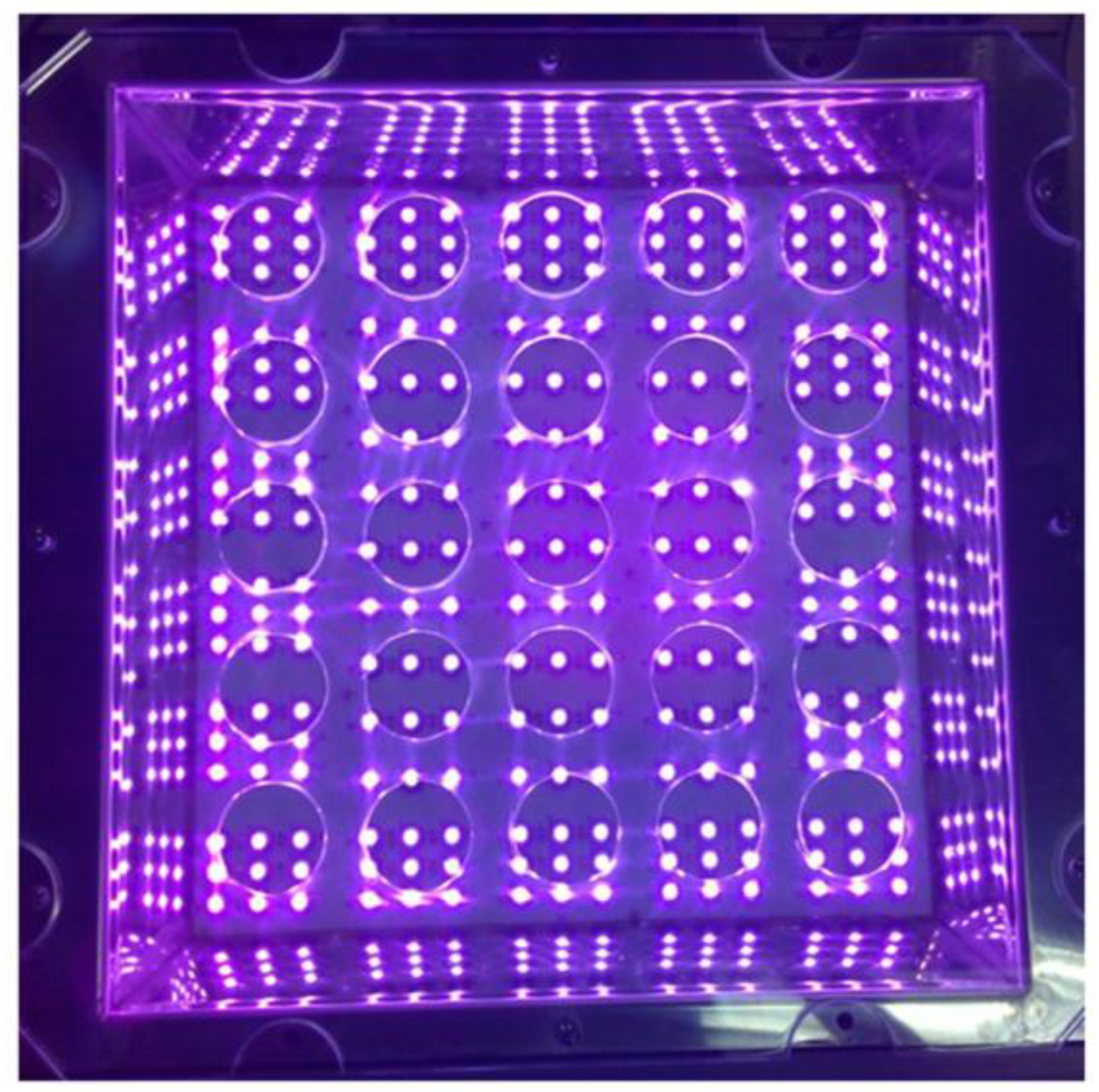
Applsci 09 04110 g001aApplsci 09 04110 g001b
Figure 2. Light-emitting diodes (LEDs) model in simulation.
Applsci 09 04110 g002
Figure 3. LED scattering angle in simulation.
Applsci 09 04110 g003
Figure 4. The design variables S1 and S2.
Applsci 09 04110 g004
Figure 5. Simulation model: (a) type A, (b) type B.
Applsci 09 04110 g005
Figure 8. Reflective cover model.
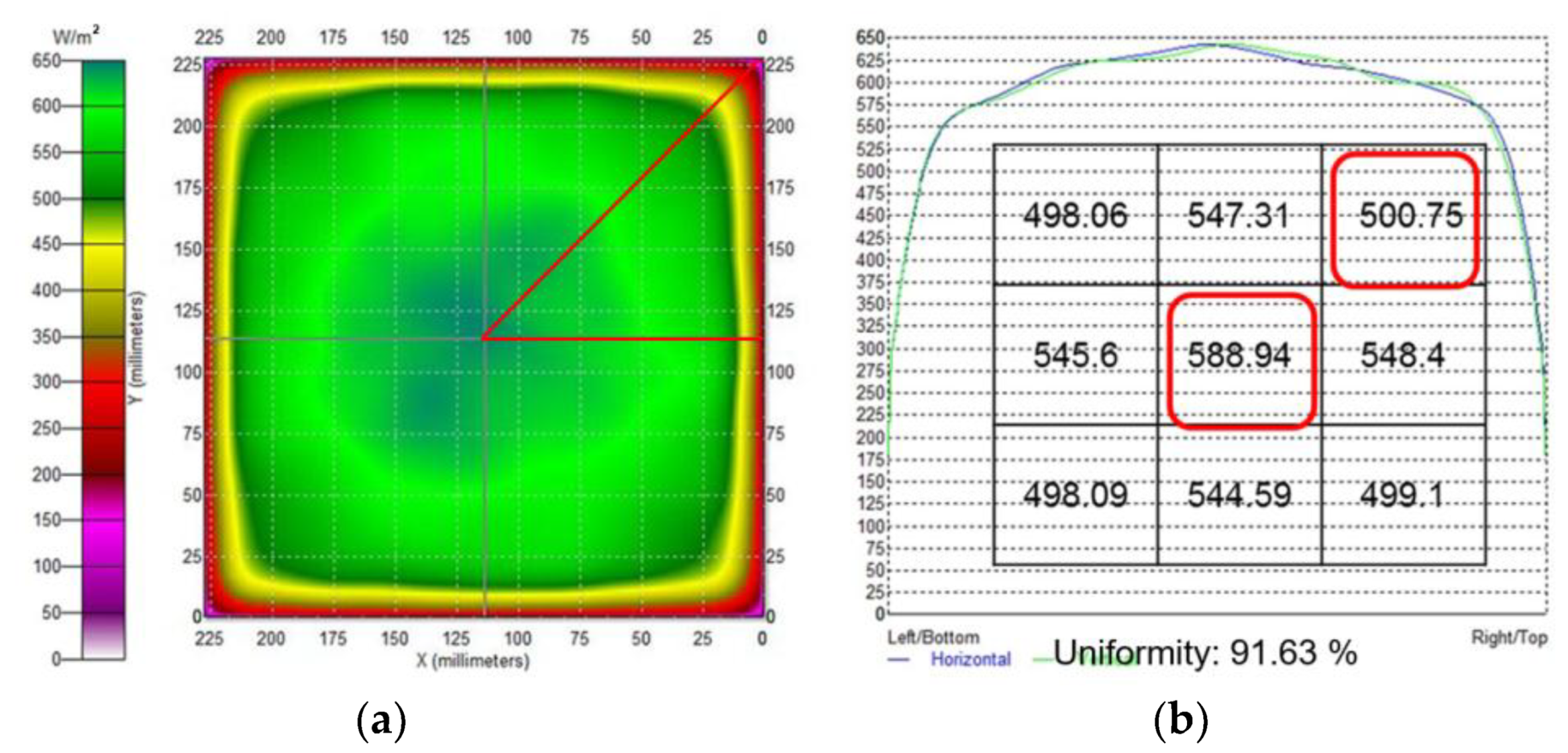
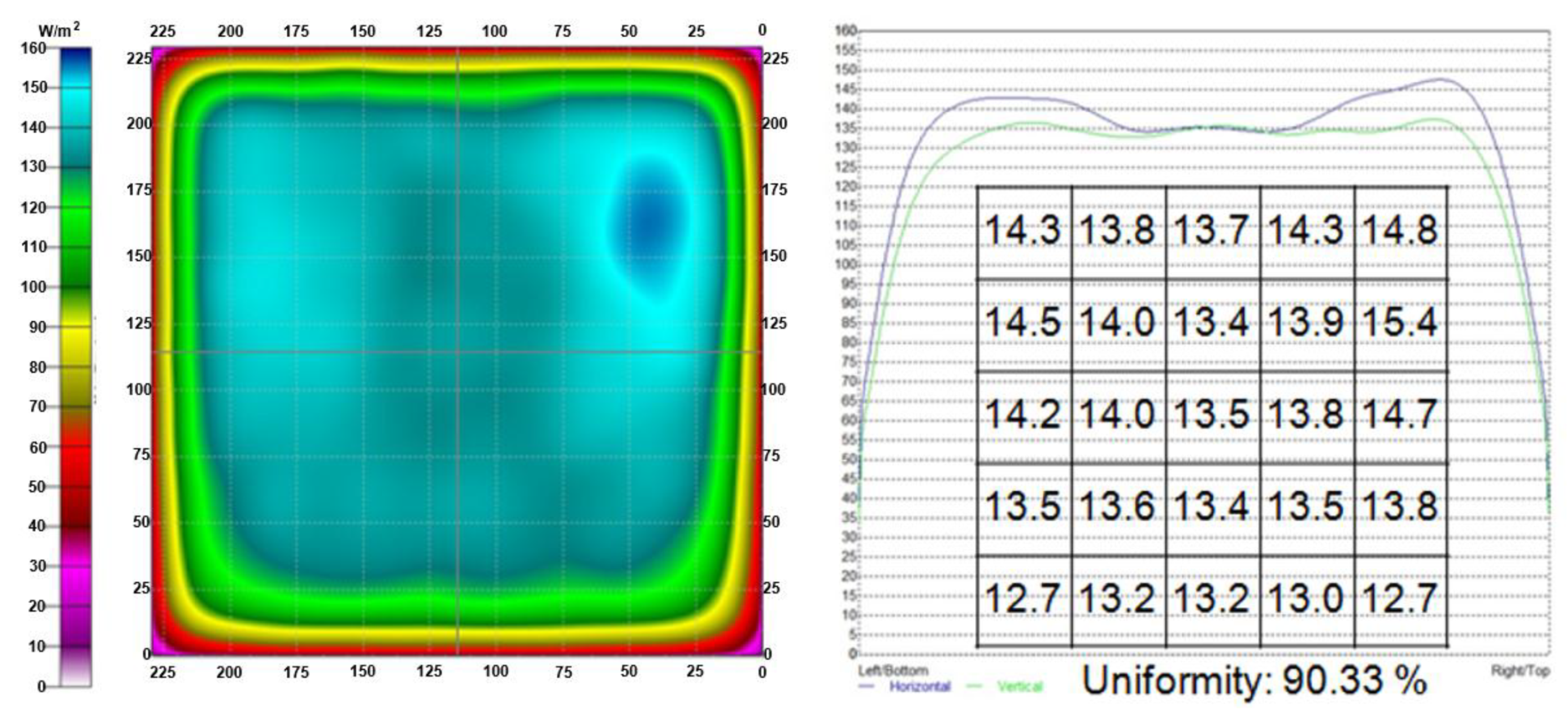
Applsci 09 04110 g008
Figure 9. Simulation results of each reflective cover type: (a) Results of the reflective cover type 1, (b) Results of the reflective cover type 2, (c) Results of the reflective cover type 3.
Applsci 09 04110 g009
Figure 10. Parameter design change model of type A.
Applsci 09 04110 g010
Figure 11. LED arrangement of each type: (a) Type (a), (b) Type (b), (c) Type (c), (d) Type (d).
Applsci 09 04110 g011
Figure 12. Simulation results of each type: (a) Results of type (a), (b) Results of type (b), (c) Results of type (c), (d) Results of type (d).
Applsci 09 04110 g012
Figure 13. LED arrangement of type (d) of each design change: (a) Design change (I), (b) Design change (II), (c) Design change (III), (d) Design change (IV).
Applsci 09 04110 g013
Figure 14. Simulation results of type (d) of each design change: (a) Results of design change (I), (b) Results of design change (II), (c) Results of design change (III), (d) Results of design change (IV).
Applsci 09 04110 g014aApplsci 09 04110 g014b
Figure 15. Model of type C.
Applsci 09 04110 g015
Figure 16. Simulation results of type C: (a) Results of type C, (b) Uniformity of type C.
Applsci 09 04110 g016
Figure 17. The 1/8 model of type C.
Applsci 09 04110 g017
Figure 18. The Influence area (I).
Applsci 09 04110 g018
Figure 19. The Influence area (II).
Applsci 09 04110 g019
Figure 20. The LED power adjustment state.
Applsci 09 04110 g020
Figure 21. Simulation results after adjustment LED power: (a) Results of adjustment LED power, (b) Uniformity of adjustment LED power.
Applsci 09 04110 g021
Figure 22. The final LED arrangement.
Applsci 09 04110 g022
Figure 23. LED power distribution: type 1.
Applsci 09 04110 g023
Figure 24. Simulation results of LED power adjustment type 1.
Applsci 09 04110 g024
Figure 25. (a) The comparison of experimental and simulation of LED power adjustment type 1, (b) The error of experimental and simulation.
Applsci 09 04110 g025
Figure 26. LED power distribution: type 2.
Applsci 09 04110 g026
Figure 27. Simulation results of LED power adjustment type 2.
Applsci 09 04110 g027
Figure 28. (a) The comparison of experimental and simulation of LED power adjustment type 2, (b) The error of experimental and simulation.
Applsci 09 04110 g028
Figure 29. The experimental model of LED power adjustment type 2 in the actual process.
Applsci 09 04110 g029
Table 1. Technical specifications of the UV intensity sensor.
ParameterRange
temperature0~110°
induction spectrumUVA, UVB, UVC, UAA
intensity0~100 mW/cm2
Table 2. LED optical characteristics.
ParameterMin.Max.
Radiant flux15 mW600 mW
Peak wavelength360 nm430 nm
Forward voltage2.8 V4 V
Viewing angle130°150°
Table 5. Uniformity of reflective cover type simulation results.
Reflective CoverUniformity
type 187.84%
type 285.84%
type 390.91%
Table 6. Uniformity of type A of each design variables simulation results.
TypeUniformity
type (a)84.86%
type (b)85.86%
type (c)87.55%
type (d)94.53%
Table 7. Uniformity of type (d) of each design change simulation results.
TypeUniformity
design change (I)89.31%
design change (II)88.47%
design change (III)90.34%
design change (IV)92.79%

