Article

Spatial Resolutions of On-Axis and Off-Axis Transmission Kikuchi Diffraction Methods

1
The State Key Lab of High Performance Ceramics and Superfine Microstructure, Shanghai Institute of Ceramics, Chinese Academy of Science, Shanghai 200050, China
2
Center of Materials Science and Optoelectronics Engineering, University of Chinese Academy of Sciences, Beijing 100049, China
3
CAS Key Laboratory of Mechanical Behavior and Design of Materials, Department of Modern Mechanics, University of Science and Technology of China, Hefei 230027, China
4
Bruker (Beijing) Scientific Technology Co., Ltd., Shanghai 200233, China
*
Authors to whom correspondence should be addressed.
Appl. Sci. 2019, 9(21), 4478; https://doi.org/10.3390/app9214478
Submission received: 18 September 2019 / Revised: 11 October 2019 / Accepted: 19 October 2019 / Published: 23 October 2019
(This article belongs to the Section Applied Physics General)

Abstract

:
Spatial resolution is one of the key factors in orientation microscopy, as it determines the accuracy of grain size investigation and phase identification. We determined the spatial resolutions of on-axis and off-axis transmission Kikuchi diffraction (TKD) methods by calculating correlation coefficients using only the effective parts of on-axis and off-axis transmission Kikuchi patterns. During the calculation, we used average filtering to evaluate the spatial resolution more accurately. The spatial resolutions of both on-axis and off-axis TKD methods were determined in the same scanning electron microscope at different accelerating voltages and specimen thicknesses. The spatial resolution of the on-axis TKD was higher than that of the off-axis TKD at the same parameters. Furthermore, with an increase in accelerating voltage or a decrease in specimen thickness, the spatial resolutions of the two configurations could be significantly improved, from tens of nanometers to below 10 nm. At a voltage of 30 kV and sample thickness of 74 nm, both on-axis and off-axis TKD methods exhibited the highest resolutions of 6.2 and 9.7 nm, respectively.

1. Introduction

Electron back-scattering diffraction (EBSD) is a powerful technique in material science for microstructural analyses [1]. The use of nanomaterials has rapidly increased with the development of nanotechnologies. Nevertheless, the limited spatial resolution of the EBSD may not be sufficient to reveal the substructures and this may hamper its application in nanomaterial analyses.
To improve the spatial resolution of the EBSD, Keller and Geiss changed the EBSD configuration so that the Kikuchi patterns formed by transmitted electrons can be acquired [2]. The resultant electron diffraction technique is referred to as transmission EBSD or off-axis transmission Kikuchi diffraction (off-axis TKD). However, the pattern center is distant from the center of the detector in the off-axis TKD method, which leads to a considerable distortion. In 2016, Fundenberger et al. proposed an on-axis TKD method, in which the incident beam, sample, and detector are collinear [3]. Compared to the off-axis TKD, the new configuration provides higher signal intensity and lower distortion. Furthermore, either the electron dose or acquisition time can be reduced 20 times to yield an equivalent pattern quality as that in the off-axis TKD method [4,5,6].
In recent years, both off-axis and on-axis TKD methods have been extensively used to analyze nanocrystalline and ultrafine-grain materials [6,7,8,9,10,11]. The spatial resolution is one of the key factors in the EBSD-based orientation microscopy, as it determines the accuracy of grain size investigations and phase identifications. Although Kikuchi patterns are commonly used to provide two-dimensional information about the microstructure of a material, they are a product of the three-dimensional electron interaction volume [12]. Consequently, when the electron beam is scanned across a grain boundary, the interaction volumes of both sides overlap, which leads to overlapping and unindexable Kikuchi patterns. Zaefferer defined two types of spatial resolution, physical spatial resolution (PSR) and effective spatial resolution (ESR) [13]. The PSR corresponds to the smallest distance from a large-angle grain boundary where the overlapping pattern of both crystals appears, while the ESR indicates the smallest distance across a boundary where the patterns are still indexable by a software algorithm [13,14]. Niessen et al. compared the on-axis and off-axis TKD methods in many aspects, including the spatial resolution [5]. They investigated the effect of working distance in spatial resolution at detector-typical microscope parameters and demonstrated that the PSR of the on-axis TKD was slightly improved compared to that of the off-axis TKD. However, no extensive studies have been carried out on the PSR changes with other microscope parameters and sample parameters for on-axis and off-axis TKDs in the same scanning electron microscope (SEM). In addition, the low signal-to-noise ratio of the TKD pattern leads to errors in the calculation of the PSR, which has been neglected in previous research.
In this study, the evaluation method for the PSR was improved by considering only the effective parts of the patterns, while the noisy parts were eliminated during the calculation. Additionally, we introduced average filtering to remove low-frequency noise, and thus, precisely calculate the spatial resolution. Furthermore, the spatial resolution difference between the off-axis and on-axis TKDs was investigated at different accelerating voltages and specimen thicknesses. We aimed to analyze the limitations of the instruments for an optimal analysis of each sample.

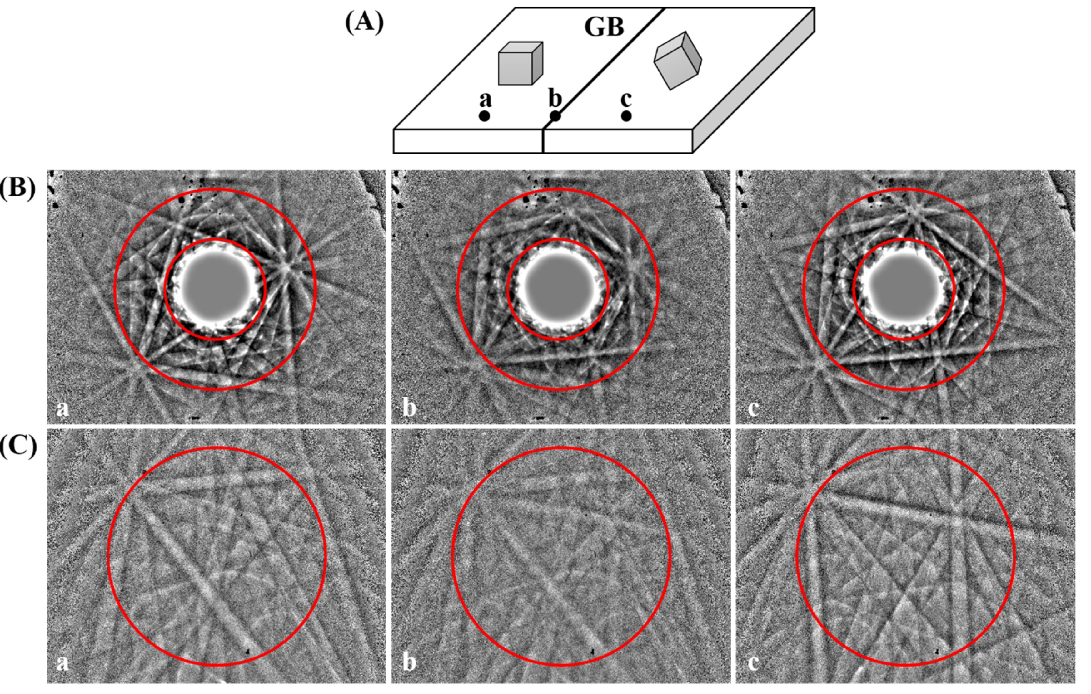
2. Materials and Methods

2.1. Sample Preparation

To measure the spatial resolutions of the on-axis and off-axis TKD methods, an electron-transparent sample containing twin boundaries is needed. Ferritic steel was used in this study for this purpose. The sample was polished with a 1200-grit abrasive paper. Subsequently, diamond suspensions were used for mechanical polishing. Afterwards smooth finishing was carried out by ion milling by using a LEICA EM TIC 3X system (Leica Mikrosysteme GmbH, Vienna, Austria). During the ion milling, voltages of 5.5 kV and 4.5 kV were used for polishing.
The polished sample was cut using a dual focused ion beam system in FEI Versa™ 3D SEM (FEI, Brno, Czech Republic). Before cutting, platinum was deposited on the surface of the sample to protect it from damage. The grain boundary of the sample was identified in a back-scatter electron channeling image. Subsequently, an area with both grains and boundaries was selected and cut off from the matrix. The sample was welded onto a copper holder for further thinning. Three samples were cut from the same twin boundary to ensure that the boundary width was the same. They were thinned to three different thicknesses by a low Ga ion current of 100 pA and a low voltage of 3 kV, which was also applied to remove the amorphous layer. Finally, the thicknesses of the three samples were evaluated by the platinum layer deposited on the surface using a back-scatter electron image. Five measurements were taken for each sample to obtain an average thickness; these were 169 ± 1 nm, 91 ± 1 nm, 74 ± 2 nm.

2.2. TKD

Both on-axis and off-axis TKD spatial resolutions were measured by using a TESCAN MIRA3 SEM (TESCAN, Brno, Czech Republic) equipped with a Bruker eFlashFS detector. For the off-axis TKD, the sample stage was tilted by −20° and the scintillator was set in the vertical position. For the on-axis TKD, a Bruker OPTIMUS™ detector head (Bruker Nano GmbH, Berlin, Germany) was set horizontally, and the tilt angle was set to 0°. During the measurements in both configurations, the spot size was set to 4.8 nm. The operation and detector distances were 5 and 14.2 mm, respectively. The image resolution of all Kikuchi patterns was 640 × 480 pixels, while the contrast was 3%. To ensure a good pattern quality, the beam current and exposure time in the on-axis and off-axis TKD measurements were set to 1 nA and 70 ms, and 2 nA and 150 ms, respectively. All samples were oriented so that their grain boundaries were parallel to the incident electron beam and perpendicular to the scanning direction. The Kikuchi pattern at each step was recorded while the beam was scanned across the grain boundary at accelerating voltages of 20–30 kV with increments of 5 kV and scanning step of 2 nm.

3. Results and Discussion

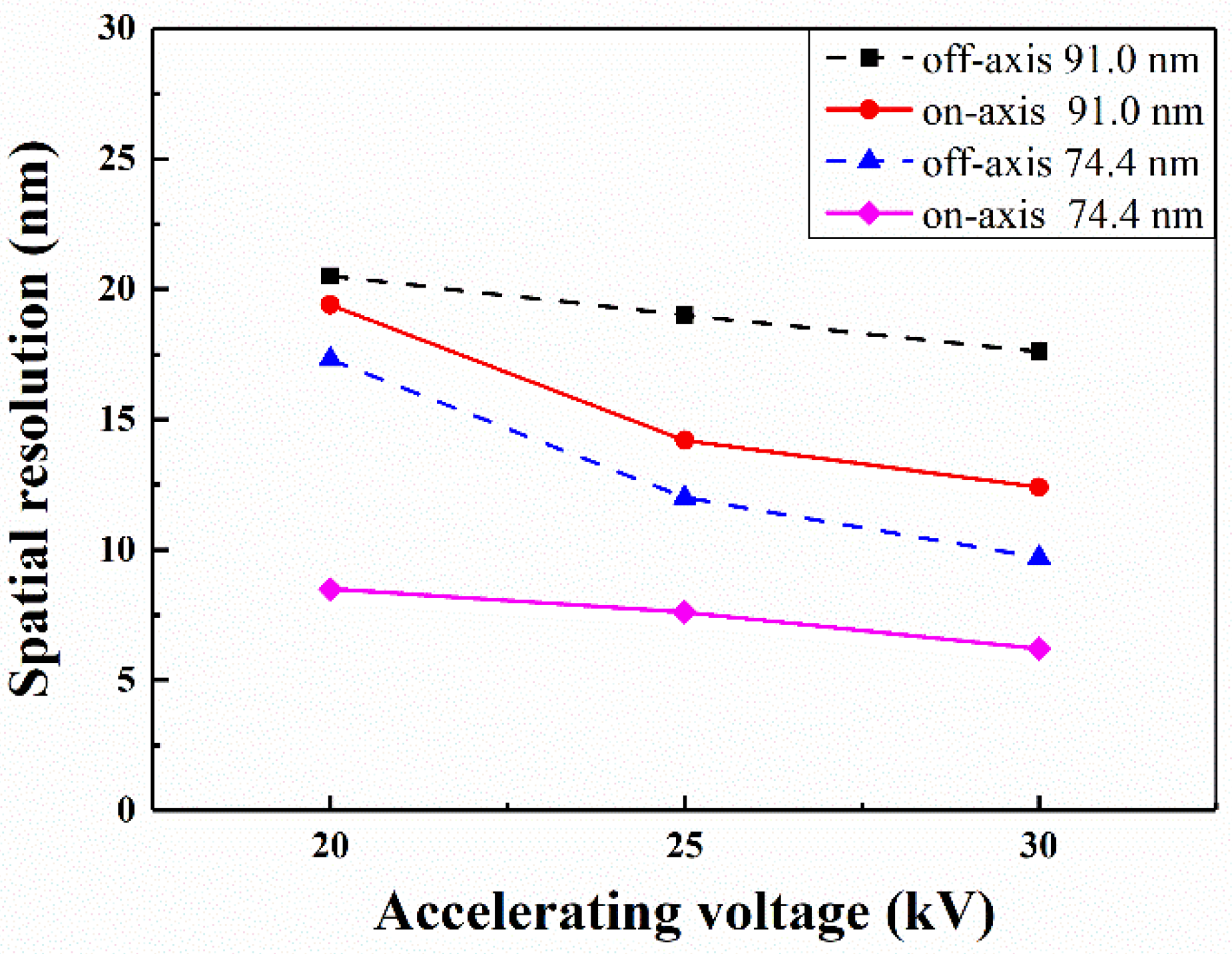
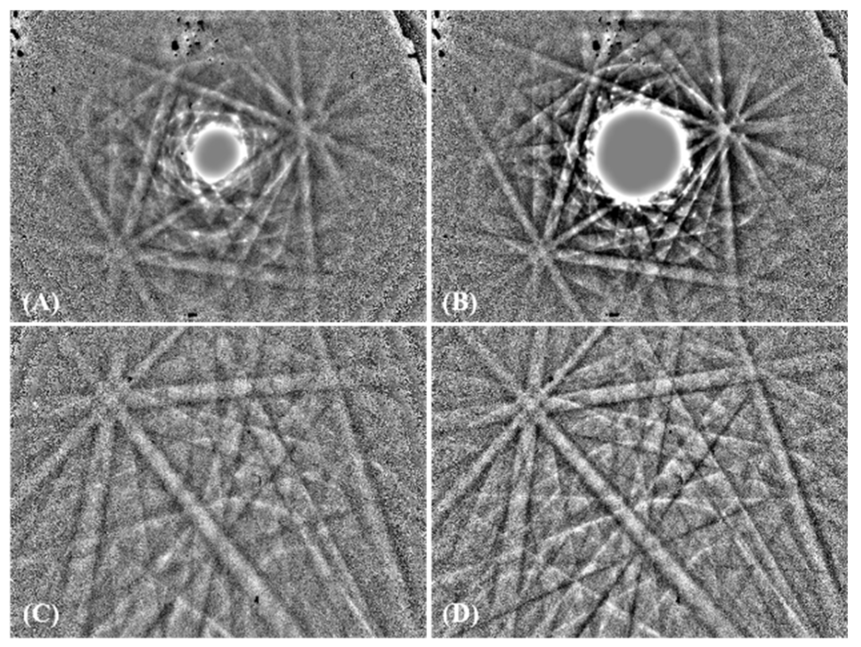
3.1. Quantitative Evaluation of the Spatial Resolution

In this study, the digital image correlation (DIC) technique [15,16,17] was used to investigate the effects of the accelerating voltage and specimen thickness. The DIC method can be used to quantitatively evaluate small variations between patterns by calculating their correlation coefficient. As the electron beam is scanned close to a grain boundary, the interaction volumes of both sides overlap, which leads to overlapping Kikuchi patterns, and thus to a decreased correlation coefficient. Therefore, this method can be used to determine the spatial resolution. It has been extensively used to evaluate the physical resolutions of the EBSD [14,18] and off-axis TKD methods [19,20,21]. The correlation coefficient can be expressed as r i j = g i j g ¯ i j g i j 2 g ¯ i j 2 , where g i j and g ¯ i j denote the grey scale of the reference and sampling pattern at each position (i,j), respectively.
The middle part of the on-axis and off-axis Kikuchi patterns have good qualities; however, the boundaries of the patterns contain considerable noise. Moreover, a bright spot is generated by the transmitted beam in the center of the on-axis Kikuchi pattern. The size and shape of the bright spot can change during the scanning. Thus, if the whole pattern (640 × 480 pixels) is considered, the correlation coefficient would deviate and the results would be inaccurate. Therefore, regions of interest (ROIs) have to be selected to increase the precision. Wang et al. used this method to determine the resolution of the off-axis TKD [19]. In this study, we have used a similar approach. Circular ROIs were chosen for the off-axis TKD, which contained the overlapping region, as shown in Figure 1C. On the other hand, annular ROIs were selected in the on-axis TKD to ensure that the boundaries and bright spots were eliminated while retaining the overlapping regions (Figure 1B). In addition, the chosen ROIs should be as large as possible to ensure representativity.
The calculated correlation coefficients at a voltage of 30 kV and specimen thickness of 91 nm are presented in Figure 2. Chen et al. [14] and Shih et al. [20] applied a fast Fourier transform (FFT) filter to reduce the noise, while FFT followed by inverse FFT were applied by Wang et al. [19] to obtain smooth curves. FFT is commonly used for filtering in the frequency domain; if a smooth profile is needed, the peak may be broadened. Therefore, an average filtering algorithm is introduced to avoid the deviation in the correlation coefficient, which can smooth profiles in the spatial domain. As it does not affect the profile width, it is commonly used to filter out Gaussian noise. In Figure 2B, the low-frequency noise was removed and the whole curve became smoother after filtering. The smooth profiles of the correlation coefficients were summed and normalized. The procedure is presented in previous reports [14,19,20]. With this approach, we can obtain the sum of the normalized correlation coefficients as a function of the distance (Figure 2C) and the full width at half maximum can be easily calculated, which is defined as the PSR [14].

3.2. Difference in Spatial Resolution between the On-Axis and Off-Axis TKD Methods

By using the above method, the spatial resolutions of the on-axis and off-axis TKD methods were measured in the same SEM at the same sample position. The data obtained at different voltages and sample thicknesses are presented in Figure 3. The intensity and contrast of the pattern for the 169-nm-thick sample were too low to identify at the same parameters used for the other two samples. Therefore, results are presented only for the two samples.
The spatial resolution of the on-axis TKD was better than that of the off-axis TKD at the same accelerating voltage and thickness; the largest gap was 8 nm. The only difference between the two configurations was the intersection angle between the phosphor screen and incident beam (α) [5]. In the off-axis TKD, the intersection angle had a magnitude of only a few degrees, which led to a high gnomonic distortion and low diffraction intensity. On the contrary, no pattern distortion and high diffraction intensity were observed in the on-axis TKD because the angle α was close to 90°. Consequently, in the off-axis TKD, the probe current and/or exposure time have to be increased to produce an equivalent pattern quality. In this study, we increased both current and exposure time. Nonetheless, the increase in current leads to larger probe size and interaction volume, which inevitably increase the spatial resolution. Therefore, at their optimal parameters, the beam current used in the off-axis TKD method should be higher than that in the on-axis TKD method, which leads to a larger spatial resolution. Similarly, if we set equal parameters for both TKD methods, the pattern quality in the off-axis TKD method would be worse owing to its lower intensity. Therefore, the spatial resolution of the off-axis TKD would still be worse than that of the on-axis TKD.
Another reason for the difference is the smaller net scattering angle in the on-axis TKD because of the detector geometry. At a given depth, the path length through the sample is smaller for the on-axis TKD, which implies that fewer scattering events may occur before the electrons reach the detector. Therefore, the on-axis TKD has a thicker source region of detected intensity, which is beneficial to the lateral spatial resolution, but detrimental to the depth spatial resolution [5,22].

3.3. Effects of the Accelerating Voltage and Specimen Thickness on the On-Axis and Off-Axis TKDs

As shown in Figure 3, the spatial resolutions of both configurations were improved, from tens of nanometers to below 10 nm, with the increase in accelerating voltage or decrease in sample thickness. At the voltage of 30 kV and sample thickness of 74 nm, the on-axis and off-axis TKD methods achieved the lowest resolutions of 6.2 and 9.7 nm, respectively.
With the increase in thickness, the Kikuchi bands became less sharp and higher noises were observed at the boundaries of the patterns. For the on-axis TKD, the size of the direct beam decreased with the increase in thickness, which indicates a larger energy loss before the electrons emerge from the sample (Figure 4). The results also demonstrate that a thinner sample leads to a better spatial resolution. If the thickness is reduced by only tens of nanometers, the spatial resolution would be significantly improved. This can be explained by the scattering events of diffracted electrons along the crystal plane [19,21,23,24]. For the same material at the same accelerating voltage, the electron penetration depth is the same. If the sample is thicker, the electron point source would be further from the emergence surface. This increases the likelihood of incoherent scattering along the emergence path, which leads to a larger energy loss and reduced pattern contrast [8,25]. On the other hand, less scattering events lead to a smaller electron beam broadening, and thus to a lower spatial resolution. Usually, the thickness of the TKD sample should be 1.5 times the grain size. If the specimen thickness is more than two times the grain size, the Kikuchi patterns of the top and bottom layers would overlap. This would lead to a significantly reduced pattern quality. The minimum thickness for TKD is a quarter of the extinction distance, according to Rice et al. [24], because the total number of scattering events will be rapidly reduced and the scattering angle will be very small, below the threshold.
With the increase in accelerating voltage, the width of the Kikuchi band decreases and the boundary becomes clearer. For the on-axis TKD, the transmitted-beam diameter and diffraction spot brightness are increased (Figure 5). The spatial resolution can be improved by increasing the accelerating voltage; however, the influence of the voltage on the spatial resolution is reduced above 25 kV. In other words, if the accelerating voltage is sufficiently high so that most electrons reach the detector, the spatial resolution will be minimally affected by the voltage. When the acceleration voltage is 30 kV, the spatial resolution is optimal, which can also be explained by scattering events. According to a Monte Carlo simulation, the electron penetration depth increases with the accelerating voltage [20]. Therefore, for a material with the same thickness, the point source will be closer to the emergence surface. This indicates fewer scattering events will happen before the electrons leave the sample because of the shorter path, which leads to better spatial resolution. However, in both configurations, the accelerating voltage has a minor role in the spatial resolution compared to that of the specimen thickness.
The results are in agreement with our previous study on the spatial resolutions of the off-axis TKD method for 41-, 69-, and 91-nm-thick austenitic steel samples [19]. Nevertheless, the spatial resolution measured in this study is considerably lower for the samples with a similar thickness, mainly because of the improved filtering algorithm. Furthermore, the density of the ferritic steel is lower than that of the austenitic steel. According to van Bremen et al., TKD is more effective in the analyses of less dense samples [23]. Additionally, Wang et al. reported that the spatial resolution at a voltage of 20 kV and thickness of 91 nm could not be calculated owing to the low intensity. In contrast, we evaluated the resolution under the same conditions, because the current in the off-axis TKD was 2 nA, instead of 1.6 nA, as used by Wang et al.

4. Conclusions

The spatial resolutions of the on-axis and off-axis TKD methods were investigated by the improved DIC technique. We considered only the effective parts of the patterns and eliminated the noisy parts during the calculation to reduce the deviation. Moreover, average filtering was used to remove the low-frequency noise. The spatial resolution of the on-axis TKD was better than that of the off-axis TKD at the same accelerating voltage and sample thickness, which was attributed mainly to the high intensity and thick source region in the on-axis TKD. Furthermore, the spatial resolutions of both configurations were improved with an increase in accelerating voltage or a decrease in sample thickness. The optimal resolutions were achieved at the voltage of 30 kV and sample thickness of 74 nm, 6.2 nm for the on-axis TKD and 9.7 nm for the off-axis TKD.

Author Contributions

Conceptualization, Y.Z.; methodology, Y.S., Y.Z., Y.W., J.Z. and B.Y.; software, J.X.; formal analysis, Y.S.; investigation, Y.S.; writing—original draft preparation, Y.S.; writing—review and editing, Y.S.; supervision, Y.Z. and Hong Miao; project administration, Y.Z.; funding acquisition, Y.Z.

Funding

This research was funded by the National Key R&D Program of China (2018YFB0704400), CAS Key Foundation for Exploring Scientific Instrument (YJKYYQ20170041), International Partnership Program of Science (GJH21721), Shanghai Technical Platform for testing on inorganic materials (19DZ2290700), and Shanghai Action Projects for Scientific and Technological Innovation (17142201500).

Acknowledgments

The authors are grateful for the technical assistance provided by Xuemei Song, Ziwei Liu, Chucheng Lin, Wei Zheng, Caifen Jiang and Henghui Cai.

Conflicts of Interest

The authors declare no conflict of interest.

References

  1. Wright, S.I.; Nowell, M.M.; Lindeman, S.P.; Camus, P.P.; De Graef, M.; Jackson, M.A. Introduction and comparison of new EBSD post-processing methodologies. Ultramicroscopy 2015, 159, 81–94. [Google Scholar] [CrossRef] [PubMed] [Green Version]
  2. Keller, R.R.; Geiss, R.H. Transmission EBSD from 10 nm domains in a scanning electron microscope. J. Microsc. 2012, 245, 245–251. [Google Scholar] [CrossRef]
  3. Fundenberger, J.J.; Bouzy, E.; Goran, D.; Guyon, J.; Yuan, H.; Morawiec, A. Orientation mapping by transmission-SEM with an on-axis detector. Ultramicroscopy 2016, 161, 17–22. [Google Scholar] [CrossRef] [PubMed]
  4. Yuan, H.; Brodu, E.; Chen, C.; Bouzy, E.; Fundenberger, J.J.; Toth, L.S. On-axis versus off-axis Transmission Kikuchi Diffraction technique: Application to the characterisation of severe plastic deformation-induced ultrafine-grained microstructures. J. Microsc. 2017, 267, 70–80. [Google Scholar] [CrossRef] [PubMed]
  5. Niessen, F.; Burrows, A.; Fanta, A.B.d.S. A systematic comparison of on-axis and off-axis transmission Kikuchi diffraction. Ultramicroscopy 2018, 186, 158–170. [Google Scholar] [CrossRef] [Green Version]
  6. Brodu, E.; Bouzy, E.; Fundenberger, J.-J.; Guyon, J.; Guitton, A.; Zhang, Y. On-axis TKD for orientation mapping of nanocrystalline materials in SEM. Mater. Charact. 2017, 130, 92–96. [Google Scholar] [CrossRef]
  7. Trimby, P.W. Orientation mapping of nanostructured materials using transmission Kikuchi diffraction in the scanning electron microscope. Ultramicroscopy 2012, 120, 16–24. [Google Scholar] [CrossRef]
  8. Brodusch, N.; Demers, H.; Gauvin, R. Nanometres-resolution Kikuchi patterns from materials science specimens with transmission electron forward scatter diffraction in the scanning electron microscope. J. Microsc. 2013, 250, 1–14. [Google Scholar] [CrossRef]
  9. Trimby, P.W.; Cao, Y.; Chen, Z.; Han, S.; Hemker, K.J.; Lian, J.; Liao, X.; Rottmann, P.; Samudrala, S.; Sun, J.; et al. Characterizing deformed ultrafine-grained and nanocrystalline materials using transmission Kikuchi diffraction in a scanning electron microscope. Acta Mater. 2014, 62, 69–80. [Google Scholar] [CrossRef]
  10. Liu, Z.W.; Hua, J.J.; Lin, C.C.; Jiang, C.F.; Zeng, Y. Application of Transmission Electron Backscattered Diffraction in Nanomaterials Research. J. Inorg. Mater. 2015, 30, 833–837. [Google Scholar]
  11. Proust, G.; Trimby, P.; Piazolo, S.; Retraint, D. Characterization of Ultra-fine Grained and Nanocrystalline Materials Using Transmission Kikuchi Diffraction. Jove-J. Vis. Exp. 2017. [Google Scholar] [CrossRef] [PubMed]
  12. Sorensen, C.; Basinger, J.A.; Nowell, M.M.; Fullwood, D.T. Five-Parameter Grain Boundary Inclination Recovery with EBSD and Interaction Volume Models. Metall. Mater. Trans. A 2014, 45, 4165–4172. [Google Scholar] [CrossRef]
  13. Zaefferer, S. On the formation mechanisms, spatial resolution and intensity of backscatter Kikuchi patterns. Ultramicroscopy 2007, 107, 254–266. [Google Scholar] [CrossRef] [PubMed]
  14. Chen, D.; Kuo, J.-C.; Wu, W.-T. Effect of microscopic parameters on EBSD spatial resolution. Ultramicroscopy 2011, 111, 1488–1494. [Google Scholar] [CrossRef] [PubMed]
  15. Isabell, T.C.; Dravid, V.P. Resolution and sensitivity of electron backscattered diffraction in a cold field emission gun SEM. Ultramicroscopy 1997, 67, 59–68. [Google Scholar] [CrossRef]
  16. Dingley, D. Progressive steps in the development of electron backscatter diffraction and orientation imaging microscopy. J. Microsc. Oxf. 2004, 213, 214–224. [Google Scholar] [CrossRef] [PubMed]
  17. Ren, S.X.; Kenik, E.A.; Alexander, K.B.; Goyal, A. Exploring spatial resolution in electron back-scattered diffraction experiments via Monte Carlo simulation. Microsc. Microanal. 1998, 4, 15–22. [Google Scholar] [CrossRef]
  18. Chen, D.; Kuo, J.-C. The Effect of Atomic Mass on the Physical Spatial Resolution in EBSD. Microsc. Microanal. 2013, 19, 4–7. [Google Scholar] [CrossRef] [Green Version]
  19. Wang, Y.Z.; Kong, M.G.; Liu, Z.W.; Lin, C.C.; Zeng, Y. Effect of microscope parameter and specimen thickness of spatial resolution of transmission electron backscatter diffraction. J. Microsc. 2016, 264, 34–40. [Google Scholar] [CrossRef]
  20. Shih, J.-W.; Kuo, K.-W.; Kuo, J.-C.; Kuo, T.-Y. Effects of accelerating voltage and specimen thickness on the spatial resolution of transmission electron backscatter diffraction in Cu. Ultramicroscopy 2017, 177, 43–52. [Google Scholar] [CrossRef]
  21. Kuo, C.-W.; Kuo, J.-C.; Wang, S.-C. Resolution of transmission electron backscatter diffraction in aluminum and silver: Effect of the atomic number. Ultramicroscopy 2018, 193, 126–136. [Google Scholar] [CrossRef] [PubMed]
  22. Sneddon, G.C.; Trimby, P.W.; Cairney, J.M. Transmission Kikuchi diffraction in a scanning electron microscope: A review. Mater. Sci. Eng. R 2016, 110, 1–12. [Google Scholar] [CrossRef]
  23. Van Bremen, R.; Ribas Gomes, D.; de Jeer, L.T.H.; Ocelik, V.; De Hosson, J.T.M. On the optimum resolution of transmission-electron backscattered diffraction (t-EBSD). Ultramicroscopy 2016, 160, 256–264. [Google Scholar] [CrossRef] [PubMed]
  24. Rice, K.P.; Keller, R.R.; Stoykovich, M.P. Specimen-thickness effects on transmission Kikuchi patterns in the scanning electron microscope. J. Microsc. 2014, 254, 129–136. [Google Scholar] [CrossRef] [PubMed] [Green Version]
  25. Went, M.R.; Winkelmann, A.; Vos, M. Quantitative measurements of Kikuchi bands in diffraction patterns of backscattered electrons using an electrostatic analyzer. Ultramicroscopy 2009, 109, 1211–1216. [Google Scholar] [CrossRef] [PubMed]
Figure 1. (A) Schematic of the ferritic steel lamella used for the determination of the spatial resolutions of the on-axis and off-axis transmission Kikuchi diffraction (TKD). Kikuchi patterns across the grain boundary at an accelerating voltage of 30 kV and thickness of 91 nm, acquired by (B) on-axis TKD (the regions of interest (ROIs) are outlined by the red annular rings) and (C) off-axis TKD (the ROIs are outlined by the red circles).
Applsci 09 04478 g001
Figure 2. Correlation coefficient profiles at the accelerating voltage of 30 kV and thickness of 91 nm (A) determined by using the digital image correlation (DIC) technique by comparing the sampling patterns with the left (blue curve) and right patterns (red curve) in order and (B) after average filtering. (C) Sum of the normalized correlation coefficients as a function of the distance.
Applsci 09 04478 g002
Figure 3. Spatial resolution of the on-axis and off-axis TKD methods as functions of the accelerating voltage at thicknesses of 91 and 74 nm.
Applsci 09 04478 g003
Figure 4. Kikuchi patterns at the accelerating voltage of 30 kV and thicknesses of (A,C) 91 and (B,D) 169 nm for the on-axis and off-axis TKDs, respectively. These two samples are presented because the difference in their thickness is larger.
Applsci 09 04478 g004
Figure 5. Kikuchi patterns of the 91-nm-thick sample at the voltages of (A,C) 20 and (B,D) 30 kV for the on-axis and off-axis TKDs, respectively.
Applsci 09 04478 g005

