Abstract
Photogeneration of excess charge carriers in semiconductors produces electronic strain. Under transient conditions, electron-hole pairs may be separated across a potential barrier. Using time-resolved X-ray diffraction measurements across an intrinsic AlGaAs/n-doped GaAs interface, we find that the electronic strain is only produced by holes, and that electrons are not directly observable by strain measurements. The presence of photoinduced charge carriers in the n-doped GaAs is indirectly confirmed by delayed heat generation via recombination.
1. Introduction
Deformation potential theory was originally developed by Bardeen and Shockley [1] to describe the interactions between thermal electrons and acoustic vibrational modes in non-polar crystals. It was initially used to explain the dependence of electrical conductivity on pressure. The theory also predicts a dependence of the energy band gap upon dilation; changes in energy band structure consequently result in changes in carrier concentration. This effect of the deformation potential has been exploited in several applications such as strain transducers [2]. It was soon realized that the deformation potential effect can be inverted to explain the generation of electronic strain by charge carriers in cubic semiconductors [3],
where is the pressure dependence of the energy gap and is the density of photogenerated electron-hole pairs. Studies of photogenerated electronic strain have been undertaken using modulated laser beams to produce photo-acoustic waves [4] as well as by direct imaging of opticaly-excited semiconductors in a scanning probe microscope [5]. In some materials the electronic strains can be quite large; for instance [4] found the electronic strain in Silicon irradiated with 514.5 nm laser light was 2.6 times larger than the strain generated by thermal expansion under the same conditions.
The deformation potential can be either negative or positive. In crystal Silicon is negative (contractile), whereas in crystal Gallium Arsenide is positive (tensile) [6] and therefore also results in expansion similar to thermal strain. In the past two decades, it has become recognized that the deformation potential often plays a dominant role in the lattice dynamics of semiconductor materials following ultrafast laser excitation [7,8,9,10,11]. In many of these studies, such as the one presented here, small transient changes in lattice spacing can be resolved by high-resolution synchrotron X-ray diffraction, and the logarithmic range of timescales probed can be exploited along with depth or material sensitivity to disentangle the transport of heat, sound, and charge in bulk or heterostructure crystals.
Although both the direction and magnitude of the deformation potential has been calculated and measured in many materials of interest, it is generally assumed that the charge carriers are electron-hole pairs and exist locally in equal concentrations [6]. To the best of our knowledge, the contributions of the individual species (electrons or holes) to electronic strain have never been directly distinguished. As time-resolved X-ray Scattering (TRXS) techniques continue to improve temporal and spatial resolution (e.g., [12,13]), it will become routine to explore charge transport across heterojunctions. This interest is motivated in part by the desire to control semiconductor properties via strain for optimizing devices, especially optoelectronic devices with large concentrations of photogenerated charge carriers. Therefore, we have performed a time-resolved X-ray diffraction measurement to directly observe the effects of photogenerated electrons alone in crystalline GaAs. As shown in Figure 1, an ultrashort pulse of above-bandgap laser light is absorbed on the surface of an intrinsic (undoped) AlGaAs layer that was epitaxially grown on top of a n-doped GaAs substrate. A cap layer, buffer layer, and ohmic metal contacts were used to ensure that the sample remained highly conductive (50 across the entire device) so that the photocarriers could easily move through the AlGaAs layer to the buried i-n interface which serves as a potential barrier to holes, but a potential drop to electrons. Electrons will therefore cross the interface into the n-GaAs, and eventually either exit the device through a matched load or recombine in the substrate while leaving the holes behind in the intrinsic AlGaAs. Although AlGaAs and GaAs have very different electronic bandgaps, their thermo-acoustic properties are very similar and they have lattice constants that are sufficiently different (≈0.1%) to be resolved as separate X-ray diffraction peaks. We find surprisingly that the electronic strain does not transport across the interface along with the electrons, indicating that holes are primarily responsible for electronic strain.
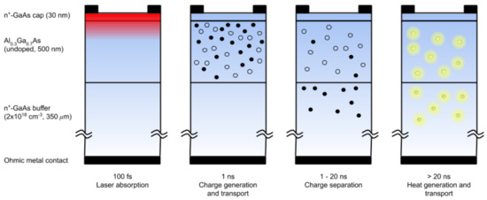
Figure 1.
The multilayer i-n sample is shown with dynamics at each timescale. The blue-shaded region represents the X-ray extinction depth of 1.5 m. The red-shaded 400 nm laser only penetrates approximately 100 nm into the intrinsic AlGaAs layer, which has a bandgap of 2.0 eV. Both electrons (solid circles) and holes (empty circles) are generated withing the laser excitation volume and by 1 ns have diffused throughout the intrinsic layer. Only majority carriers (electrons) may penetrate into the n-doped GaAs, which has a bandgap of 1.5 eV. Eventually, charge scattering and recombination generate heat (shaded in yellow).
2. Materials and Methods
The experiments were performed at the sector 7ID insertion device beamline at the Advanced Photon Source (APS) and PAL-KRISS 1C time-resolved beamline at Pohang Light Source-II. The schematics of the TRXS setup is shown in Figure 2, of which details is elaborated elsewhere [14]. X-rays from a water cooled double-crystal diamond (1 1 1) monochromator combined with horizontal-plane focusing and vertical slits provided a collimated, 50-micron square beam profile on the sample mounted at the center of a four-circle diffractometer allowing femtometer spatial sensitivity. During the standard operational mode of the X-ray sources, the temporal resolution is approximately 100 ps full width half maximum (FWHM). This time-resolution is sufficient to study charge dynamics, since the deformation potential results in long-lasting elastic deformation of the crystal from charges. Using this capability, we mapped out the temporal evolution of the inter-atomic spacing along the crystal surface direction at different time-delays between an 400-nm wavelength, 100-fs optical-pump and 10-KeV X-ray probe pulses. For the sample, the 500-nm thick AlGaAs thin film was grown on the n-type doped (2 × 10 cm) GaAs substrate by molecular beam epitaxy and capped with a very thin protective GaAs layer. The multilayer sample is oriented in the symmetric (0 0 4) Bragg reflection geometry at ambient temperature for the time-resolved measurement.
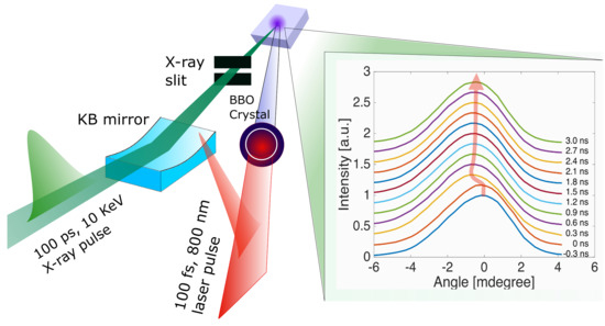
Figure 2.
Experimental configuration. Monochromatic synchrotron X-ray pulses (green) are focused horizontally by a dynamically-bent mirror, while the vertical dimension is slit to preserve angular resolution. The synchronized amplified laser pulse is focused and then frequency doubled in a BBO crystal to 400 nm before overlapping the X-ray beam on the sample. A gated Avalanche Photodiode in proportional detection mode and digital oscilloscope [15] are used to record high dynamic-range rocking curves over several hundred X-ray pulses at the laser’s 1 kHz repetition rate. Rocking curves are repeated as the laser-to-X-ray delay is scanned by introducing electronic delays via a phase shifter in the phase locked loop that maintains synchronization. The centroid of the peak is used to determine average strain and after several ns following electron recombination, the average temperature of the layer.
3. Results
Figure 3a shows the Bragg diffraction peaks arising from the film and the substrate layers of the sample. The angular separation between the two peaks implies the lattice mismatch less than () between the layers. The oscillatory intensity signatures between the Bragg peaks is due to interference between X-rays diffracted from the side bands of the film and substrate peaks. We are able to estimate the film thickness of 500 nm from the oscillation period that is found consistent with the sample design. Figure 3b,c show symmetric (0 0 4) Bragg diffraction curves from the heterostructure sample at selected time-points relative to the optical excitation at an absorbed fluence of 3 mJ/cm. The vertical axis is the relative time-delay between the X-ray and the laser pulses and the horizontal axis represents the X-ray incidence angle. Under the kimematical diffraction approximation, the resulting average lattice displacements can be extracted by converting the angular diffraction shifts, , to changes in the lattice parameter, , using Bragg’s law, , where is the X-ray wavelength and and are the temporally evolving crystal lattice spacing and Bragg diffraction angle, respectively. Such transient deviation in the diffraction condition represent the aggregate lattice conditions over the finite X-ray extinction depth of 1.5 m, and thus provides averaged changes in the lattice spacing for both the film and the substrate layers.

Figure 3.
The time-resolved X-ray scattering can be angularly separated into the top AlGaAs laser and lower GaAs substrate. The fringe separation shown in (a) are consistent with the 500 nm layer thickness. The initial response is shown in (b) where an impulsive strain wave begins in the film and moves at the longitudinal speed of sound into the substrate [16]. Panel (c) shows the complex carrier dynamics occuring in the intrinsic AlGaAs film within the first several ns, but with no discernible electronic strain in the substrate.
Here, we discuss the information that can be directly inferred from the measured transient strains in both layers. Initially, the AlGaAs layer shows marginal compression followed by rapid expansion after the photoexcitation, of which behavior is expected from a bipolar wave propagating away from the surface. The rise of the initial tensile response reaching its maximum within 100 ps corresponds to the transit time of the longitudinal acoustic wave propagating out of the film thickness of 500 nm. In meantime, the GaAs layer gets compressed and then expanded reaching the peak lattice displacement at about = 500 ps. The disparities between the lattice behaviors between the two layers within 1-ns time-scale can be explained in terms of an elastic response consisting of two counter-propagating compression waves that are generated by instantaneous expansion of the AlGaAs surface due to electron-hole plasma [17]. Since the timescale of the charge carrier diffusion across the film layer is comparable to that of the acoustic-transit time, it is reasonable to assume that the tensile effect in the film layer is caused by sum of electronic strain driven by deformation potential, thermalized lattice (heat) and sound wave propagation. Within the acoustic and electronic timescales (<5 ns) in the substrate, we only observe the impulsive lattice response generated by the sound wave propagation, or transient compression followed by expansion. Tensile electronic strain would be evidenced by monotonically increasing strain, and is not observed at early times.
Following these early timescale dynamics, the tensile strain the AlGaAs layer continuously increases until = 25 ns and proceeds to decrease toward its equilibrium as shown in Figure 4a. On the other hand, the lattice in the substrate increases at a considerably slow rate prolonging up to approximately = 200 ns, at which point the amplitudes of the tensile displacement from the film and the substrate crosses. Afterwards, the GaAs substrate remains more expanded throughout the entire cooling process indicating that the substrate layer has become the heat source.
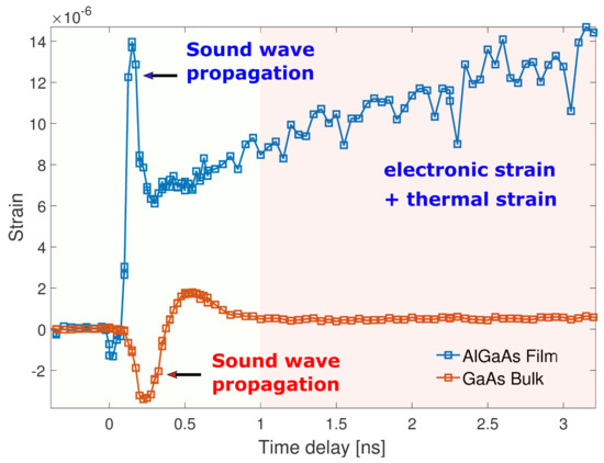
Figure 4.
Centroid shifts of AlGaAs (blue) and GaAs (red) taken from Figure 2. Only impulsive sound wave propogation is observed in the GaAs bulk at early times.
4. Discussion
Above-band gap excitation on the surface of the AlGaAs film leads to instantaneous creation of electron-hole plasma. As they diffuse into the bulk, they impart their energy to lattice via electron-phonon scattering to generate heat and non-thermal processes such as deformation potential (DP) coupling. Consequently, the temporal evolution of the free charge carrier distribution results in generating various forms of transient strains until the free-carrier dynamics evolve towards equilibrium. In particular, the DP contribution is intimately linked to the free carrier concentration and can be used to trace its evolution. Due to symmetric sample geometry, we are only sensitive to the DP coupling and thermal expansion of the lattice. By monitoring the temporal evolution of the Bragg peak shifts, we follow propagation of strain across X-ray probe depth into the depth direction. As shown in Figure 4, the general trend of the peak movements in early timescales ( < 200 ns) shows that the excess energy (large strain) flows from the film layer into the substrate. Subsequently, both layers come to a near equilibrium state at much longer timescale of several hundreds of nanoseconds.
In Figure 5a, a few nanoseconds should allow sufficient time for free electron-hole pairs to diffuse away from the film surface and traverse across the epitaxial interface introducing the effect of the DP coupling driven lattice expansion in the substrate. However, aside from the impulsive lattice response due to the sound wave propagation, we do not measure any additional contribution of tensile strain until thermal diffusion takes place in the substrate. Apparent lack of tensile strain within intermediate timescales (few nanoseconds) implies that strain measurement is indeed insensitive to the presence of optically induced free electron population.
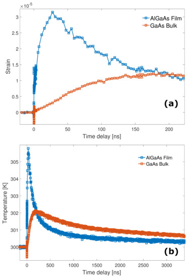
Figure 5.
(a) Shifts of the diffraction peak centroid are used to determine average strains in the AlGaAs film (blue) and GaAs substrate (red). The average film strain increases to half-maximum in 10 ns, comparable to a calculated thermal time transit of ns across the nm film thickness where the thermal diffusion constant of AlGaAs is m/s. Temperature rises across the n-doped GaAs substrate to half-maximum in 40 ns, comparable to the 1.5 m X-ray extinction (probe) depth estimated diffusion time of 35 ns. In (b) these average layer strains are converted into temperatures using thermal expansion coefficients. The bulk remains warmer longer than the film, indicating that charge carriers are indeed present generating heat and transporting back into the X-ray penetration depth.
It can be inferred from our result that only mobile electrons have migrated into the substrate (i.e., lack of holes), of which excess energy is used to generate heat via electron-phonon coupling. Consequently, the substrate becomes hotter than the initially excited layer, effectively making it a secondary heating source. Assuming that the electrons have thermalized with the lattice at sufficiently long time-scales (>hundreds of nanoseconds), we can convert the lattice strain into temperature based on Bragg’s law using the thermal expansion coefficient of the materials as shown in Figure 5b. We note that the apparent temperature offset between the two layers implies a non-negligible thermal boundary resistance even for an epitaxially-grown interface [18]. However, evaluating the exact value of the thermal boundary resistance would require additional data sets at different laser fluence and elaborate modeling of the strain evolution based on dynamical X-ray diffraction theory [19,20], which is beyond the scope of present study.
5. Conclusions
The intrinsic AlGaAs/n-doped interface provides a barrier to hole transport, allowing the electronic strain from electrons and holes to be separated following a sudden injection of photo-carriers into the intrinsic material. Unlike the electron-hole pairs and holes left behind in the top intrinsic layer, the electrons appear invisible as they move throughout the n-doped substrate. Their presence is only detected much later as their recombination results in delayed heating of the substrate. It is unclear why only the holes contribute to electronic strain, but it may be due to the interpretation that (especially in positive deformation potential materials such as GaAs) the removal of an electron from the valence band weakens the crystal structure, leading to expansion. Species-specific electronic strains will need to be taken into account when analyzing electron transport across heterojunctions and may impact the design of semiconductor light detectors, strain transducers, and light sources.
Author Contributions
Conceptualization, S.L. and E.C.L.; methodology, all authors; software, W.J., S.L., S.S. and E.C.L; writing—original draft preparation, S.L. and E.C.L.; writing—review and editing, E.C.L., S.L. and T.P.H.
Funding
E.C.L. was supported by a DePaul CSH FSRG. This research used resources of the Advanced Photon Source, Sector 7ID-C, a U.S. Department of Energy (DOE) Office of Science User Facility operated for the DOE Office of Science by Argonne National Laboratory under contract No. DE-AC02-06CH11357. This research was supported by the National Research Foundation of Korea under contract No. NRF-2019K1A3A7A09033397).
Acknowledgments
We acknowledge assistance in data collection from Grace Longbons and and Ellie D. Martin-Eberhardt; data analysis assistance from Sinead Humphrey, X-ray operations assistance from Donald Walko, and laser operations assistance from Haiden Wan; sample preparation by S.J. Lee at KRISS; use of PAL-KRISS beamline at PLS-II for preliminary sample measurement.
Conflicts of Interest
The authors declare no conflict of interest.
References
- Bardeen, J.; Shockley, W. Deformation Potentials and Mobilities in Non-Polar Crystals. Phys. Rev. 1950, 80, 72–80. [Google Scholar] [CrossRef]
- Habermehl, C.L.; Newell, J.T. Electronic Pressure-Sensitive Semiconductor Device. U.S. Patent 3,470,392, 30 September 1969. [Google Scholar]
- Figielski, T. Photostriction effect in germanium. Physica Status Solidi (B) 1961, 1, 306–316. [Google Scholar] [CrossRef]
- Stearns, R.; Kino, G. Effect of electronic strain on photoacoustic generation in silicon. Appl. Phys. Lett. 1985, 47, 1048–1050. [Google Scholar] [CrossRef]
- Takata, K.; Nakasuji, S.; Nishino, T.; Osaka, R.; Matsushita, Y. Photo-induced strain imaging of semiconductors. AIP Adv. 2017, 7, 045104. [Google Scholar] [CrossRef]
- Wei, S.H.; Zunger, A. Predicted band-gap pressure coefficients of all diamond and zinc-blende semiconductors: Chemical trends. Phys. Rev. B 1999, 60, 5404. [Google Scholar] [CrossRef]
- Baumberg, J.; Williams, D.; Köhler, K. Ultrafast acoustic phonon ballistics in semiconductor heterostructures. Phys. Rev. Lett. 1997, 78, 3358. [Google Scholar] [CrossRef]
- Lindenberg, A.; Kang, I.; Johnson, S.L.; Missalla, T.; Heimann, P.; Chang, Z.; Larsson, J.; Bucksbaum, P.; Kapteyn, H.; Padmore, H.; et al. Time-resolved X-ray diffraction from coherent phonons during a laser-induced phase transition. Phys. Rev. Lett. 2000, 84, 111. [Google Scholar] [CrossRef] [PubMed]
- Lee, S.; Cavalieri, A.; Fritz, D.; Swan, M.; Hegde, R.; Reason, M.; Goldman, R.; Reis, D. Generation and propagation of a picosecond acoustic pulse at a buried interface: Time-resolved X-ray diffraction measurements. Phys. Rev. Lett. 2005, 95, 246104. [Google Scholar] [CrossRef] [PubMed]
- Williams, G.J.; Lee, S.; Walko, D.A.; Watson, M.A.; Jo, W.; Lee, D.R.; Landahl, E.C. Direct measurements of multi-photon induced nonlinear lattice dynamics in semiconductors via time-resolved X-ray scattering. Sci. Rep. 2016, 6, 39506. [Google Scholar] [CrossRef] [PubMed]
- Lee, S.; Williams, G.J.; Campana, M.I.; Walko, D.A.; Landahl, E.C. Picosecond X-ray strain rosette reveals direct laser excitation of coherent transverse acoustic phonons. Sci. Rep. 2016, 6, 19140. [Google Scholar] [CrossRef] [PubMed]
- Jo, W.; Landahl, E.C.; DiChiara, A.D.; Walko, D.A.; Lee, S. Measuring femtometer lattice displacements driven by free carrier diffusion in a polycrystalline semiconductor using time-resolved X-ray scattering. Appl. Phys. Lett. 2018, 113, 032107. [Google Scholar] [CrossRef]
- Pudell, J.; Maznev, A.A.; Herzog, M.; Kronseder, M.; Back, C.H.; Malinowski, G.; von Reppert, A.; Bargheer, M. Layer specific observation of slow thermal equilibration in ultrathin metallic nanostructures by femtosecond X-ray diffraction. Sci. Rep. 2018, 9, 3335. [Google Scholar] [CrossRef] [PubMed]
- Dufresne, E.M.; Adams, B.; Arms, D.A.; Chollet, M.; Landahl, E.C.; Li, Y.; Walko, D.A.; Wang, J. Time-Resolved Research at the Advanced Photon Source Beamline 7-ID. AIP Conf. Proc. 2010, 1234, 181–184. [Google Scholar]
- Williams, G.J.; Watson, M.A.; Arms, D.A.; Mooney, T.M.; Walko, D.A.; Landahl, E.C. EPICS oscilloscope for time-resolved data acquisition. Nucl. Instrum. Methods Phys. Res. Sect. A Accel. Spectrom. Detect. Assoc. Equip. 2011, 649, 84–86. [Google Scholar] [CrossRef]
- Thomsen, C.; Grahn, H.T.; Maris, H.J.; Tauc, J. Surface generation and detection of phonons by picosecond light pulses. Phys. Rev. B 1986, 34, 4129. [Google Scholar] [CrossRef] [PubMed]
- DeCamp, M.F.; Reis, D.A.; Cavalieri, A.; Bucksbaum, P.H.; Clarke, R.; Merlin, R.; Dufresne, E.; Arms, D.; Lindenberg, A.M.; MacPhee, A.; et al. Transient strain driven by a dense electron-hole plasma. Phys. Rev. Lett. 2003, 91, 165502. [Google Scholar] [CrossRef] [PubMed]
- Sheu, Y.; Lee, S.; Wahlstrand, J.; Walko, D.; Landahl, E.; Arms, D.; Reason, M.; Goldman, R.; Reis, D. Thermal transport in a semiconductor heterostructure measured by time-resolved X-ray diffraction. Phys. Rev. B 2008, 78, 045317. [Google Scholar] [CrossRef]
- Wie, C.; Tombrello, T.T.; Vreeland, T., Jr. Dynamical X-ray diffraction from nonuniform crystalline films: Application to X-ray rocking curve analysis. J. Appl. Phys. 1986, 59, 3743–3746. [Google Scholar] [CrossRef]
- Stepanov, S. Method of transfer matrices and dynamical thick-crystal approximation in surface X-ray diffraction by multilayer structures. Crystallogr. Rep. 1994, 39, 182–187. [Google Scholar]


© 2019 by the authors. Licensee MDPI, Basel, Switzerland. This article is an open access article distributed under the terms and conditions of the Creative Commons Attribution (CC BY) license (http://creativecommons.org/licenses/by/4.0/).