Review

Micro-Raman Mapping of the Strain Field in GaAsN/GaAsN:H Planar Heterostructures: A Brief Review and Recent Evolution

Dipartimento di Fisica, Università degli Studi di Pavia, 27100 Pavia, Italy
*
Author to whom correspondence should be addressed.
Appl. Sci. 2019, 9(22), 4864; https://doi.org/10.3390/app9224864
Submission received: 18 September 2019 / Revised: 24 October 2019 / Accepted: 8 November 2019 / Published: 13 November 2019
(This article belongs to the Special Issue Novel Insights to Raman Spectroscopy: Advances and Prospects)

Abstract

:

Featured Application

Micro-Raman mapping can provide detailed information about the strain distribution in GaAsN/GaASN:H planar heterostructures.

Abstract

Raman scattering is an effective tool for the investigation of the strain state of crystalline solids. In this brief review, we show how the analysis of the GaAs-like longitudinal optical phonon frequency allowed to map the strain behavior across interfaces in planar heterostructures consisting of GaAsN wires embedded in GaAsN:H matrices. Moreover, we recently showed how the evolution of the longitudinal optical frequency with increasing H dose strongly depends on polarization geometry. In a specific geometry, we observed a relaxation of the GaAs selection rules. We also present new results which demonstrate how laser irradiation intensity–even at low levels–may affect the line shape of the GaAs-like spectral features in GaAsN hydrogenated materials.

1. Introduction

It is well known that Raman scattering is an effective tool in detecting the strain state in crystalline solids [1,2] and binary semiconductors, such as GaAs, under stress [3,4]. Besides mechanical stress, other fields may induce strain in a crystal, which in turn can modify the frequency of lattice modes. This is the case of Fe-doped Lithium Niobate. In this crystal, the photorefractive electric field—that can be produced by the Raman probe itself—can induce such a strain via the piezoelectric effect. As a result, a shift in Raman modes can be detected [5]. The phonon deformation potentials (PDP) are the rates of change of long-wavelength optical phonon frequencies with strain. The sensitivity of phonon frequencies to the strain state can be exploited via PDP not only in bulk materials, but also in layers and even heterostructures. An example of special interest is that of the GaAs1-xNx alloy [6,7] grown as a pseudomorphic layer on top of GaAs buffer, where the reduced lattice parameter of the alloy results in the development of a biaxial tensile strain in the layer [6,7,8,9]. The incorporation of hydrogen via irradiation makes the lattice parameter increase up to the value of GaAs, or even beyond, eventually leading to the buildup of compressive strain [8,9,10].
In fact, it is now well established that hydrogen almost completely neutralizes the effect of nitrogen on the band structure of the GaAs host matrix via the formation of nitrogen-hydrogen complexes N-nH (with n = 2, 3) [8,9,10,11,12,13,14]. The redshifted band gap E- blueshifts toward the typical energy position in GaAs materials. On the other hand the E+ band disappears after hydrogen irradiation [8,9,10] and the photoreflectance (PR) spectra of the H-treated GaAsN layers closely resemble (broad) GaAs spectra [8,15]. At the same time, after hydrogenation, the GaAs-like Raman features near 292 cm−1 persist. In contrast, the Ga-N local vibrational mode (LVM), near 475 cm−1, disappears [8].
The GaAs-like Raman modes are only weakly perturbed by hydrogenation. Nevertheless, the longitudinal optical (LO) phonon frequency exhibits a blueshift (of the order of 1 cm−1 or less) which is indicative of a reduction of the native biaxial tensile strain of the untreated material [8]. In fact, the frequency shift of the GaAs-like LO mode can be usefully applied for monitoring the strain state of GaAsN layers in planar heterostructures, as reported for GaAsN wires separated by GaAsN:H barriers [16].
This approach may be effective in improving the design of planar heterostructures for light polarization control obtained by selective H-irradiation of dilute nitride semiconductors [11]. In fact, spatially selective hydrogenation [17] can be used to engineer the strain profile and, hence, the mixing of heavy hole and light hole valence-band states. This allows tuning of the optical properties of the material. In particular, by realizing arrays of GaAsN/GaAsN:H wires at different orientations [18], a high degree of linear polarization was achieved for the light emitted by the sample. On the other hand, the same approach can be used to get a deeper insight (on a microscale) on the strain modulation ensuing the formation of N-nH complexes in the patterned GaAsN/GaAsN:H structures. In particular, it was shown that the formation of N-2H complexes (typical of early stage of the hydrogenation process) produces, besides N passivation, near-perfect lattice-matching with the GaAs buffer layer. On the other hand, N-3H centers are related to a sizeable “overshooting” of the lattice parameter of the host material, and consequently induce strain inversion in the H irradiated GaAsN layers [17,18,19,20,21]. If detailed and accurate knowledge of the strain profile derived from Raman map analysis is available, it will reliably compare with results from Finite-Elements calculations, thus serving as a method to check the strain profile in the heterostructure.
As far as other suggested applications are concerned, it is remarkable that one can realize heterostructures in which untreated and hydrogenated GaAsN are characterized by a ~2% refractive index mismatch over a broad spectral interval that comprises the 1.3 and 1.55 µm telecommunications windows [12]. Such mismatch is sufficient to confine light and fabricate optical waveguides [17,22].
In this paper, we firstly recall the main features of the experimental and analytical procedure successfully applied to a previously well-characterized sample for strain field mapping in GaAsN/GaAsN:H planar heterostructures, then we shall discuss the possibility of optically determining the uniaxial strain at the wire-barrier interface by an appropriate data reduction method. Finally, the effects of H dose, experimental polarization geometries, and excitation power on the line shape and frequencies of the Raman structures will be addressed.

2. Experimental and Analytical Procedure

2.1. Optical Mapping
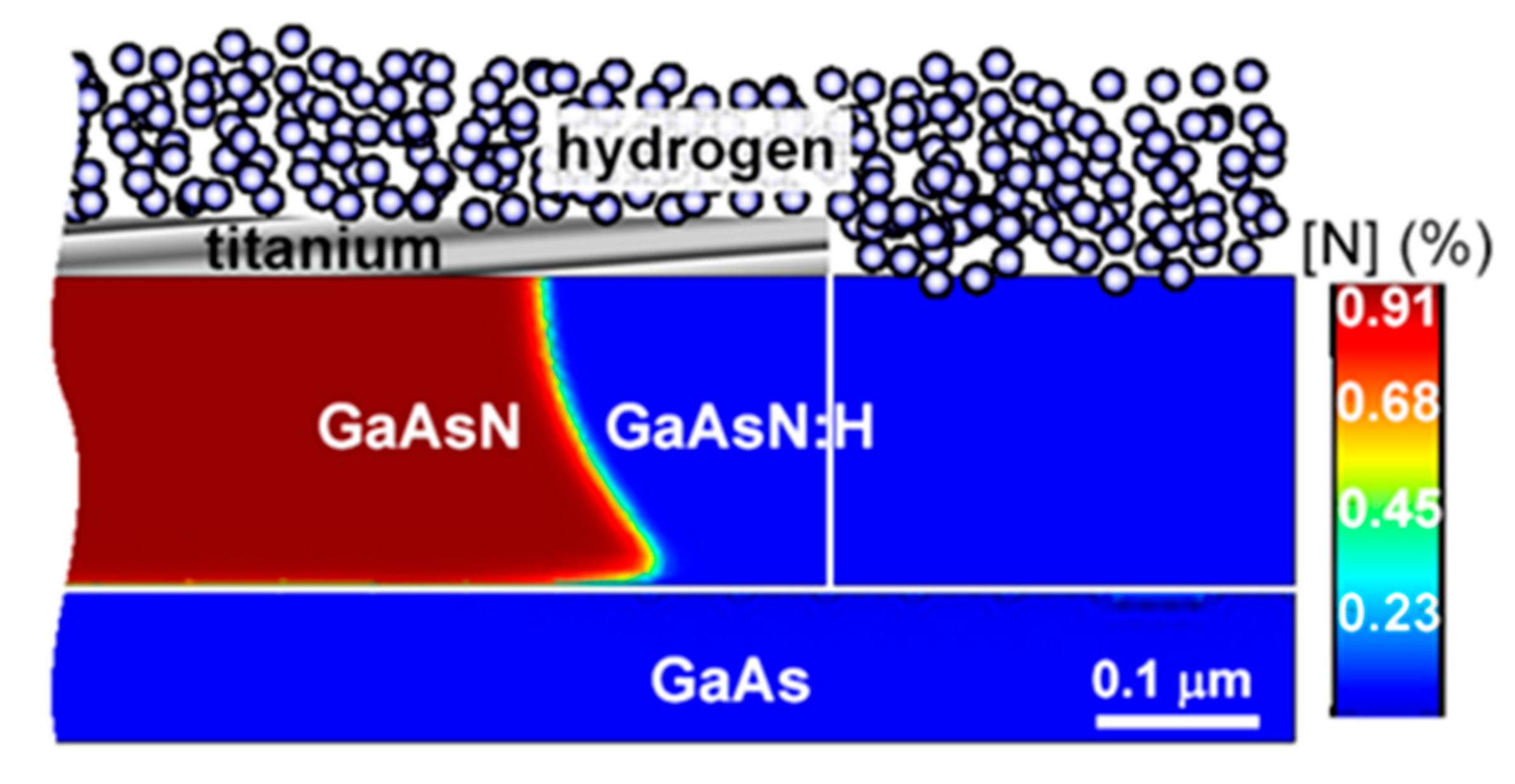
The combination of photoreflectance (PR) spectroscopy and micro-Raman scattering enabled us to perform an all-optical mapping of the strain field in GaAsN/GaAsN:H micro-wires. In fact, by means of PR and Raman scattering, the critical point energies near the energy gap (on a macroscopic scale) and the strain dependence of the longitudinal optical (LO) phonon frequency ωLO (on a microscopic scale) can be measured [23,24,25,26,27], respectively. As shown in the following, the combined peculiarities of the two experimental approaches allowed to obtain a detailed picture of the strain field resulting from H distribution across the wires. Moreover, the strain field mapping was found to qualitatively agree with simulations based on a system of partial differential equations that reproduce the kinetics of hydrogen in GaAsN [28].

2.2. Samples

As reported in Ref. [16], the samples used to test the strain field mapping were made by growing a GaAs0.991N0.009 film on a GaAs buffer. The film was grown by molecular beam epitaxy at 500 °C. Thickness was 200 nm. The buffer was deposited on a [001] GaAs substrate at 600 °C. A radio-frequency plasma source was employed for N2 cracking. X-ray diffraction measurements allowed the characterization of the film regarding thickness and nitrogen concentration. The GaAsN surface was covered with a 50 nm thick film of titanium, which is not transparent to hydrogen. Electron beam lithography was used to pattern the Ti film. A 100 eV ion beam produced hydrogenation with a H dose ≈ 3 × 10¹⁸ ions/cm2. Such dosage allows the full passivation of an unpatterned GaAsN layer of the same thickness. Finally, chemical etching produced the removal of the titanium masks. It must be noted that a sharp GaAsN/GaAsN:H interface can be accomplished between GaAsN wires and the hydrogenated barriers [29], now exhibiting a “GaAs-like” behavior. In fact, hydrogen diffuses In GaAsN with a steep front-line of 10 nm/decade, or less [30].
The hydrogenation process that was used to create the vertical GaAsN/GaAsN:H interfaces defining the wires is illustrated in Figure 1. The figure shows the concentration of electronically active nitrogen atoms following hydrogenation when a 10 µm wide titanium mask is used. In the examined sample of composition GaAs0.991N0.009, wires of different width w (w = 0.5, 1, 2, 5, and 10 µm) and parallel to the [110] (or equivalent) direction were interposed with hydrogenated barriers (10–20 µm wide).

2.3. PR Measurements and Average Strain Determination

Near-normal incidence PR measurements were collected in the energy range of interest (here typically 1.1–1.9 eV) with a spectral resolution of 1 meV. The probe beam of the standard experimental apparatus [31] was obtained from a 100 W halogen lamp, while the modulated excitation source was provided by the continuous output of a 20 mW Coherent HeNe laser (λ = 632.8 nm; 1-mm spot diameter) mechanically chopped at a frequency of 220 Hz.
Typical PR spectra, obtained at room-temperature in the energy range of interest, are shown in Figure 2 for the multi-wires sample (panel a) and for the as-grown GaAsN reference sample (panel b). Despite the presence of the articulated and bulky spectral structures (near 1.42 eV), due to signals coming from the buffer/substrate region and related to the GaAs band gap [27], some PR features particularly interesting for determining the strain status of the GaAsN layer can be observed in both spectra.
More in depth:
(i)
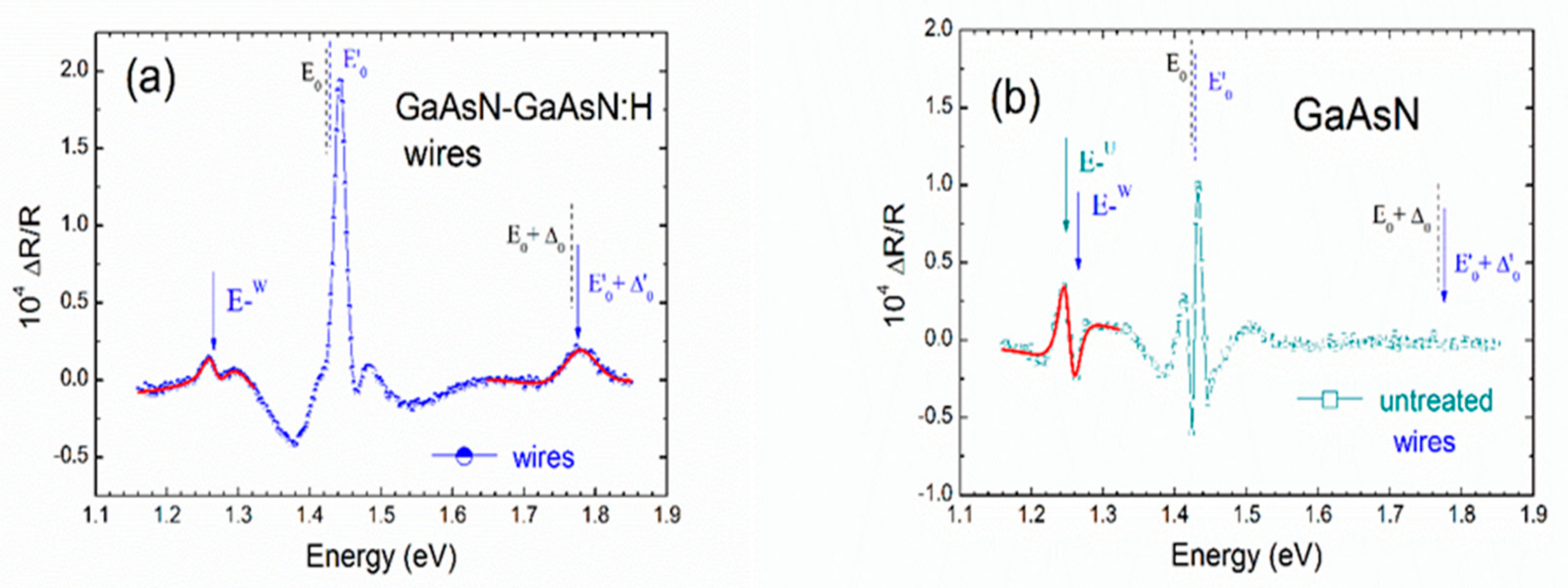
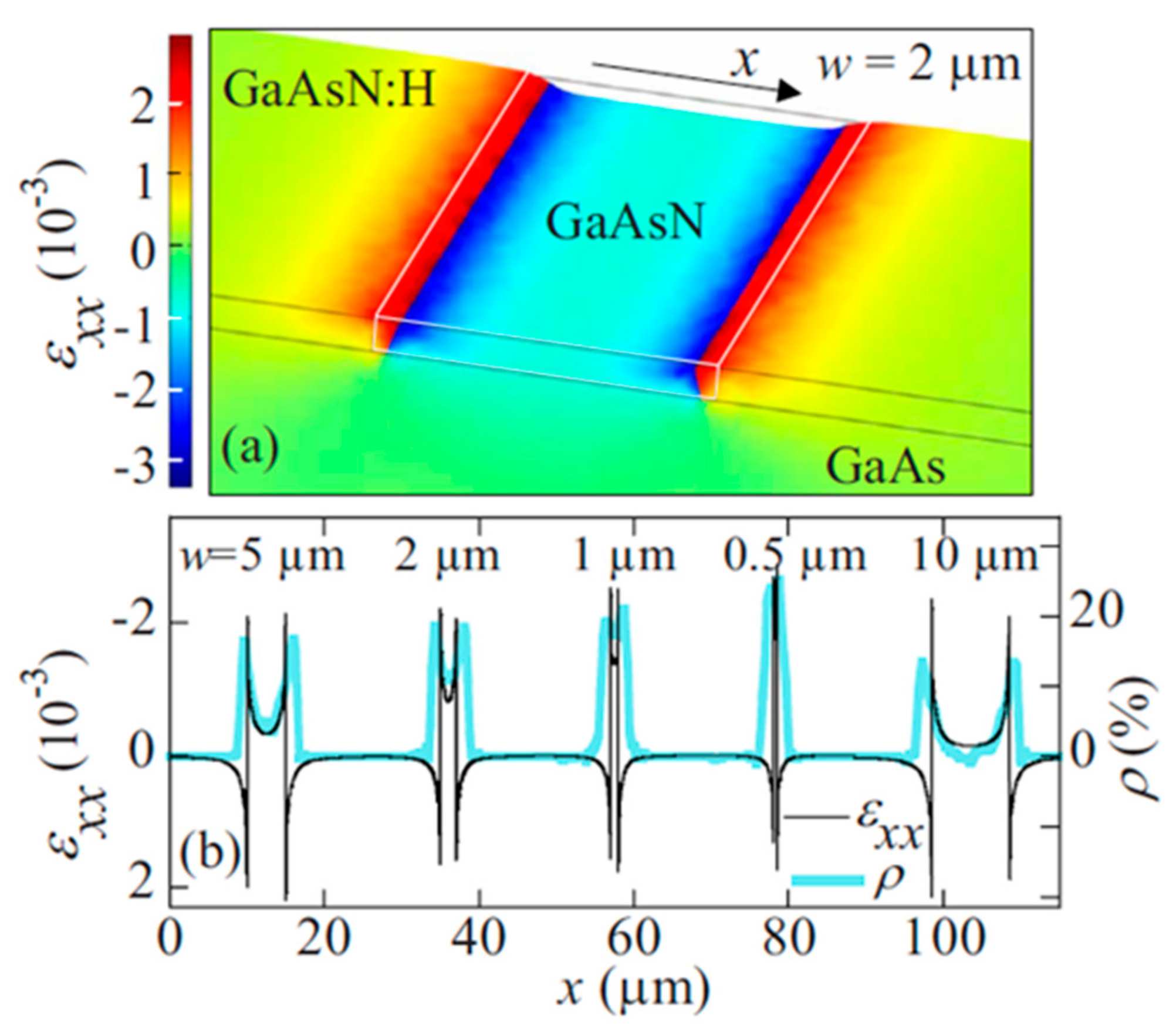
In the multi-wires sample (Figure 1, panel a), the “GaAs-like” spectral structures of the band gap (E0) and of the split-off (SO) band (E0 + ∆0) are due to the optical response of the surface barriers between the GaAsN wires, that hydrogenation has turned into “GaAs-like” sections [9,10,11]. As previously observed [8,10,32], the broadening parameters of these features appear greatly enhanced and their energy position is systematically blueshifted with respect to the corresponding features, E0 and E0 + ∆0, that can be found in the literature of GaAs materials. In particular, the SO blueshift of (9 ± 1) meV [16], obtained by fitting the spectral structure to the appropriate Aspnes line-shape model function [27], must be related to a sizeable expansion of the host lattice resulting from hydrogenation [10,11] and can be used to determine the in-plane strain. An analytical procedure based on the deformation potential theory [25], and thoroughly described elsewhere [10], leads to a value of the average compressive in-plane strain ε// (in the hydrogenated sections) roughly equal to −1.0 × 10⁻³.
(ii)
In the low energy part of the same spectrum (Figure 1, panel a) one can see the contribution to the PR signal coming from the GaAsN sections (wires). It originates from the presence of the E-band [6,7] at E-w = 1.265 eV, as determined by a best fit. This value is 11 meV higher than that (E-u = 1.254 eV) obtained for the same band in the untreated GaAsN sample (see Figure 2, panel b). One should note that the strain field produces shift and splitting of GaAsN valence bands [6,7]. On the other hand, at room temperature, probably due to broadening effects, the doublet is unresolved in the optical response of both samples. For this reason, a single Aspnes model function [27] was used to derive the energy (E-) of the band gap of GaAsN. According to the deformation potential theory [23], the energy gap increases for decreasing tensile stress, and indeed, this is our case. Therefore, the tensile strain in the previously masked wire sections of the hydrogenated multi-wires sample (see Figure 2) is expected to largely decrease, in good agreement with the observation of a compressive strain produced on GaAsN wires by a lattice expansion in the hydrogenated barriers [11].
(iii)
After lowering the temperature of the sample, the improved experimental conditions allowed the doublet in the E- band of the spectra of the untreated GaAsN sample to be resolved (not shown) and to measure a valence band splitting ∆E = (14 ± 2) meV, that corresponds [10,30] to an in-plane tensile strain ε// ≈ + 1.8 × 10⁻³. It must be pointed out that this value is very close to that expected for the coherent growth of a GaAs0.991N0.009 layer on GaAs. We note that, due to the increased broadening parameters, the same procedure could not be applied in the case of the multi-wires sample.

2.4. Raman Scattering Measurements and Micro-Scale Mapping of the Strain Field

All the Raman spectra reported in this paper were obtained using micro-Raman equipment. The light source was a HeNe laser (λ = 632.8 nm). Spectral resolution was 1 cm−1. As reported in Ref. [16], the average in-plane strain can be nicely reproduced by the frequency variation of the longitudinal optical mode (ωLO) with respect to the unstrained material. The compressive/tensile nature of the strain is marked by increasing/decreasing frequencies, even on a microscopic scale [33,34,35,36,37].
In Figure 3, spectra recorded at the axis of a GaAsN wire (of width w = 10 μm), and in the hydrogenated barrier far from the wire, are reported. One can appreciate how the Ga-N line at 475 cm−1, typical of the untreated alloy, disappears after hydrogenation. The GaAs-like LO and transverse optical (TO) phonons produce a relatively intense line at about 292 cm−1 and a rather weak line at about 270 cm−1, respectively. The LO phonon frequency shifts to higher values in the hydrogenated barrier, in agreement with [8]. This is clearly shown in Figure 4a, whereas Figure 4b evidences the composition profile across the wire resulting from the intensity profile of the Ga-N local mode. Panel 4b reveals that the wire-barrier interface is sharp, actually not resolved as the diffraction-limited laser spot diameter is about 0.7 µm. In contrast, the LO frequency profile reveals that frequency variation at the interface is not steep, but extends over a few microns, which can be neatly resolved by the Raman probe. This can be attributed to uniaxial stress (and strain) extending far beyond the interface thickness.

2.5. Data Reduction

We devised a data reduction method which allows to isolate the LO mode frequency shift produced by strain components other than the biaxial strain [38] associated with the lattice parameter mismatch between the GaAs buffer and the pseudomorphic materials GaAsN and GaAsN:H in the planar heterostructure. To this aim, we assume a linear relation between the isotropic biaxial in-plane strain and the LO phonon frequency. Near the wire-barrier interfaces we also assume a linear relation between the anisotropic components of the strain and the phonon frequency.
These local strain components, in turn, are linearly related to Xxx, the diagonal component of the stress acting perpendicularly to the wire/barrier interfaces. It follows that a linear relationship holds between the phonon frequency and the Xxx stress component. Figure 4, panel (c) illustrates the data reduction method. Inside the wire, the LO phonon frequency data have been incremented by +1.0 cm−1. This amount corresponds to double the shift between the LO frequency in the hydrogenated barrier far from the interface and at the interface. The procedure follows from two assumptions: (i) The elastic constants are equal in the untreated and in the hydrogenated GaAs0.991N0.009 alloy, and (ii) they are in accordance with symmetry considerations in the proximity of the interface local uniaxial stress in the wire and in the barrier with equal intensity and the opposite sign. Finite element method (FEM) simulations [11] were made using the same parameters of the sample under experimental investigation. It turns out that the reduced data from Raman experiments favorably compare with the results of simulations, i.e., the uniaxial strain component εxx (linearly related to the diagonal Xxx stress component) in wires and barriers oriented in the [110] direction (see Figure 5). Both experiments and simulations, in particular, suggest that nonzero uniaxial stress exists even at wire axis, in accordance with the lack of a frequency plateau within the wire.

3. Raman Line Shape in Dilute Nitrides: Recent Evolution

The effects of the H dose on LO phonon frequencies have been recently investigated in uniformly hydrogenated layers of a GaAsN alloy with N concentration equal to 1% [39]. Measurements were made on samples which received H doses comprised between 1.2 and 3.5 c (1 c = 1.0 × 10¹⁸ ions/cm2), corresponding to the average in-plain biaxial strain ranging from 1.0 × 10⁻³ to −8.0 × 10⁻³, as estimated from PR spectra [39]. The frequency evolution with an increasing H dose strongly depends on the polarization geometry of the Raman scattering experiment Table 1.
While in the typically used geometry (incident and scattered light polarization [110]) the linear relationship between strain and frequency is confirmed [39] as supported by the comparison with the PR data for increasing doses (and increasing strain), in other geometries the behavior might be different. The most intriguing case corresponds to incident light polarization along the [100] crystallographic axis and scattered light polarization along the same [100] axis. In this geometry, Raman scattering is forbidden in GaAs, whereas selection rules are known to relax in strained GaAsN [40]. In-plane strain is also the main parameter responsible of the relaxation of selection rules in in GaAsN:H layers. The low scattering intensity in the 1.2 c sample [39] is amenable to the vanishing strain in this particular sample. Scattering intensities in more heavily irradiated samples are larger, in agreement with a larger (compressive) strain, as confirmed by systematic PR measurements [30,39]. In contrast to other geometries, frequencies decrease with an increasing H dose, which is accompanied by an increasing compressive strain. In all micro-Raman experiments on H-irradiated samples, laser power must not exceed the threshold above which dissociation of N-H centers starts to occur [41]. With the instrumental setup typically used in our experiments, such threshold can be prudently set at 1 mW [16]. However, a marked dependence of line shapes (peak position, broadening, symmetry) on power was observed (see Figure 6) starting from about 0.3 mW, especially in more heavily hydrogenated GaAsN samples. It is worth noting that the data reported in Table 1 for GaAsN:H layers were obtained by using an excitation power of 0.1 mW. No comparable effect is observed in GaAs, while it was found negligible in GaAs1−xNx (at least for x ≤ 0.01). This effect is completely reversible, so that it is reasonable to believe that it cannot be ascribed to N-nH center dissociation [41,42]. Although further investigation (actually in progress) will be required to fully explain these results, we may notice that the temperature increase due to the laser beam illumination could enhance the free carriers (originating from ionized impurities) activity and locally modify the pre-existing charge density distribution around the N-nH complexes, so adding disorder in the host matrix [20,43]. Since the power effect is completely reversible, we may infer that although the temperature increase is not enough for hydrogen evaporation [20,43,44], nevertheless it favors the introduction of further disorder in the host matrix. This is consistent with the experimentally observed dependence of the redshift of the peak frequency of the Raman LO GaAs-like mode on the power of the laser beam. In fact, the deformation of the line shape of the Raman structures, in particular redshift of the peak frequency, broadening increase and asymmetry of the shape may be accounted for (at least partially) by the laser-beam-induced temporary increase of the lattice disorder. This last is known to produce many of the aforementioned effects on the Raman line shapes in III–V semiconductors [45,46]. Whatever the precise explanation of this “power effect”, it is clear that one must operate very carefully with hydrogenated GaAsN materials and heterostructures to avoid spectral line distortion.

4. Conclusions

In the past few years, Raman scattering has been successfully used to investigate the strain state of GaAsN and GaAsN:H layers. The technique is based on the dependence of GaAs-like phonon frequencies on strain through the phonon deformation potentials. Raman scattering microscopic results compare well with the average in-plane strain determination, independently obtained via PR measurements on a macroscopic scale. In particular, it was possible to relate the GaAs-like LO phonon frequency shift to the H dose received by the sample, hence to the amount of in-plane strain. Checking this linear relation takes advantage of the PR well-established compressive strain dependence on H dose. Remarkably, micro-Raman mapping allowed to gain detailed information about the strain distribution in GaAsN/GaAsN:H heterostructures. A Raman shift in heterostructures depends on both biaxial in-plane strain and uniaxial strain components acting at the interface between, e.g., GaAsN wires and GaAsN:H matrix. It is possible, at least in simple cases, to isolate the strain components other than the biaxial strain. The result of such data reduction is in qualitative agreement with finite element method simulations. The techniques described here can help design devices based on the strain engineering of GaAsN/GaAsN:H heterostructures. Work is in progress concerning wire-barrier heterostructures with different orientations with respect to the crystallographic axes.

Funding

This research received no external funding.

Conflicts of Interest

The authors declare no conflict of interest.

References

  1. Anastassakis, E.; Burstein, E. Morphic effects II-effects of external forces on the frequencies of the q ≈ 0 optical phonons. J. Phys. Chem. Solids 1971, 32, 563–570. [Google Scholar] [CrossRef]
  2. Anastassakis, E.; Pinczuk, A.; Burstein, E.; Pollak, F.H.; Cardona, M. Effect of static uniaxial stress on the Raman spectrum of silicon. Solid State Commun. 1970, 8, 133–138. [Google Scholar] [CrossRef]
  3. Anastassakis, E. Angular dispersion of optical phonon frequencies in strained cubic crystals. J. Appl. Phys. 1997, 81, 3046–3056. [Google Scholar] [CrossRef]
  4. Sood, A.K.; Anastassakis, E.; Cardona, M. Raman piezospectroscopy in GaAs revisited. Phys. Status. Solidi. (b) 1985, 129, 505–512. [Google Scholar] [CrossRef]
  5. Bazzan, M.; Kokanyan, N.; Zaltron, A.; Argiolas, N.; Chapron, D.; Fontana, M.D. Raman frequency shift induced by photorefractive effect on Fe-doped lithium niobate. J. Appl. Phys. 2013, 114, 163506. [Google Scholar] [CrossRef]
  6. Henini, M. Dilute Nitride Semiconductors: Physics and Technology; Elsevier: Oxford, UK, 2005. [Google Scholar]
  7. Buyanova, I.A.; Chen, W.M. Physics and Applications of Dilute Nitrides; Taylor & Francis Books Inc.: New York, NY, USA, 2004. [Google Scholar]
  8. Klar, P.J.; Gruning, H.; Gungerich, M.; Heimbrodt, W.; Koch, J.; Torunski, T.; Stolz, W.; Polimeni, A.; Capizzi, M. Global change of the band structure and the crystal lattice of Ga(N,As) due to hydrogenation. Phys. Rev. B 2003, 67, 121206. [Google Scholar] [CrossRef]
  9. Bisognin, G.; De Salvador, D.; Drigo, A.V.; Napolitani, E.; Sambo, A.; Berti, M.; Polimeni, A.; Felici, M.; Capizzi, M.; Grungerich, M.; et al. Hydronen-nitrogen complexes in dilute nitride alloys: Origin of the compressive lattice strain. Appl. Phys. Lett. 2006, 89, 061904. [Google Scholar] [CrossRef]
  10. Geddo, M.; Ciabattoni, T.; Guizzetti, G.; Galli, M.; Patrini, M.; Polimeni, A.; Trotta, R.; Capizzi, M.; Bais, G.; Piccini, M.; et al. Photoreflectance and reflectance investigation of deuterium-irradiated GaAsN. Appl. Phys. Lett. 2007, 90, 091907. [Google Scholar] [CrossRef]
  11. Trotta, R.; Polimeni, A.; Capizzi, M.; Martelli, F.; Rubini, S.; Francardi, M.; Gerardino, A.; Mariucci, L. Light polarization control in strain- engineered GaAsN/GaAsN:H heterostructures. Appl. Phys. Lett. 2009, 94, 261905. [Google Scholar] [CrossRef]
  12. Trotta, R.; Polimeni, A.; Capizzi, M. Hydrogen incorporation in III-N-V Semiconductors: From Macroscopic to Nanometer Control of the Materials’ Physical Properties. Adv. Funct. Mater. 2012, 22, 1782–1801. [Google Scholar] [CrossRef]
  13. Pettinari, G.; Felici, M.; Trotta, R.; Capizzi, M.; Polimeni, A. Hydrogen effect in dilute III-N-V alloys: From defect engineering to nanostructuring. J. Appl. Phys. 2014, 115, 012011. [Google Scholar] [CrossRef]
  14. Ciatto, G. Hydrogenated Dilute Nitride Semiconductors; Pan Stanford Publishing: Singapore, 2015. [Google Scholar]
  15. Geddo, M.; Pezzuto, R.; Capizzi, M.; Polimeni, A.; Gollub, D.; Fischer, M.; Forchel, A. Photoreflectance investigation of hydrogenated (InGa)(AsN)/GaAs heterostructures. Eur. Phys. J. B 2002, 30, 39–43. [Google Scholar] [CrossRef]
  16. Geddo, M.; Giulotto, E.; Grandi, M.S.; Patrini, M.; Trotta, R.; Polimeni, A.; Capizzi, M.; Martelli, F.; Rubini, S. An all optical mapping of the strain field in GaAsN/GaAsN:H wires. Appl. Phys. Lett. 2012, 101, 191908. [Google Scholar] [CrossRef]
  17. Felici, M.; Pettinari, G.; Biccari, F.; Capizzi, M.; Polimeni, A. Spatially selective hydrogen irradiation of dilute nitride semiconductors: A brief review. Semicond. Sci. Technol. 2018, 33, 053001. [Google Scholar] [CrossRef]
  18. Felici, M.; Birindelli, S.; Trotta, R.; Francardi, M.; Gerardino, A.; Notargiacomo, A.; Rubini, S.; Martelli, F.; Capizzi, M.; Polimeni, A. Nanoscale tailoring of the polarization properties of dilute-nitride semiconductors via h-assisted strain engineering. Phys. Rev. Appl. 2014, 2, 064007. [Google Scholar] [CrossRef]
  19. Polimeni, A.; Bissiri, H.M.; Capizzi, M.; Fischer, M.; Reinhardt, M.; Forchel, A. Effect of hydrogen on the electronic properties of InxGa1−xAs1−yNy/GaAs quantum wells. Phys. Rev. B 2001, 63, 201304. [Google Scholar] [CrossRef]
  20. Berti, M.; Bisognin, G.; De Salvador, D.; Napolitani, E.; Vangelista, S.; Polimeni, A.; Capizzi, M.; Boscherini, F.; Ciatto, G.; Rubini, S.; et al. Formation and dissolution of D-N complexes in dilute nitrides. Phys. Rev. B 2007, 76, 205323. [Google Scholar] [CrossRef]
  21. Wen, L.; Stavola, M.; Fowler, W.B.; Trotta, R.; Polimeni, A.; Capizzi, M.; Bisognin, G.; Berti, M.; Rubini, S.; Martelli, F. Microscopic origin of compressive strain in hydrogen-irradiated dilute GaAs1−y Ny alloys: Role of N-Hn centers with n>2 and their thermal stability. Phys. Rev. B 2012, 86, 085206. [Google Scholar] [CrossRef]
  22. Bhattacharya, P. Semiconductor Electronic Devices; Prentice Hall: Englewood Cliffs, NJ, USA, 1997. [Google Scholar]
  23. Pollak, F.H. Effects of homogeneous strain on the electronic and vibrational level in semiconductors. In Semiconductors and Semimetals; Pearsall, T.B., Ed.; Academic: Boston, MA, USA, 1990; Volume 32, pp. 17–57. [Google Scholar]
  24. Pollak, F.H.; Cardona, M. Piezo-Electroreflectance in Ge, GaAs, and Si. Phys. Rev. 1968, 172, 816–837. [Google Scholar] [CrossRef]
  25. Geddo, M.; Guizzetti, G.; Patrini, M.; Ciabattoni, T.; Serravalli, L.; Frigeri, P.; Franchi, S. Metamorphic buffers and optical measurements of residual strain. Appl. Phys. Lett. 2005, 87, 263120. [Google Scholar] [CrossRef]
  26. Aspnes, D.E. Third-derivative modulation spectroscopy with low-field electroreflectance. Surf. Sci. 1973, 37, 418–442. [Google Scholar] [CrossRef]
  27. Aspnes, D.E.; Studna, A.A. Schottky-barrier electroreflectance: Application to GaAs. Phys. Rev. B 1974, 10, 4228–4238. [Google Scholar] [CrossRef]
  28. Trotta, R.; Giubertoni, D.; Polimeni, A.; Bersani, M.; Capizzi, M.; Martelli, F.; Rubini, S.; Bisognin, G.; Berti, M. Hydrogen diffusion in GaAs1−xNx. Phys. Rev. B 2009, 80, 195206. [Google Scholar] [CrossRef]
  29. Felisari, L.; Grillo, V.; Martelli, F.; Trotta, R.; Polimeni, A.; Capizzi, M.; Jabeen, F.; Mariucci, L. In-plane band gap modulation investigated by secondary electron imaging of GaAsN/GaAsN:H heterostructures. Appl. Phys. Lett. 2008, 93, 102116. [Google Scholar] [CrossRef]
  30. Trotta, R.; Polimeni, A.; Capizzi, M.; Giubertoni, D.; Bersani, M.; Bisognin, G.; Berti, M.; Rubini, S.; Martelli, F.; Mariucci, L.; et al. Effect of hydrogen incorporation temperature in in plane-engineered GaAsN∕GaAsN:H heterostructures. Appl. Phys. Lett. 2008, 92, 221901. [Google Scholar] [CrossRef]
  31. Geddo, M.; Guizzetti, G.; Capizzi, M.; Polimeni, A.; Gollub, D.; Forchel, A. Photoreflectance evidence of N-induced increase of the exciton binding energy in an In x Ga 1−x As 1−y N y alloy. Appl. Phys. Lett. 2003, 83, 470–472. [Google Scholar] [CrossRef]
  32. Geddo, M.; Patrini, M.; Guizzetti, G.; Galli, M.; Trotta, R.; Polimeni, A.; Capizzi, M.; Martelli, F.; Rubini, S. Optical study of hydrogen-irradiated GaAsN/GaAs heterostructures. J. Appl. Phys. 2011, 109, 123511. [Google Scholar] [CrossRef]
  33. Inoki, C.K.; Lemos, V.; Cerdeira, F.; Vasquez-Lopez, C. Strain determination in InxGaAs1-x/GaAs strained-layer superlattices by photomodulatd reflectance. J. Appl. Phys. 1993, 73, 3266–3270. [Google Scholar] [CrossRef]
  34. Shin, H.K.; Lockwood, D.J.; Lacelle, C.; Poole, P.J. Phonons in strained In1-xGaxAs/InP epilayers. J. Appl. Phys. 2000, 88, 6423–6428. [Google Scholar] [CrossRef]
  35. Jusserand, B.; Cardona, M. Light Scattering in Solids V. In Topics in Applied Physics; Cardona, M., Guntherodt, G., Eds.; Springer: New York, NY, USA, 1989; Volume 66, pp. 49–152. [Google Scholar]
  36. Cerdeira, F.; Buchnauer, C.J.; Pollak, F.H.; Cardona, M. Stress-induced shifts of first-order Raman frequencies of diamond- and zinc-blende-type semiconductors. Phys. Rev. B 1972, 88, 580–593. [Google Scholar] [CrossRef]
  37. Bellani, V.; Bocchi, C.; Ciabattoni, T.; Franchi, S.; Frigeri, P.; Galinetto, P.; Geddo, M.; Germini, F.; Guizzetti, G.; Nasi, L.; et al. Residual strain measurements in InGaAs metamorphic buffer layers on GaAs. Eur. Phys. J. B 2007, 56, 217–222. [Google Scholar] [CrossRef]
  38. Giulotto, E.; Geddo, M.; Patrini, M.; Guizzetti, G.; Felici, M.; Capizzi, M.; Polimeni, A.; Martelli, F.; Rubini, S. H irradiation effects on the GaAs-like Raman modes in GaAs1-xNx/GaAs1-xNx:H planar heterostructures. J. Appl. Phys. 2014, 116, 245304. [Google Scholar] [CrossRef]
  39. Giulotto, E.; Geddo, M.; Patrini, M.; Guizzetti, G.; Sharma, M.S.; Capizzi, M.; Polimeni, A.; Pettinari, G.; Rubini, S.; Felici, M. Strain related relaxation of the GaAs-like Raman mode selection rules in hydrogenated GaAs1−xNx layers. J. Appl. Phys. 2019, 125, 175701. [Google Scholar] [CrossRef]
  40. Mintairov, A.M.; Blagnov, P.A.; Melehin, V.G.; Faleev, N.N.; Merz, J.L.; Qiu, Y.; Nikishin, S.A.; Temkin, H. Ordering effects in Raman spectra of coherently strained GaAs1-xNx. Phys. Rev. B 1997, 56, 15836–15841. [Google Scholar] [CrossRef]
  41. Balakrishnan, N.; Patanè, A.; Makarovsky, O.; Polimeni, A.; Capizzi, M.; Martelli, F.; Rubini, S. Laser writing of the electronic activity of N- and H-athoms in GaAs. Appl. Phys. Lett. 2011, 99, 021105. [Google Scholar] [CrossRef]
  42. Ciatto, G.; Pettinari, G.; Balakrishnan, N.; Berenguer, F.; Patanè, A.; Birindelli, S.; Felici, M.; Polimeni, A. Synchrotron x-ray diffraction study of micro-patterns obtained by spatially selective hydrogenation of GaAsN. Appl. Phys. Lett. 2015, 106, 051905. [Google Scholar] [CrossRef]
  43. Du, M.; Limpijumnong, S.; Zhang, S. Hydrogen pairs and local vibrational frequencies in H-irradiated GaAs1−yNy. Phys. Rev. B 2005, 72, 073202. [Google Scholar] [CrossRef]
  44. Bisognin, G.; De Salvador, D.; Napolitani, E.; Berti, M.; Polimeni, A.; Capizzi, M.; Rubini, S.; Martelli, F.; Franciosi, A. High-resolution x-ray diffraction in situ study of very small complexes: The case of hydrogenated dilute nitrides. J. Appl. Crystallogr. 2008, 41, 366–372. [Google Scholar] [CrossRef]
  45. Parayanthal, P.; Pollak, F.H. Raman Scattering in Alloy Semiconductors: “Spatial Correlation” Model. Phys. Rev. Lett. 1984, 52, 1822–1825. [Google Scholar] [CrossRef]
  46. Liu, H.F.; Xiang, N. Raman scattering probe of anharmonic effects due to temperature and compositional disorder in GaNxAs1−x. J. Appl. Phys. 2006, 99, 103503. [Google Scholar] [CrossRef]
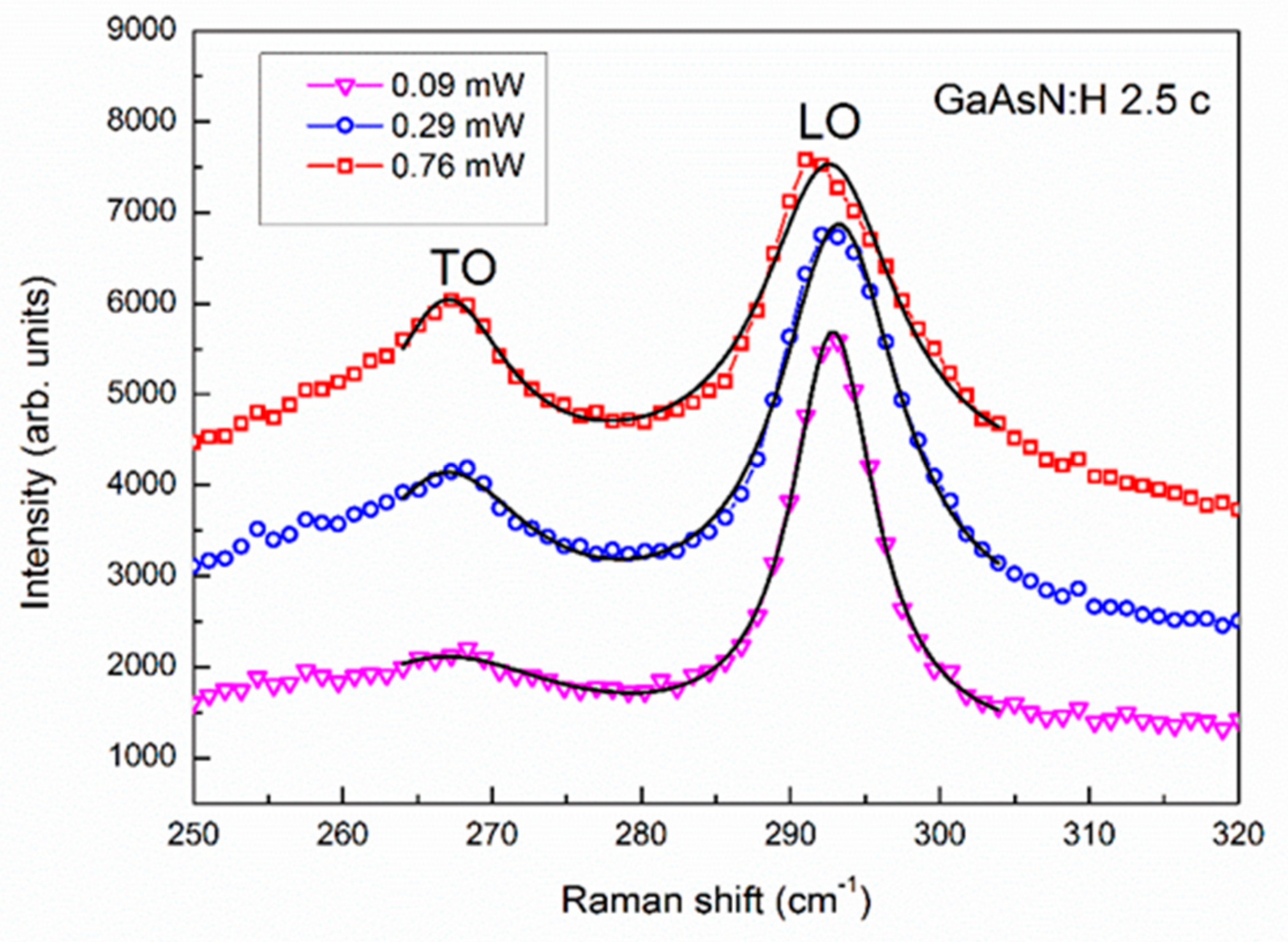
Figure 1. Schematic illustration of the hydrogenation process used to fabricate the GaAsN wires. View of a sample section near a GaAsN/GaAsN:H vertical interface (the actual wire is 10 µm wide). The wires run perpendicularly to the figure plane and the Ti wire is sketched as a greyish rectangle on the top surface. The color map shows the effective N concentration (namely, N atoms not passivated by H atoms), as derived quantitatively by extending in two dimensions and in the presence of a Ti mask, the model reported in Ref. [28]. The corresponding effective N concentration value is shown in a false color scale on the right. Reproduced from [16] (M. Geddo, E. Giulotto, M. S. Grandi, M. Patrini, R. Trotta, A. Polimeni, M. Capizzi, F. Martelli, and S. Rubini, Appl. Phys. Lett. 101, 191908 (2012). http://dx.doi.org/10.1063/1.4766285), with the permission of AIP Publishing.
Applsci 09 04864 g001
Figure 2. (a) Room-temperature PR spectra of the multi-wires sample; (b) the same for the untreated GaAsN reference sample. The PR features near 1.26 eV are typical of dilute nitrides and mark the redshifted GaAsN fundamental gap (E- band) both in the spectrum of the multi-wires sample (E-w) and in the one of the untreated GaAsN sample (E-u). In panel (a), note the blueshift of the SO transition energy E0 + Δ0 (due to PR signal coming from the hydrogenated sections of the multi-wires sample) with respect to the one of GaAs (E0 + Δ0). At the same time, also note that in the wire sections, the increased energy of the E- band (with respect to the untreated sample) highlights the reduced tensile character of their strain state. In both panels, arrows mark the transition energy, as obtained from the best fit (solid continuous lines) of the experimental line-shape. The transition energy of the GaAs fundamental gap E0 and SO band E0 + ∆0 (as obtained from literature data, see Ref. [27]) and of the GaAs0.991N0.009:H fundamental gap E0 (as obtained from simulation results) are also reported (dashed bars).
Applsci 09 04864 g002
Figure 3. (a) Room-temperature Raman spectrum taken at the center of a 10 μm wide GaAsN wire; (b) the same, taken in the hydrogenated barrier far from the wire axis. Note the vanishing of the LVM line in the fully hydrogenated part of the barrier. Reproduced from ([16] M. Geddo, E. Giulotto, M. S. Grandi, M. Patrini, R. Trotta, A. Polimeni, M. Capizzi, F. Martelli, and S. Rubini, Appl. Phys. Lett. 101, 191908 (2012). http://dx.doi.org/10.1063/1.4766285), with the permission of AIP Publishing.
Applsci 09 04864 g003
Figure 4. (a) GaAs-like LO phonon frequency along a direction perpendicular to 10−μm wide wire (see section “Experimental and analytical procedure”). In-plane strain values in the hydrogenated barriers and in the untreated GaAsN reference sample obtained by PR measurements are also reported as described in section “PR measurements and average strain determination”. (b) Ga-N mode Raman integrated intensity at the same positions of panel (a). (c) Full dots: Same data reported in panel (a) after the data reduction procedure described in section “Data reduction”. Shift with respect to the frequency measured in barriers far from interfaces is proportional to uniaxial stress Xxx (right axis scale). Empty dots: GaAs-like LO phonon frequency profile in the wire before data reduction. Dashed vertical lines indicate wire-barrier interfaces, as derived from data in panel (b). Reproduced from([16] (M. Geddo, E. Giulotto, M. S. Grandi, M. Patrini, R. Trotta, A. Polimeni, M. Capizzi, F. Martelli, and S. Rubini, Appl. Phys. Lett. 101, 191908 (2012). http://dx.doi.org/10.1063/1.4766285) and from ([38] E. Giulotto, M. Geddo, M. Patrini, G. Guizzetti, M. Felici, M. Capizzi, A. Polimeni, F. Martelli, and S. Rubini, J. Appl. Phys. 116, 245304 (2014). http://dx.doi.org/10.1063/1.4905097), with the permission of AIP Publishing.
Applsci 09 04864 g004
Figure 5. (a) Calculated 3D distribution of the uniaxial strain field component εxx, that is in the direction perpendicular to the axis of a 2.0-µm wide wire (see section “Experimental and analytical procedure”). Deformation is 100 times exaggerated. (b) Calculated εxx along the normal to the wire axis (black line), see Ref. [11]. Note the agreement with the experimental polarization degree ρ (thick blue line, right axis). Reproduced from [11] (R. Trotta, A. Polimeni, M. Capizzi, F. Martelli, S. Rubini, M. Francardi, A. Gerardino, and L. Mariucci, Appl. Phys. Lett. 94, 261905 (2009) https://doi.org/10.1063/1.3157838), with the permission of AIP Publishing.
Applsci 09 04864 g005
Figure 6. Room-temperature Raman spectra (incident and scattered light polarization [110]) taken using different laser power on a GaAsN:H sample (N concentration = 1%; H dose = 2.5 × 10¹⁸ ions/cm2). Note the GaAs-like LO mode peak intensity redshifts for increasing excitation power. Full lines represent fitting the data to a two-Lorentzian model accounting for LO and TO GaAs-like modes.
Applsci 09 04864 g006
Table 1. Frequencies of GaAs-like LO phonons obtained with different polarization geometries. Reproduced from [39] (E. Giulotto, M. Geddo, M. Patrini, G. Guizzetti, M.S. Sharma, M. Capizzi, A. Polimeni, G. Pettinari, S. Rubini, and M. Felici, J. Appl. Phys. 125, 175701 (2019) https://doi.org/10.1063/1.4905097), with the permission of AIP Publishing.
Incident Light PolarizationScattered Light PolarizationGaAs
Reference
GaAsN1.2c H Dose2.5c H Dose3.5c H Dose
[110][110] (allowed)292.4 cm−1291.6 cm−1292.5 cm−1292.8 cm−1293.2 cm−1
[110][1–10] (forbidden)-----
[100][010] (allowed)292.6 cm−1292.2 cm−1293.5 cm−1293.9 cm−1294.2 cm−1
[100][100] (forbidden)-290.4 cm−1290.1 cm−1289.6 cm−1289.8 cm−1

