Article

A Theoretical Study of the Energetic Stability and Geometry of Silicon-Vacancy Color Centers in Diamond (001) Surfaces

1
School of Power and Mechanical Engineering, Wuhan University, Wuhan 430072, China
2
Research Institute of Wuhan University in Shenzhen, Shenzhen 518057, China
3
Department of Quantum and Energy Materials, International Iberian Nanotechnology Laboratory, 4715-330 Braga, Portugal
*
Authors to whom correspondence should be addressed.
Appl. Sci. 2019, 9(24), 5471; https://doi.org/10.3390/app9245471
Submission received: 12 November 2019 / Revised: 26 November 2019 / Accepted: 10 December 2019 / Published: 12 December 2019
(This article belongs to the Section Applied Physics General)

Abstract

:
Single neutral silicon-vacancy ( SiV 0 ) color centers under H-, O-, or N-terminated diamond (001) surfaces were investigated using density functional theory. The formation energy calculation indicated that it is generally easier for SiV 0 to be embedded in an O-terminated diamond (001) surface as compared with H- and N-terminated surfaces, which were effected above the fifth C layer. The effects of the surface termination species on inner diamond atoms decay to be negligible below the fifth C layer. The binding energy results indicated that SiV centers exhibited rather high energetic stability once formed. Additionally, it was revealed that these three surface-terminating species had contracting or expanding effects on inner surface atoms. The calculation for density of states showed that the N-terminated diamond (001) surface served as a suitable medium for single SiV 0 to function as a single-photon source.

1. Introduction

Diamond is known for having excellent mechanical hardness, thermal conductivity, chemical inertness, and extraordinary optical properties [1,2]. In recent decades, research pertaining to the luminescent point defects (i.e., color centers) in diamond has attracted significant attention, owing to their promising application in quantum information processing [3,4,5], quantum sensing [6,7], and biological imaging [8,9].
Among the more than 500 types of color centers documented in diamond, only a small number have shown the potential for being bright and stable single-photon sources [10,11], including the most well-investigated, nitrogen-vacancy (NV) center [12,13], silicon-vacancy (SiV) [14,15] center, and the so-called NE8 [16,17], Cr-related [18] and germanium-vacancy (GeV) [19] centers. The photoluminescence (PL) spectra of the NV center in a neutral charge state ( NV 0 ) and the negatively charged nitrogen-vacancy ( NV ) center display a zero phonon line (ZPL) at 575 nm (2.156 eV) and 637 nm (1.945 eV), with a characteristic broad phonon sideband that extends from 580 to 650 nm and to 800 nm, respectively. As a result, only 4% of the emission of NV is concentrated in its ZPL, showing a Debye–Waller (DW) factor of 0.04. The primary unsatisfying aspects of NV centers as single-photon sources are their broad PL emission spectra and relatively long and variable fluorescence lifetime of up to ~24 ns [20,21,22] in nanodiamonds (NDs), which fail to meet the key requirements [10] for ideal single-photon sources. In contrast, negatively charged silicon-vacancy ( SiV ) centers exhibit a sharp ZPL at 738 nm (1.681 eV) at room temperature, with a large DW factor of 0.7 [23] and a short luminescence lifetime of 1 to 4 ns [24]. Similar to SiV , the SiV center in a neutral charge state ( SiV 0 ) also possesses a high DW factor (~0.9), with most of its emitted light concentrated into the ZPL at 946 nm (1.31 eV) [25], rendering SiV 0 a promising candidate for serving as single-photon emitters.
The SiV 0 has a ground state electron spin of S = 1. Single SiV defects in diamond are composed of a silicon substituting a C atom (Si) and a vacancy (V) in the nearest neighboring C site. Unlike the NV center, where the nitrogen atom is covalently bonded to its three nearest C atoms, and thus exhibiting C 3 V structural symmetry, the SiV center theoretically forms a split-vacancy structure (i.e., a silicon atom located at a bond-center site) in bulk diamond (Figure 1), thus, exhibiting D 3 d symmetry.
To improve the integrability, sensitivity, and spatial resolution of single-photon sources, they are generally produced into NDs, or as diamond thin films, in an attempt to embed them close to the diamond surface. To date, many reports have been published on the successful fabrication and characterization of SiV centers into NDs or in diamond thin films via the in situ method, i.e., doping during the chemical vapor deposition (CVD) synthesis processing of diamond [15,26,27,28,29,30], ion implantation [14,25,31] and femtosecond laser ablation [32]. However, to the best of our knowledge, the energetic stability and geometry of a single SiV center positioned in the vicinity of a diamond surface using different surface termination species remain poorly understood, despite theoretical and experimental studies on the effects of different surface states on the PL of SiV centers near a diamond surface [29,33].
The purpose of this study was to theoretically investigate the surface geometric structures and energetic stability of a single SiV 0 center positioned in the vicinity of diamond (001) surfaces (from the second to the seventh C layer, denoted as L2 to L7 in the following discussion), under fully H-, O- or N-terminated configurations. A diamond (001) surface was chosen, because at present, it is the most often employed and promising of diamond surfaces. Calculations were based on density functional theory (DFT) [34,35] methods under periodic boundary conditions.

2. Materials and Methods

All DFT calculations, in this study, were carried out using the Cambridge Sequential Total Energy Package [36]. More specifically, an ultrasoft pseudopotential [37] plane wave approach was adopted in the calculations, based on the Perdew–Burke–Ernzerhof generalized gradient approximation [38] for estimating the exchange-correlation functional. The energy cut-off for the plane wave basis sets was 400 eV, and a Monkhorst–Pack scheme [39] (which was used for k-point sampling of the Brillouin zone) of 2 × 2 × 1 k-points was used for structural optimization processes and self-consistent energy calculations of diamond slabs. For geometry optimization, the convergence tolerances for energy, maximum force, and maximum displacement were 1.0 × 10 5 eV/atom, 0.03 eV/Å, and 0.001 Å, respectively. The lattice constant of diamond was calculated as being 3.558 Å (where a 6 × 6 × 6 k-points mesh was used for an eight-atom primitive diamond lattice), which was in excellent agreement with the experimental value [40]. All parameters were selected following careful test calculations, ensuring the convergence of subsequent results.
The H-, O- and N-terminated diamond (001) surfaces were modeled as slabs with sizes of roughly 10.06   ×   10.06   ×   24.27   Å 3 and comprised 14 C layers with 224 C atoms in total when perfect, alongside a vacuum layer thickness of 11 Å. Here, the thick vacuum layer of 11 Å was large enough to ensure that the electric field decays were negligible within the vacuum, thus preventing artificial charge transfer between the two polar ends of the slab and its replica. Meanwhile, 14 layers of C, with the dangling bonds of the lowest layer of C atoms saturated with hydrogen atoms, were tested and found to be adequate for simulating bulk diamond. These H atoms were, together with the lowest layer of C atoms, fixed in space during the geometry optimization process and during subsequent calculations. The remaining atoms in the slabs were allowed to relax freely using the Broyden–Fletcher–Goldfarb–Shanno algorithm [41].
The formation energy E f [ X q ] of defect or impurity X in a charge state of q with respect to the perfect H-, O-, and N-terminated surface or bulk diamond, respectively, is defined as [42]
E f [ X q ]   =   E t o t d e f e c t [ X ,   q ]   E t o t p e r f e c t       n i μ i     q [ E F   +   E V + Δ V ] ,
where E t o t d e f e c t [ X ,   q ] is the total energy of the slab or bulk diamond containing defects in the supercell, E t o t p e r f e c t is the total energy of the perfect H-, O-, or N-terminated diamond (001) surface or bulk diamond, n i denotes the total number of atoms of element i (host atoms C or impurity silicon atoms (Si) removed from ( n i < 0 ) or added to ( n i > 0 ) in the diamond model), and μ i refers to the chemical potential of element i. The value of μ C is the energy of an individual C atom, obtained from the total energy of a perfect 216-atom diamond supercell, whereas μ S i was deduced from cubic silicon carbide (SiC). E F is the Fermi level with respect to the valence band maximum (VBM) ( E V ), and Δ V is the necessary correction for aligning the electrostatic potentials between the perfect surface and a surface with defects in a charged state. The final term is zero, because, in our work, we primarily investigated the E f of a diamond surface and of bulk diamond with defects in a neutral charge state. A negative value of formation energy corresponded to an easier formation process with lower energetic barriers.
The binding energy E b of a specific SiV is defined in terms of formation energies as follows: [42]
E b   =   E f [ S i ]   +   E f [ V ]     E f [ S i V ]
In which a positive binding energy indicates a stronger-bonded and more stable complex.
To further substantiate the validity of our calculation methods, we also calculated the formation energies of a single vacancy positioned in the first and second C layers in a bare diamond (001) surface as being 2.51 and 4.76 eV, respectively. These values matched well with those found in existing work (2.69 and 4.39 eV, respectively) [43]. In addition, the calculated adsorption energy per adsorbate species (as calculated in our previous work [2]) for a fully H-terminated diamond (001) surface was 5.37 eV, indicating a good agreement with reported results (5.36 eV [2] and 5.32 eV [44]). Furthermore, we calculated the adsorption energy per adsorbate species for a completely O-terminated diamond (001) surface as being 6.27 eV, which showed good agreement with existing work (6.20 eV [2] and 6.21 eV [45]).

3. Results and Discussion

SiV color centers near diamond surfaces are generally fabricated using in situ doping during the CVD process, ion implantation, or femtosecond laser ablation, as previously noted. These three approaches involve the formation of substitutional Si impurities and vacancies, and SiV is formed via the combination of Si and V. Therefore, prior to the investigation of single SiV, it is necessary to carefully consider the energetic stability and geometric structures of single Si and V, respectively.

3.1. Single Substitutional Silicon Impurity in H-, O-, and N-Terminated C (001) Surfaces

Single substitutional silicon (Si) impurity in a diamond (001) surface was modeled by replacing one C atom with a silicon atom near the surface. According to the analysis of the symmetry of surface structures, two different possible silicon-substituting positions were considered in the third, fourth, and seventh C layers of the H-terminated surface; and in the second, third, sixth, and seventh C layers of the N-terminated surface: under dimeric rows (Lm-1, where m refers to the C layer number) and between rows (Lm-2). For the O-terminated surface, there was only one possible site in every single C layer. The possible silicon-substituting positions (in L2 to L7) under H, O, and N terminations are shown in Figure 2. The structures chosen here were used in our existing work [2,46], as they were the most normal and stable configurations among fully H-, O-, and N-terminated diamond (001) surfaces.
The formation energy E f of single Si positioned in various C layers of H-, O-, or N-terminated diamond (001) surfaces and in a 216-atom bulk diamond, calculated using Equation (1), is illustrated in Figure 3. The formation energies of Si substituting one C atom under the dimer rows (configuration 1) and between (configuration 2) conform to Figure 2.
As indicated in Figure 3, none of these configurations showed a negative formation energy value, which implied the presence of energy barriers against their formation from the perfectly terminated diamond (001) surface. However, we can see that the structure of Si replacing the C atom in the second C layer at configuration 2 under N termination led to the smallest formation energy of 2.64 eV. Si replacing the L2 and the L3-2 C sites under H termination also showed similar small formation energies of 2.70 eV. For all possible configurations under O termination, large formation energies of more than 4.5 eV were found, which meant, as compared with H and N terminations, that an O-terminated diamond (001) surface introduced the effect of preventing the formation of silicon impurity.
Regarding the drastic difference between the formation energies of single Si in configuration 1 and 2 within the first four C layers under H and N terminations, this potentially occurred because of the local structural and electronic environments near the surface being significantly different between configurations 1 and 2. As shown in Table 1, bond lengths around configuration 2 in the first four C layers were much longer than those in configuration 1 under H and N terminations. However, for the O-terminated surface, there was only one possible Si-doping site in each C layer because of its high symmetry, and as indicated in Table 1, its bond lengths were almost the same below the second C layer; and thus its formation energies for single Si, positioned in various C layers, were similar when below the second C layer, as shown in Figure 3.
Additionally, for silicon impurities positioned deeper than the fifth C layer (including the fifth layer) from the surface, their formation energies were close to 4.7 eV, regardless of their termination state, which indicated that surface effects decayed to nearly negligible levels below the fifth C layer under diamond (001) surfaces. This conclusion was confirmed in Table 1, where the bond lengths between C atoms below the fifth C layer under H, O, or N termination were nearly constant at roughly 1.54 Å, which was the calculated C–C bond length value in the 216-atom bulk diamond. This value was in excellent agreement with the well-accepted value of 1.544 Å [47]. Meanwhile, the formation energies of single Si in diamond (001) surfaces below the fifth C layer under H, O, or N termination were close to the formation energy of single Si in a 216-atom bulk diamond (4.73 eV), calculated using Equation (1). The above situations were also true for single V in H, O, or N-terminated diamond (001) surfaces.
In conclusion, in terms of formation energy, it is easier for single Si to be embedded into L2 to L4 C layers when under H or N termination as compared with O termination. However, their formation energies are similar when Si is placed below the fifth C layer (the fifth C layer included).

3.2. Single Vacancy in H-, O-, or N-Terminated C (001) Surfaces

Single V in a diamond (001) surface is made by removing one C atom (in L2 to L7). The possible vacancy positions under H, O, or N termination are shown in Figure 2. In the case of Si and V, both interacted with one C atom, and therefore, they had the same possible positions near diamond (001) surfaces under different terminations.
The formation energy E f of single V positioned in the various C layers of H-, O-, or N-terminated diamond (001) surfaces, and in a 216-atom bulk diamond, calculated using Equation (1), are illustrated in Figure 4. The formation energies of the single V under the dimer rows (configuration 1) and between (configuration 2) again conformed to Figure 2.
As shown in Figure 4, single V positioned at the L2-1 site of an N-terminated diamond (001) surface led to the smallest formation energy value of 3.14 eV, whereas all other configurations showed much larger formation energies (higher than 5 eV).
Similar to the case of single Si, for single V positioned below the fifth C layer (including the fifth C layer), their formation energies were close to 6.6 eV under these three termination states. Additionally, using Equation (1), we calculated the formation energy of single V in a 216-atom bulk diamond as being 6.61 eV, which indicated similarities to existing results of 6.65 eV [48] and 6.98 eV [49]. The calculated formation energies of single V in diamond (001) surfaces below the fifth C layer under H, O, or N termination were similar to those in bulk diamond, which indicated that the surface effects declined to nearly negligible levels beneath the fifth C layer under the diamond (001) surface, as confirmed in Table 1.
As a result, it was found that it is similarly easy, or difficult, for single vacancy to be created within the L2 to L7 C layers under H, O, or N termination, except for a configuration in which V is positioned at the L2-1 site under a N-terminated surface, which indicated a much smaller formation energy as compared with others.

3.3. Single Neutral Silicon Vacancy in the H-, O-, or N-Terminated C (001) Surfaces

From this point forward, we will investigate single neutral silicon-vacancy ( SiV 0 ) color center. SiV 0 was modeled by substituting a C atom with an Si atom and removing its nearest neighboring C atom to create a vacancy. In addition, the SiV center can also be created by adding an interstitial Si between two neighboring vacancies in diamond. Both of these two structures lead to the same geometrically optimized structure. Through a further process of geometry optimization in CASTEP, our original configuration of SiV can reach a ground state where the Si is positioned at the split-vacancy site, showing D 3 d symmetry alongside the symmetry axis of the [111] direction, as shown in Figure 1. The possible resulting configurations were combinations of those possible sites of Si and V, as depicted in Figure 2.

3.3.1. Formation Energies

The formation energy E f of SiV 0 , positioned in various C layers of H-, O-, or N-terminated diamond (001) surface and in a 216-atom bulk diamond, calculated using Equation (1), are illustrated in Figure 5. To better distinguish between and use different configurations by name, the formation energies of SiV 0 with their original (prior to geometry optimization) Si or V site (or both) positioned below the dimer rows were illustrated as configuration 1; if their original (prior to geometry optimization) Si or V site (or both) was (or were) located between the dimer rows, they were labelled as configuration 2. The possible sites for silicon and vacancy were the same as in Figure 2. When its original Si site was located in a specific layer, the V site of this SiV 0 naturally had to be placed in another (upper or lower) C layer, and vice versa. Therefore, the abscissa of the formation energies of SiV 0 were set as m − (m + 1) (where m refers to the C layer number) for SiV defects.
According to Figure 2 and Figure 5, SiV 0 positioned in the second to third layer, with its original silicon and vacancy sites placed between the dimer rows (configuration 2) under N termination, led to the smallest formation energy of 4.88 eV; when its silicon and vacancy sites were placed under the dimer rows (configuration 1), a close value of 5.16 eV was indicated. Similarly, when SiV 0 was positioned in the second to third layer under O termination, its formation energy was 5.06 eV. The smallest formation energy was 5.39 eV for H termination, when SiV 0 was placed in the third to fourth layer, where its Si and V sites were originally created between the dimer rows (configuration 2). Therefore, we concluded that it is easier for SiV 0 to be embedded in the surface layers (L2 to L3) of diamond (001) surfaces under O or N termination.
In the case of SiV 0 positioned below the fifth C layer, we found that formation energies fluctuated much less drastically, as confirmed in Table 1, where the situation was similar to that of single Si impurity and V. Furthermore, we can see that these formation energies converged to roughly 6.2 eV in the seventh to eighth layer under H, O, or N termination, and this value was close to the formation energy of SiV 0 in a 216-atom bulk diamond (6.32 eV), as deduced by Equation (1).
Therefore, as indicated in Figure 5, it is generally easier for SiV 0 to be embedded in an O-terminated diamond (001) surface when it is above the fifth C layer. Their formation energies were almost the same when placed below the fifth C layer among H, O, and N terminations, indicating the effects of the surface-terminating species decline to be negligible. However, it was similarly easy for SiV 0 to form as both configuration 1 and 2 at the second to third layers under N termination and as configuration 2 at the third to fourth layers under H termination as compared with O termination.

3.3.2. Binding Energies

Table 2 represents the binding energies of SiV 0 under H, O, or N termination in diamond (001) surfaces. Under H termination, we can see that the composition of configuration 1, with its original Si placed in the fourth C layer and its V in the fifth C layer, possessed the largest binding energy of 5.61 eV, yet it did not have the lowest formation energy. The configuration with the lowest formation energy was in the third to fourth layers, configuration 2, the binding energy of which was the second largest at 5.31 eV when its original V was in the third C layer, with Si in the fourth C layer, and smaller at 3.32 eV the other way around. From this phenomenon, we concluded that despite having the same formation energy, it is more stable for this composition to form with its Si in the fourth C layer and its V in the third C layer. To achieve this, the practical production process can dope the Si impurity first in the fourth C layer, prior to the introduction of a vacancy to its upper layer.
For O-terminated surfaces, the configuration in the second to third layers, which also possessed the lowest formation energy, indicated the largest binding energy of 6.55 eV when its original Si was in the second C layer and V was in the third. When its original V was placed in the second and Si in the third layer, it had a smaller binding energy of 4.83 eV. This indicated that to gain a more stable SiV configuration, we can introduce Si in the second C layer before forming a single vacancy in the lower layer of Si.
Regarding N termination, the configuration with the lowest formation energy, which was observed in the second to third layers, configuration 2, did not have the largest binding energy. When its original V was placed in the second C layer and Si in the third, its binding energy was larger at 5.26 eV, and the other way around led to a smaller binding energy of 3.63 eV. Therefore, V should be introduced in the second C layer after doping Si in the third C layer. The configuration with the largest binding energy of 7.80 eV was situated in the second to third layers, configuration 1, when its Si was originally located in the second C layer and V in the third.
According to formation energies, we can see that Si generally indicated a lower formation energy than SiV near H-, O-, or N-terminated diamond (001) surfaces. As a result, during the fabrication of SiV near diamond surfaces, whether using in situ doping during the CVD process, ion implantation or laser ablation, more substitutional Si impurities will arise than SiV centers. However, SiV centers exhibited fairly high energetic stability once formed, as indicated by the binding energies in Table 2. Therefore, to help increase the quantity of SiV centers, it is important to motivate these vacancies to diffuse towards Si; for this purpose, laser ablation is useful and has also previously been successfully used in the generation of NV centers [50,51,52].

3.3.3. Geometric Structures

In this section we will investigate the geometric structures by analyzing the bond lengths and bond populations. Positive and negative bond population values indicate bonding and antibonding states between atoms, respectively. A value of zero stands for a completely ionic bond, and values greater than zero indicate increasing levels of covalent interaction. Therefore, a high positive value indicates a covalent bond, while a low positive value corresponds to an ionic interaction [53,54]. Table 3 indicates the bond lengths and bond populations of Si–C bonds of SiV 0 in bulk diamond and fully H-, O-, or N-terminated diamond (001) surfaces. These selected SiV 0 near the surfaces were the three with the lowest formation energy, i.e., in the third to fourth layers (configuration 2) under H termination; in the second to third layers under O termination; and in the second to third layers (configuration 2) under N termination. We calculated the distance between Si and C in bulk diamond as being 1.98 Å, which agreed well with the existing studies (1.97 Å [55] and 1.944 Å [56]).
As shown in Table 3, the bond length of Si–C2 under H termination was 1.85 Å, lower than its corresponding value of 1.98 Å in bulk diamond, and its bond population was 0.68, higher than in bulk diamond. Both of these results indicate that Si–C2 possessed stronger covalent interaction in this instance as compared with bulk diamond. Additionally, in this instance, Si–C5 had a bond length of 2.37 Å, much longer than in bulk diamond, and its bond population of 0.22 was much smaller than in bulk diamond, which indicates that this Si–C5 was weaker than in bulk diamond. The other bonds within these two boundaries showed similar values to those in bulk diamond. Accordingly, we can observe a contracting effect of H termination on inner surface atoms.
For the O-terminated surface, Si–C1 showed a longer bond length of 2.08 Å as compared with bulk diamond, and its bond population was 0.45, which was smaller than in bulk diamond. These results indicate weaker covalent interaction than that between Si–C in bulk diamond. Furthermore, Si–C4 was equal to 1.91 Å, which was shorter than that in bulk diamond and possessed a larger bond population of 0.63 than that in bulk. The other bonds between were similar to those in bulk diamond. These results indicate that O termination species exhibits a small expanding effect on inner surface atoms.
Under N termination, Si–C1 indicated a bond length value of 1.94 Å, shorter than in bulk diamond. Additionally, Si–C4 had a longer bond length of 2.19 Å than 1.98 Å in bulk diamond, and a smaller bond population of 0.40 as compared with bulk diamond. The other bonds between showed similar properties to those in bulk diamond. The above results indicate a small contracting effect of N termination on inner surface atoms.

3.3.4. Density of States

Density of states (DOS) and partial density of states (pDOS) figures can usually present a visual and quick qualitative picture for us to know about the electronic structures of a material and sometimes they can be compared with experimental spectroscopic results directly. The DOS describes the number of different states at a particular energy level that electrons are allowed to occupy. The pDOS corresponds to the relative contribution of a particular atom or orbital to the total DOS. DOS and pDOS can indicate whether any surface or defect states are introduced into the band gap under H, O, or N termination and which type of atoms they were from. The impurity energy level in the band gap is detrimental to the PL performance of SiV 0 and can cause its bleaching or blinking [57]. In the following section, we will analyze the pDOS of different surface states.
Figure 6a–c shows the pDOS of the entire layer of according surface termination species, its Si and the six nearest C atoms around Si (denoted as 6C) and the eighth C layer consisting of 16 C atoms as an approximation of bulk diamond (denoted as L8). Figure 6d shows the pDOS of Si, the six nearest C atoms around it (denoted as 6C) and 16C atoms that are selected far away from Si in a 216-atom bulk diamond containing a single SiV 0 (denoted as Bulk-C), as reference.
By comparing Figure 6a with Figure 6d, we can see in Figure 6a that the six C atoms around the Si of the H-terminated diamond (001) surface yielded states above its VBM, and its surface absorbate, H, also introduced severe states deep down in its conduction band minimum (CBM), into the middle of its band gap. All of these are detrimental to the fluorescence of SiV 0 color centers and can cause bleaching and blinking. We can also see that H atoms contributed some low states in the valence band and conduction band.
Even worse, the six C atoms around Si and its absorbate layer of O clearly created many states both above its VBM and deep down in its CBM, into the middle of its band gap under O termination, as depicted in Figure 6b. This indicates that a single SiV 0 in the O-terminated diamond (001) surface was not suitable for functioning as a single-photon emitter. In addition, we found that O atoms contributed some low states in the conduction band and some relatively high states in the valence band.
Interestingly, Figure 6c showed that both the six C atoms around Si and the surface absorbate layer of N in the N-terminated diamond (001) surface did not change its DOS significantly, as compared with the bulk diamond in Figure 6d, but only introduced a small number of states above its VBM and below its CBM, which were almost negligible. Therefore, the N-terminated diamond (001) surface can possibly function as a suitable container for single SiV 0 for application as a single-photon source. In addition, we can see that the states contributed from N atoms are relatively high, and mainly positioned in the valence band and conduction band.
Figure 6 showed that the Si of SiV 0 in bulk diamond, or near the surface of H-, O-, or N-terminated diamond (001) surfaces, did not introduce many states into their band gap, and thus do not have a negative impact on their own PL performance.
To further confirm our conclusions, more experimental investigations are needed. Furthermore, similar to the (001) surface, the (111) surface is also considered promising for the artificial synthesis of diamond. Therefore, the next step in our investigation will be to focus on the energetic stability and geometry of a single SiV 0 center near (111) surfaces.

4. Conclusions

The energetic stability, geometric structures, and DOS of neutral SiV color centers under H-, O-, or N-terminated diamond (001) surfaces were calculated using DFT methods, under periodic boundary conditions. Our results elicited the following conclusions:
(1).
The effects of the termination species on inner diamond atoms decayed to be negligible below the fifth C layer. The formation energies of SiV 0 under H-, O-, or N-terminated diamond (001) surfaces converged to the corresponding value in bulk diamond when they were positioned below the fifth C layer. Additionally, when deeper than the fifth C layer, regardless of H, O, or N termination, the C–C bond lengths reached a stable value, almost the same as that in bulk diamond.
(2).
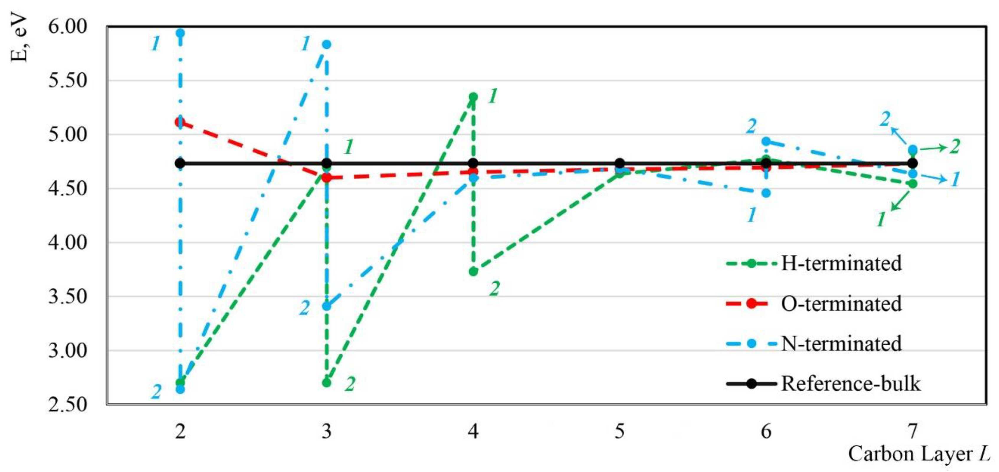
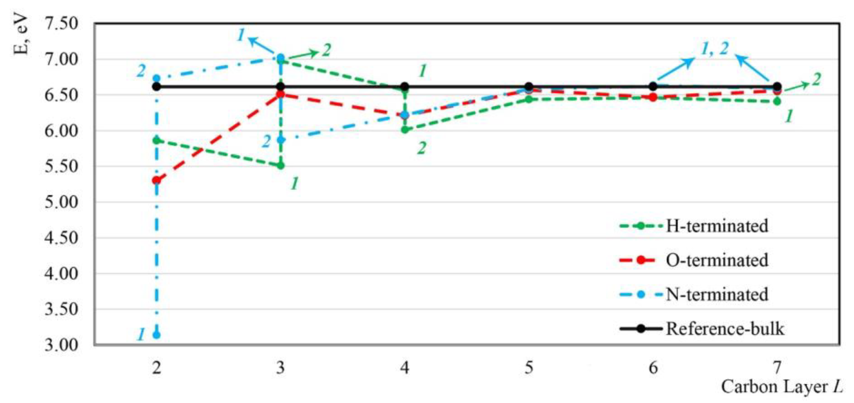
Regarding formation energy, it was generally easier for SiV 0 to be embedded in an O-terminated diamond (001) surface when this was above the fifth C layer. Formation energies were almost the same when placed below the fifth C layer among H, O, and N terminations. However, it was similarly easy for SiV 0 to form as both configuration 1 (i.e., its original (prior to geometry optimization) Si or V site was positioned in the third C layer, below the dimer rows) and configuration 2 (i.e., its original (prior to geometry optimization) Si or V site was positioned in the third C layer, between the dimer rows) at the second and to third layers under N termination, and as configuration 2 (i.e., both of its original (prior to geometry optimization) Si and V site were positioned in the third or fourth C layers, between the dimer rows) at the third and fourth layers under H termination as compared with O termination.
(3).
Si generally showed a lower formation energy than SiV near H-, O-, or N-terminated diamond (001) surfaces. However, SiV centers exhibited rather high energetic stability once formed, as indicated by their binding energies.
(4).
H termination exhibited a contracting effect on inner surface atoms. For O termination, there was a small expanding effect on inner surface atoms. Similar to H termination, N termination showed a small contracting effect on inner surface atoms.
(5).
H termination species introduced heavy impurity energy levels deep down in the CBM, and even worse, deep impurity energy levels were introduced not only above the VBM but also below CBM under O termination, in the DOS of diamond (001) surfaces. Our calculations revealed that there were almost no such impurity energy levels above the VBM or below the CBM for N termination, which indicates that an N-terminated diamond (001) surface is a suitable medium for the use of single SiV 0 as a single-photon source.

Author Contributions

Y.P. and W.S. contributed equally to this work; conceptualization, S.S. and H.L.; data curation, Y.P. and W.S.; formal analysis, Y.P. and W.S.; funding acquisition, W.S., S.S. and H.L.; investigation, Y.P. and W.S.; methodology, Y.P. and W.S.; project administration, S.S. and H.L.; resources, Y.P., W.S., S.S., and H.L.; Software, Y.P. and W.S.; Supervision, S.S. and H.L.; Validation, Y.P. and W.S.; Visualization, Y.P. and W.S.; writing—original draft, Y.P. and W.S.; writing—review and editing, S.S. and H.L.

Funding

This research was funded by the International Cooperation Research Project of Shenzhen, grant number GJHZ20180413182004161.

Conflicts of Interest

The authors declare no conflict of interest.

References

  1. Schirhagl, R.; Chang, K.; Loretz, M.; Degen, C.L. Nitrogen-vacancy centers in diamond: Nanoscale sensors for physics and biology. Annu. Rev. Phys. Chem. 2014, 65, 83–105. [Google Scholar] [CrossRef] [PubMed] [Green Version]
  2. Shen, W.; Pan, Y.; Shen, S.; Li, H.; Zhang, Y.; Zhang, G. Electron affinity of boron-terminated diamond (001) surfaces: A density functional theory study. J. Mater. Chem. C 2019, 7, 9756–9765. [Google Scholar] [CrossRef]
  3. Knill, E.; Laflamme, R.; Milburn, G.J. A scheme for efficient quantum computation with linear optics. Nature 2001, 409, 46–52. [Google Scholar] [CrossRef] [PubMed]
  4. Gisin, N.; Ribordy, G.; Tittel, W.; Zbinden, H. Quantum cryptography. Rev. Mod. Phys. 2002, 74, 145–195. [Google Scholar] [CrossRef] [Green Version]
  5. Neumann, P.; Kolesov, R.; Naydenov, B.; Beck, J.; Rempp, F.; Steiner, M.; Jacques, V.; Balasubramanian, G.; Markham, M.L.; Twitchen, D.J.; et al. Quantum register based on coupled electron spins in a room-temperature solid. Nat. Phys. 2010, 6, 249. [Google Scholar] [CrossRef]
  6. Maletinsky, P.; Hong, S.; Grinolds, M.S.; Hausmann, B.; Lukin, M.D.; Walsworth, R.L.; Loncar, M.; Yacoby, A. A robust scanning diamond sensor for nanoscale imaging with single nitrogen-vacancy centres. Nat. Nanotechnol. 2012, 7, 320. [Google Scholar] [CrossRef]
  7. Rondin, L.; Tetienne, J.P.; Hingant, T.; Roch, J.F.; Maletinsky, P.; Jacques, V. Magnetometry with nitrogen-vacancy defects in diamond. Rep. Prog. Phys. 2014, 77, 056503. [Google Scholar] [CrossRef] [Green Version]
  8. McGuinness, L.P.; Yan, Y.; Stacey, A.; Simpson, D.A.; Hall, L.T.; Maclaurin, D.; Prawer, S.; Mulvaney, P.; Wrachtrup, J.; Caruso, F.; et al. Quantum measurement and orientation tracking of fluorescent nanodiamonds inside living cells. Nat. Nanotechnol. 2011, 6, 358. [Google Scholar] [CrossRef]
  9. Le Sage, D.; Arai, K.; Glenn, D.R.; DeVience, S.J.; Pham, L.M.; Rahn-Lee, L.; Lukin, M.D.; Yacoby, A.; Komeili, A.; Walsworth, R.L. Optical magnetic imaging of living cells. Nature 2013, 496, 486. [Google Scholar] [CrossRef]
  10. Aharonovich, I.; Castelletto, S.; Simpson, D.A.; Su, C.H.; Greentree, A.D.; Prawer, S. Diamond-based single-photon emitters. Rep. Prog. Phys. 2011, 74, 076501. [Google Scholar] [CrossRef]
  11. Pezzagna, S.; Rogalla, D.; Wildanger, D.; Meijer, J.; Zaitsev, A. Creation and nature of optical centres in diamond for single-photon emission—Overview and critical remarks. New J. Phys. 2011, 13, 035024. [Google Scholar] [CrossRef]
  12. Brouri, R.; Beveratos, A.; Poizat, J.-P.; Grangier, P. Photon antibunching in the fluorescence of individual color centers in diamond. Opt. Lett. 2000, 25, 1294–1296. [Google Scholar] [CrossRef] [PubMed] [Green Version]
  13. Mizuochi, N.; Makino, T.; Kato, H.; Takeuchi, D.; Ogura, M.; Okushi, H.; Nothaft, M.; Neumann, P.; Gali, A.; Jelezko, F.; et al. Electrically driven single-photon source at room temperature in diamond. Nat. Photonics 2012, 6, 299. [Google Scholar] [CrossRef]
  14. Wang, C.; Kurtsiefer, C.; Weinfurter, H.; Burchard, B. Single photon emission from SiV centres in diamond produced by ion implantation. J. Phys. B 2005, 39, 37–41. [Google Scholar] [CrossRef] [Green Version]
  15. Neu, E.; Steinmetz, D.; Riedrich-Möller, J.; Gsell, S.; Fischer, M.; Schreck, M.; Becher, C. Single photon emission from silicon-vacancy colour centres in chemical vapour deposition nano-diamonds on iridium. New J. Phys. 2011, 13, 025012. [Google Scholar] [CrossRef]
  16. Gaebel, T.; Popa, I.; Gruber, A.; Domhan, M.; Jelezko, F.; Wrachtrup, J. Stable single-photon source in the near infrared. New J. Phys. 2004, 6, 98. [Google Scholar] [CrossRef]
  17. Rabeau, J.R.; Chin, Y.L.; Prawer, S.; Jelezko, F.; Gaebel, T.; Wrachtrup, J. Fabrication of single nickel-nitrogen defects in diamond by chemical vapor deposition. Appl. Phys. Lett. 2005, 86, 131926. [Google Scholar] [CrossRef] [Green Version]
  18. Aharonovich, I.; Castelletto, S.; Simpson, D.A.; Stacey, A.; McCallum, J.; Greentree, A.D.; Prawer, S. Two-level ultrabright single photon emission from diamond nanocrystals. Nano Lett. 2009, 9, 3191–3195. [Google Scholar] [CrossRef]
  19. Iwasaki, T.; Ishibashi, F.; Miyamoto, Y.; Doi, Y.; Kobayashi, S.; Miyazaki, T.; Tahara, K.; Jahnke, K.D.; Rogers, L.J.; Naydenov, B.; et al. Germanium-vacancy single color centers in diamond. Sci. Rep. 2015, 5, 12882. [Google Scholar] [CrossRef] [Green Version]
  20. Neumann, P.; Kolesov, R.; Jacques, V.; Beck, J.; Tisler, J.; Batalov, A.; Rogers, L.; Manson, N.B.; Balasubramanian, G.; Jelezko, F.; et al. Excited-state spectroscopy of single nv defects in diamond using optically detected magnetic resonance. New J. Phys. 2009, 11, 013017. [Google Scholar] [CrossRef]
  21. Tisler, J.; Balasubramanian, G.; Naydenov, B.; Kolesov, R.; Grotz, B.; Reuter, R.; Boudou, J.-P.; Curmi, P.A.; Sennour, M.; Thorel, A.; et al. Fluorescence and spin properties of defects in single digit nanodiamonds. ACS Nano 2009, 3, 1959–1965. [Google Scholar] [CrossRef] [PubMed]
  22. Lim, T.-S.; Fu, C.-C.; Lee, K.-C.; Lee, H.-Y.; Chen, K.; Cheng, W.-F.; Pai, W.W.; Chang, H.-C.; Fann, W. Fluorescence enhancement and lifetime modification of single nanodiamonds near a nanocrystalline silver surface. PCCP 2009, 11, 1508–1514. [Google Scholar] [CrossRef] [PubMed]
  23. Dietrich, A.; Jahnke, K.D.; Binder, J.M.; Teraji, T.; Isoya, J.; Rogers, L.J.; Jelezko, F. Isotopically varying spectral features of silicon-vacancy in diamond. New J. Phys. 2014, 16, 113019. [Google Scholar] [CrossRef]
  24. Sternschulte, H.; Thonke, K.; Sauer, R.; Münzinger, P.C.; Michler, P. 1.681-ev luminescence center in chemical-vapor-deposited homoepitaxial diamond films. Phys. Rev. B 1994, 50, 14554–14560. [Google Scholar] [CrossRef]
  25. Rose, B.C.; Huang, D.; Zhang, Z.-H.; Stevenson, P.; Tyryshkin, A.M.; Sangtawesin, S.; Srinivasan, S.; Loudin, L.; Markham, M.L.; Edmonds, A.M.; et al. Observation of an environmentally insensitive solid-state spin defect in diamond. Science 2018, 361, 60. [Google Scholar] [CrossRef] [Green Version]
  26. Vlasov, I.I.; Barnard, A.S.; Ralchenko, V.G.; Lebedev, O.I.; Kanzyuba, M.V.; Saveliev, A.V.; Konov, V.I.; Goovaerts, E. Nanodiamond photoemitters based on strong narrow-band luminescence from silicon-vacancy defects. Adv. Mater. 2009, 21, 808–812. [Google Scholar] [CrossRef]
  27. Shershulin, V.A.; Sedov, V.S.; Ermakova, A.; Jantzen, U.; Rogers, L.; Huhlina, A.A.; Teverovskaya, E.G.; Ralchenko, V.G.; Jelezko, F.; Vlasov, I.I. Size-dependent luminescence of color centers in composite nanodiamonds. Phys. Status Solidi A 2015, 212, 2600–2605. [Google Scholar] [CrossRef]
  28. Bolshakov, A.; Ralchenko, V.; Sedov, V.; Khomich, A.; Vlasov, I.; Khomich, A.; Trofimov, N.; Krivobok, V.; Nikolaev, S.; Khmelnitskii, R.; et al. Photoluminescence of SiV centers in single crystal CVD diamond in situ doped with Si from silane. Phys. Status Solidi A 2015, 212, 2525–2532. [Google Scholar] [CrossRef]
  29. Stehlik, S.; Ondic, L.; Varga, M.; Fait, J.; Artemenko, A.; Glatzel, T.; Kromka, A.; Rezek, B. Silicon-vacancy centers in ultra-thin nanocrystalline diamond films. Micromachines 2018, 9, 281. [Google Scholar] [CrossRef] [Green Version]
  30. Yang, B.; Li, J.; Guo, L.; Huang, N.; Liu, L.; Zhai, Z.; Long, W.; Jiang, X. Fabrication of silicon-vacancy color centers in diamond films: Tetramethylsilane as a new dopant source. CrystEngComm 2018, 20, 1158–1167. [Google Scholar] [CrossRef]
  31. Kim, H.; Kim, H.; Lee, J.; Lim, W.C.; Eliades, J.A.; Kim, J.; Song, J.; Suk, J. Fabrication of silicon-vacancy color centers in nanodiamonds by using si-ion implantation. J. Korean Phys. Soc. 2018, 73, 661–666. [Google Scholar] [CrossRef]
  32. Rong, Y.; Cheng, K.; Ju, Z.; Pan, C.; Ma, Q.; Liu, S.; Shen, S.; Wu, B.; Jia, T. Bright near-surface silicon vacancy centers in diamond fabricated by femtosecond laser ablation. Opt. Lett. 2019, 44, 3793–3796. [Google Scholar] [CrossRef] [PubMed]
  33. Mei, Y.; Fan, D.; Lu, S.; Shen, Y.; Hu, X. Siv center photoluminescence induced by C=O termination in nanocrystalline diamond and graphite loops hybridized films. J. Appl. Phys. 2016, 120, 225107. [Google Scholar] [CrossRef]
  34. Kohn, W.; Sham, L.J. Self-consistent equations including exchange and correlation effects. Phys. Rev. 1965, 140, A1133–A1138. [Google Scholar] [CrossRef] [Green Version]
  35. Hohenberg, P.; Kohn, W. Inhomogeneous electron gas. Phys. Rev. 1964, 136, B864. [Google Scholar] [CrossRef] [Green Version]
  36. Clark, S.J.; Segall, M.D.; Pickard, C.J.; Hasnip, P.J.; Probert, M.I.; Refson, K.; Payne, M.C. First principles methods using castep. Zeitschrift für Kristallographie 2005, 220, 567–570. [Google Scholar] [CrossRef] [Green Version]
  37. Vanderbilt, D. Soft self-consistent pseudopotentials in a generalized eigenvalue formalism. Phys. Rev. B 1990, 41, 7892–7895. [Google Scholar] [CrossRef]
  38. Perdew, J.P.; Burke, K.; Ernzerhof, M. Generalized gradient approximation made simple. Phys. Rev. Lett. 1996, 77, 3865–3868. [Google Scholar] [CrossRef] [Green Version]
  39. Monkhorst, H.J.; Pack, J.D. Special points for brillouin-zone integrations. Phys. Rev. B 1976, 13, 5188–5192. [Google Scholar] [CrossRef]
  40. Riley, D.P. Lattice constant of diamond and the C–C single bond. Nature 1944, 153, 587–588. [Google Scholar] [CrossRef]
  41. Pfrommer, B.G.; Côté, M.; Louie, S.G.; Cohen, M.L. Relaxation of crystals with the quasi-newton method. J. Comput. Phys. 1997, 131, 233–240. [Google Scholar] [CrossRef] [Green Version]
  42. Van de Walle, C.G.; Neugebauer, J. First-principles calculations for defects and impurities: Applications to III-nitrides. J. Appl. Phys. 2004, 95, 3851–3879. [Google Scholar] [CrossRef]
  43. Halicioglu, T. Calculations for defects formed on diamond surfaces. Thin Solid Films 1993, 228, 293–296. [Google Scholar] [CrossRef]
  44. O’Donnell, K.M.; Martin, T.L.; Fox, N.A.; Cherns, D. Ab initio investigation of lithium on the diamond C(100) surface. Phys. Rev. B 2010, 82, 115303. [Google Scholar] [CrossRef] [Green Version]
  45. Petrini, D.; Larsson, K. A theoretical study of the energetic stability and geometry of hydrogen- and oxygen-terminated diamond (100) surfaces. J. Phys. Chem. C 2007, 111, 795–801. [Google Scholar] [CrossRef]
  46. Shen, W.; Shen, S.; Liu, S.; Li, H.; Nie, S.; Pan, Y.; Tian, Z.; Li, Q. Binding of hydrogen to phosphorus dopant in phosphorus-doped diamond surfaces: A density functional theory study. Appl. Surf. Sci. 2019, 471, 309–317. [Google Scholar] [CrossRef]
  47. Bartell, L.S. On the length of the carbon-carbon single bond1. J. Am. Chem. Soc. 1959, 81, 3497–3498. [Google Scholar] [CrossRef]
  48. Zywietz, A.; Furthmüller, J.; Bechstedt, F. Neutral vacancies in group-IV semiconductors. Phys. Status Solidi B 1998, 210, 13–29. [Google Scholar] [CrossRef]
  49. Hood, R.Q.; Kent, P.R.C.; Needs, R.J.; Briddon, P.R. Quantum Monte Carlo study of the optical and diffusive properties of the vacancy defect in diamond. Phys. Rev. Lett. 2003, 91, 076403. [Google Scholar] [CrossRef]
  50. Chen, Y.-C.; Salter, P.S.; Knauer, S.; Weng, L.; Frangeskou, A.C.; Stephen, C.J.; Ishmael, S.N.; Dolan, P.R.; Johnson, S.; Green, B.L.; et al. Laser writing of coherent colour centres in diamond. Nat. Photonics 2016, 11, 77. [Google Scholar] [CrossRef] [Green Version]
  51. Kononenko, V.V.; Vlasov, I.I.; Gololobov, V.M.; Kononenko, T.V.; Semenov, T.A.; Khomich, A.A.; Shershulin, V.A.; Krivobok, V.S.; Konov, V.I. Nitrogen-vacancy defects in diamond produced by femtosecond laser nanoablation technique. Appl. Phys. Lett. 2017, 111, 081101. [Google Scholar] [CrossRef]
  52. Kurita, T.; Mineyuki, N.; Shimotsuma, Y.; Fujiwara, M.; Mizuochi, N.; Shimizu, M.; Miura, K. Efficient generation of nitrogen-vacancy center inside diamond with shortening of laser pulse duration. Appl. Phys. Lett. 2018, 113, 211102. [Google Scholar] [CrossRef]
  53. Mulliken, R.S. Electronic population analysis on LCAO–MO molecular wave functions. I. J. Chem. Phys. 1955, 23, 1833–1840. [Google Scholar] [CrossRef] [Green Version]
  54. Segall, M.D.; Shah, R.; Pickard, C.J.; Payne, M.C. Population analysis of plane-wave electronic structure calculations of bulk materials. Phys. Rev. B 1996, 54, 16317–16320. [Google Scholar] [CrossRef] [PubMed] [Green Version]
  55. Gali, A.; Maze, J.R. Ab initio study of the split silicon-vacancy defect in diamond: Electronic structure and related properties. Phys. Rev. B 2013, 88, 235205. [Google Scholar] [CrossRef] [Green Version]
  56. Petrone, A.; Beck, R.A.; Kasper, J.M.; Li, X.; Huang, Y.; Crane, M.; Pauzauskie, P. Electronic structures and spectroscopic signatures of silicon-vacancy containing nanodiamonds. Phys. Rev. B 2018, 98, 205405. [Google Scholar] [CrossRef] [Green Version]
  57. Kaviani, M.; Deák, P.; Aradi, B.; Frauenheim, T.; Chou, J.-P.; Gali, A. Proper surface termination for luminescent near-surface NV centers in diamond. Nano Lett. 2014, 14, 4772–4777. [Google Scholar] [CrossRef]
Figure 1. Schematic illustration of a silicon-vacancy (SiV) center in bulk diamond, with Si positioned in a split-vacancy site, showing D 3 d symmetry alongside the symmetry axis of the [111] direction. The original two C atoms are shown as white spheres and illustrated using the letter V (vacancy).
Applsci 09 05471 g001
Figure 2. Structural illustrations of the studied diamond (001) surfaces under (a) H termination, (b) O termination, and (c) N termination. Possible Si or V sites from the second to the seventh C layer (L2 to L7) near the diamond (001) surface are presented as different colored spheres.
Applsci 09 05471 g002
Figure 3. Formation energies of a single substitutional silicon impurity in various positions (in L2 to L7) near the diamond (001) surface under H, O, or N termination and in bulk diamond as a reference. The potential silicon impurity sites under different surface states are depicted in Figure 2.
Applsci 09 05471 g003
Figure 4. Formation energies of single vacancy in various positions (in L2 to L7) near a diamond (001) surface under H, O, or N termination and in bulk diamond as a reference. The possible vacancy sites under different surface states are depicted in Figure 2.
Applsci 09 05471 g004
Figure 5. Formation energies of SiV 0 in various positions (L2 to L7) near the diamond (001) surface, under H, O, or N termination and in bulk diamond as a reference. The possible silicon and vacancy sites under different surface states are shown in Figure 2.
Applsci 09 05471 g005
Figure 6. The pDOS of configurations when a single SiV 0 is positioned (a) in the third to fourth layers of an H-terminated (configuration 2) diamond (001) surface; (b) in the second to third layers of an O-terminated diamond (001) surface; (c) in the second to third layers of an N-terminated (configuration 2) diamond (001) surface; and (d) in the bulk diamond, as reference.
Applsci 09 05471 g006
Table 1. Bond lengths between different neighboring atoms in various layers for completely H-, O-, or N-terminated diamond (001) surfaces. Within the first column, X is the specific termination species, and C1 represents C atoms in the first C layer, C2 the second C layer, and so forth in a similar fashion. Sites 1 and 2 are the two different sites within the same layer, as in Figure 2.
Bond   Length   ( Å )
H-TerminatedO-TerminatedN-Terminated
Site 1Site 2Site 1Site 2
X–X 1.62
X–C11.10 1.501.53
C1–C11.62
C1–C21.54 1.541.521.59
C2–C31.531.571.541.521.57
C3–C41.521.561.541.521.57
C4–C51.521.561.541.54
C5–C61.54 1.541.551.53
C6–C71.551.541.541.541.54
C7–C81.541.541.541.541.54
Table 2. Binding energies (eV) of different SiV 0 configurations under completely H-, O-, or N-terminated diamond (001) surfaces. Numbers 1 and 2 in the second row refer to the configurations depicted in Figure 2. Si (V) in the third row represents SiV 0 in a specific position, created with its original Si (V) in the upper layer and its V (Si) in the lower layer.
H-terminatedO-terminatedN-terminated
12 12
SiVSiVSiVSiVSiV
2–31.954.303.792.686.554.837.803.813.635.26
3–44.924.523.325.315.135.476.275.843.754.58
4–55.615.033.744.225.595.275.295.01
5–64.884.99 5.085.205.064.795.425.62
6–74.704.535.135.125.275.224.945.155.315.24
Table 3. Bond lengths and bond populations of the Si–C bonds of SiV 0 for completely H-, O-, or N-terminated diamond (001) surfaces as compared with those in bulk diamond. C1 to C5 represent C atoms in the L1 to L5 C layer from the surface.
Bond Bond   Length   ( Å ) Bond Population
BulkSi–C1.980.54
0.55
0.57
H-terminatedSi–C21.850.68
Si–C32.020.65
Si–C41.940.70
Si–C52.370.22
O-terminatedSi–C12.080.45
Si–C21.970.49
Si–C31.980.57
Si–C41.910.63
N-terminatedSi–C11.940.57
Si–C22.010.54
Si–C31.960.64
Si–C42.190.40

