Article

Design and Characterization of Electrically Conductive Structures Additively Manufactured by Material Extrusion

Institute for Engineering Design, Technische Universität Braunschweig, 38106 Brunswick, Germany
*
Author to whom correspondence should be addressed.
Appl. Sci. 2019, 9(4), 779; https://doi.org/10.3390/app9040779
Submission received: 27 January 2019 / Revised: 9 February 2019 / Accepted: 18 February 2019 / Published: 22 February 2019
(This article belongs to the Section Mechanical Engineering)

Abstract

:
Multi-material additive manufacturing offers new design freedom for functional integration and opens new possibilities in innovative part design, for instance, a local integration of electrically conductive structures or heat radiant surfaces. Detailed experimental investigations on materials with three different fillers (carbon black (CB), carbon nanotubes (CNT) and nano copper wires) were conducted to identify process-specific influencing factors on electrical conductivity and resistive heating. In this regard, raster angle orientation, extrusion temperature, speed and flow rate were investigated. A variation of the raster angle (0°, ±45°, and 90°) shows the highest influence on resistivity. An angle of 0° had the lowest electrical resistance and the highest temperature increase due to resistive heating. The material filled with nano copper wires showed the highest electrical conductivity followed by the CNT filled material and materials filled with CB. Both current–voltage characteristics and voltage-dependent heat distribution of the surface temperature were determined by using a thermographic camera. The highest temperature increase was achieved by the CNT filled material. The materials filled with CB and nano copper wires showed increased electrical resistance depending on temperature. Based on the experiments, solution principles and design rules for additively manufactured electrically conductive structures are derived.

1. Introduction

Multi-material parts manufactured by additive manufacturing (AM) demonstrate a vast potential regarding the integration of several, material-specific functions due to combining multiple materials into one part without an additional joining process needed. For example, conductive materials can be combined with conventional build materials to realize conductivity inside specific areas of the part, so that the assembly and maintenance of heat radiant surfaces [1,2], 3D printed circuits [3,4] or tactile sensors [5,6] would be omitted. Whereas only few AM technologies are capable of processing multiple materials within the manufacturing process, the AM technology material extrusion (MEX) is predestinated in this regard due to its process principle (discrete material transition) [7]. In fact, only the number of extruders integrated into the MEX machine limits the number of processable materials—even within one layer [8].
Using AM technologies for generating multi-material parts enables functional integration via discrete local material variations. In addition, a specific design of material properties such as electrical resistance due to a targeted utilization of process parameters variations or part geometry [1,2,4] expands the design freedom. Hence, in contrast to traditional manufacturing processes (e.g., milling or casting), the designer has entirely new opportunities in product design. Consequently, there are two big challenges. On the one hand, the design engineer needs to be supported to ensure a consideration of these new design potentials in conceptual design. On the other hand, rules for designing conductive structures have to be established, for instance, to adjust the electrical resistance. The latter research gap is focused on in this contribution. Therefore, a simultaneous consideration of part design and process planning is crucial to leverage the advantages of AM’s design freedom [9]. A provision of specific knowledge regarding AM’s design potentials is essential for both, conceptual design (e.g., solution principles) and detail design (e.g., design rules) [10]. At present, no systematic consideration of the design potentials of multi-material AM, especially regarding electrically conductive structures, in product development is possible. There are only rudimentary frameworks [11] or general design heuristics for multi-material AM [12,13]. Moreover, design rules for MEX generally concern only geometrical restrictions [14] or consider process related influencing factors on mechanical properties [15]. However, no specific guidelines and rules for the design of additively manufactured conductive structures have been developed. Consequently, designers have no common basis on which functions such as electrical conductivity or heat radiation can be integrated in multi-material parts manufactured by MEX.
Extensive experimental investigations were conducted regarding the determination of material- and process-specific influencing factors on electrical resistance and heat resistivity. Besides other studies, especially the influence of the raster angle orientation on the resulting resistivity was analyzed to derive design principles for additively manufactured electrically conductive and heat radiant components regarding an adjustment of the resistance. Four composite materials with three different fillers (carbon black, carbon nanotubes and nano copper wires) were used as reference materials. The varied process parameters were raster angle, extrusion temperature, speed, and flow rate. The application of additively manufactured heat resistive structures is indicated by a heating surface that is incorporated into a heat-activated color-changing material by using MEX.

2. Additively Manufactured Electrically Conductive Structures

This section gives an overview of applications that utilize additively manufactured electrically conductive structures with regard to multi-material designs, in particular manufactured by material extrusion. Even though aerosol-jet and inkjet printing are widely used for 3d printed electronic devices [16], the literature overview is specific to MEX, since it provides a great variety of composite materials with different fillers, e.g., copper, carbon fibers, carbon nanotubes, graphene, and graphite [17]. Moreover, compared to ink-based additive manufacturing processes, MEX does not need a drying process after each layer. Consequently, the design freedom of ink-based processes is generally limited to surfaces of objects [18]. Therefore, MEX allows a local integration of different functions such as thermal or electrical conductivity by combining different materials. Furthermore, MEX offers process-specific levers for adjusting resistivity and, therefore, provides a great design potential regarding additively manufactured electrically conductive structures. In Section 2.2, several studies are presented that analyzed process- and material-specific influencing factors on resistivity. These can be used to adjust the resultant part properties regarding specific requirements on electrical conductivity.

2.1. Applications of Additively Manufactured Integrated Electrically Conductive Structures

Several applications for MEX demonstrate the integration of additively manufactured electrically conductive structures by using composite materials with different fillers, for example, carbon nanotubes (CNT), nano copper wires, carbon black or graphene. In the following, an overview of realized applications regarding electrical components specific to MEX is given.
Hampel et al. (2017) [4] showed the integration of electrical components by means of a 3d printed flashing circuit, for instance, a push button, resistors, and cavities for the integration of a capacitor or an LED. Furthermore, to demonstrate the potential of functional integration of additively manufactured electrical components, Reyes et al. (2018) [19] realized a lithium ion battery that is integrated into side temples of a sunglasses and used to power an LCD. They investigated different conductive fillers and degrees with a matrix of PLA (polylactic acid) regarding resistivity and printability. Liu et al. (2018) [6] gave an overview of additively manufactured tactile sensors by using material extrusion-based processes such as MEX and direct ink writing. Specific to MEX, they emphasized the challenge between high conductivity and ensuring printability through a correspondingly high proportion of the matrix material. However, the application of different flexible tactile sensors is presented by using a conductive composite in combination with a flexible material. For instance, a capacitive force sensor is realized by using a copper filled thermoplastic elastomer. In addition, strain sensors with piezo-resistive and elastic properties and multiaxial force sensors were additively manufactured by usage of a combination of TPU (thermoplastic polyurethane) and a CNT filled composite material. In comparison, Leigh et al. (2012) [5] developed a piezo-resistive and capacitive sensor using a carbon black filled PCL (polycaprolactone) filament to detect a change of electrical resistance through pressure applied on the structure. Zhang et al. (2016) [20] printed highly conductive and flexible 2D circuits made of PLA filled with graphene flakes to investigate mechanical properties and resistivity. They reached an electrical conductivity from of up to 4.76 S/cm for a composite material filled with 6 wt % of graphene flakes. Moreover, they concluded that a deformation of the printed structure sharply increases its resistance. An additively manufactured temperature sensor made of PP (polypropylene) filled with carbon black was developed by Kwok et al. (2017) [21]. They also presented a wearable flex sensor integrated in a TPU structure that change the resistance depending on the bending radius.
Furthermore, Watschke et al. (2017) [1] presented an integrated heating panel by combining a carbon black filled composite with a PLA that changes the color depending on temperature. Thus, besides a heating function, they integrated an optical signal as a design element. However, the electrical power is limited by the high resistance of both the filler (CB) and the electrical bonding as they paused the manufacturing process to embed wires. In comparison to this, Dul et al. (2018) [2] used an ABS (acrylonitrile butadiene styrene) material filled with 6 wt % CNT to design an additively manufactured heating surface.

2.2. Characterization of Electrically Conductive Composite Materials Additively Manufactured by MEX

Several studies analyze different influencing factors on electrical resistivity of parts additively manufactured by MEX. Both influencing factors regarding material composition (e.g., type and loading of fillers) and effects of the variation of process-specific factors such as extrusion temperature, raster angle or build orientation are investigated. Mostly carbon allotropes, for instance, carbon nanotubes, carbon black and graphene, are used for the functionalization of the material composites. Besides effects on electrical conductivity, certain studies underline the positive effect of fillers on mechanical properties, especially Young’s modulus and tensile strength [2,18,19,20,21,22]. Due to the direction of the deposited material, some fillers (e.g., graphene flakes) are oriented in the extrusion direction and, thus, the anisotropy of conductivity and tensile strength or Young’s modulus increases [20]. However, elongation at break decreases with increasing loading of filler, thus the fracture behavior possibly limits the maximum filler content specific to the application [2,20]. Further, a high loading of filler may restrict the printability [20]. Besides these material-specific variations, process-specific anisotropies in resistivity are also analyzed in several studies (see Table 1). Both factors of influence regarding geometry, e.g., build orientation [2,22,23,24], and with regard to process are investigated, for instance, raster angle [1,2], raster width [21], air gap or flow rate [1,21] as well as active cooling [4], extrusion speed [4], and temperature [1,4]. In addition to electrical conductivity, Watschke et al. (2017) [1] and Dul et al. (2018) [2] investigated resistive heating due to process- and material-specific variations.
In contrast to carbon allotropes, Tan and Low (2018) [18] developed highly conductive metal composites by filling PA6 (polycaprolactam—6) and HDPE (high density polyethylene) with 5–35 vol % of nickel powder and Sn95Ag4Cu1 (tin alloy) in a ratio of 2:3. They achieved conductivity of filaments from up to 31,000 S/m for the PA6 at a filler loading of 30 vol %, although, the conductivity decreased by about 25% as a result of absorbing water due to the hygroscopic effect. In comparison, the HDPE filled metal composite achieves a conductivity up to 23,000 S/m at a filler loading of 35 vol %. The composite materials are processed in a multi-material process by using PLA as the non-conductive part. The tensile strength and Young’s modulus of the PA6 filled composite materials increases, whereas the tensile strength of the HDPE filled material at a filler loading higher than 15 vol % decreases. As a result of the extrusion process, the conductivity of the processed material in the additively manufactured parts decrease significantly to 80–1850 S/m (3.3–11.6%) in horizontal direction (X/Y) and to 2–380 S/m in build direction.
Based on their experimental results, Hampel et al. (2017) [4] developed a rudimentary analytical model for the calculation of the electrical resistance of additively manufactured parts by MEX that supports designing electrical components. In addition, Zhang et al. (2017) [23] provided an approach for simulating resulting electrical resistance regarding specific process parameters by utilizing finite elements method. Furthermore, Gnanasekaran et al. (2018) [3] highlighted the challenge of combining different materials utilizing multi-material MEX as the individual thermal shrinkage results in a distortion of the multi-material part and, thus, the resulting conductivity is influenced.
The influence of electrical bonding on the resistivity is not part of the studies mentioned above; however, Kim et al. (2017) [24] postulated the suitability of silver paste.
Based on the literature review, this contribution aimed at the investigation of material- and process-specific design opportunities for an adjustment of resistivity and heat radiation capacity of additively manufactured parts. It focused on the comparison of different fillers and process parameter sets, in particular raster angle orientation. From this, both design principles for the integration of electrically conductive structures or heat radiant surfaces and advice for its design are presented.

3. Experimental

In this section, the experimental set-up is presented with regard to the design of experiments and used test methods and specimens. Moreover, the utilized AM-machine, the manufacturing of the test specimens and preliminary experiments regarding different concepts of electrical bonding are described.

3.1. Experimental Set-Up

3.1.1. Test Specimens, Methods and Design of Experiments

Table 1 shows that much research is carried out in material development. However, the listed studies investigate only isolated process-specific influencing factors on resistivity. In addition, the studies do not derive design principles or rules to support the design of additively manufactured conductive structures or heat radiant surfaces. Therefore, in this contribution, two different specimens were developed to determine process- and material-specific variations of resistivity regarding two of the main applications: electrical conductors and heat radiating surfaces (see Section 2.1). The first specimen for the characterization of the resistance was inspired by the form of an electrical conductor (see Figure 1), whereas the second specimen was much broader and formed as a flat rectangle (see Figure 2) to reproduce a heat radiating structure. As the raster angle orientation regarding the adjustability of resistivity is hardly considered in the studies mentioned above, it was focused in in this contribution. Solely, Watschke et al. (2017) [1] investigated specifically the influence of different infill patterns on resistivity and found that it provides a vast potential for adjusting the resulting resistance of additively manufactured structures. Indeed, they only analyzed the carbon black filled material Proto-pasta Conductive PLA [25]. Consequently, a transferability of the results to other materials with different fillers is not examined.
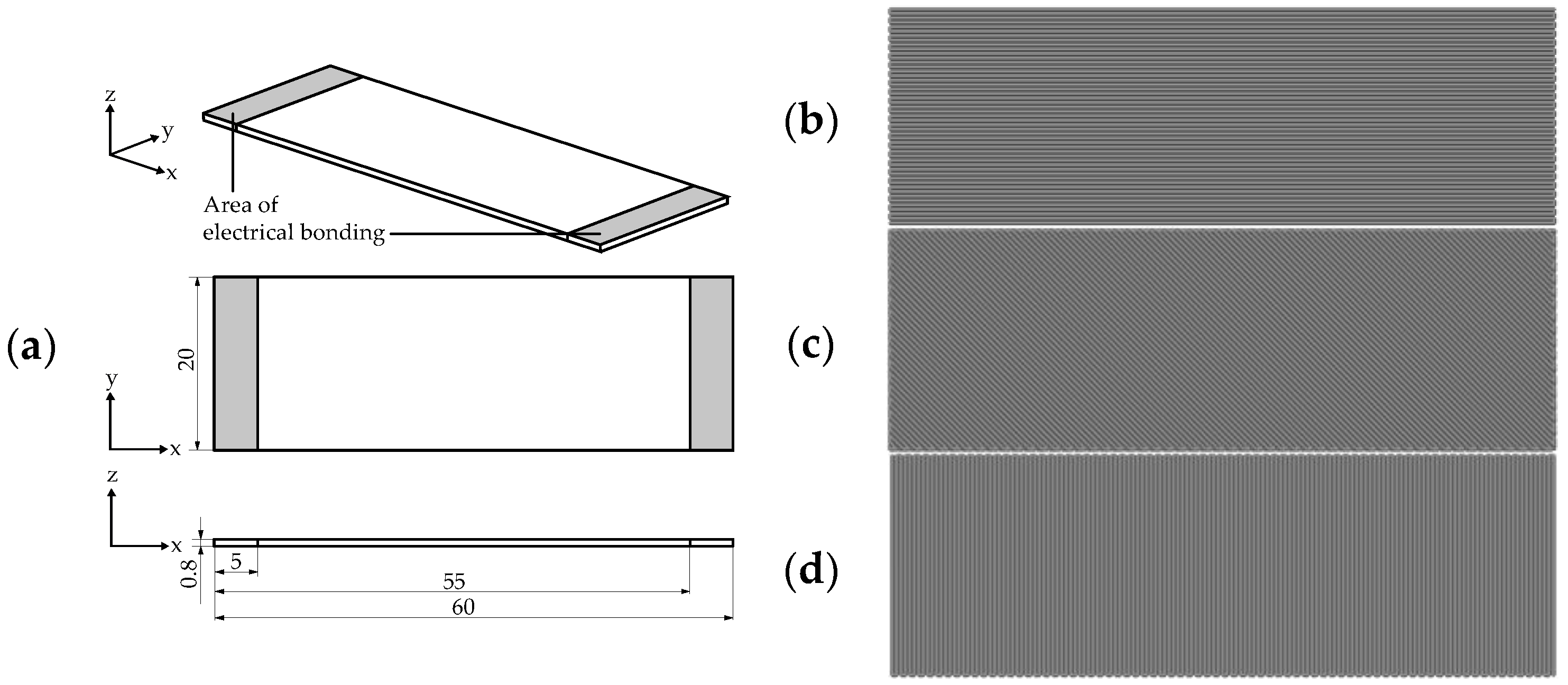
Figure 1a shows the specimen and its dimensions for the characterization of resistivity of different process parameter sets. The resistance was measured between the areas of electrical bonding that are highlighted in grey. Since, according to Hampel et al. (2017) [4] and Watschke et al. (2017) [1], the infill pattern has a strong influence on the electrical resistance due to the varying number of strand boundaries, the raster angle orientation was explicitly taken into account in the experimental investigations. To determine solely the influence of the raster angle orientation, the perimeter shells were disabled in the slicing process. The resulting trajectories of the used raster angle orientations of 0°, ±45° and 90° are represented in Figure 1b–d. The specimens were directly processed on object slides (see Section 3.1.2).
Figure 2 shows both the dimensions of the specimen for the experimental investigation of the heat radiation capacity and the trajectories used for the additive manufacturing process. The dimensions are similar to the specimen shown in Figure 1. The height (0.8 mm) as well as the overall length (60 mm) and length between the electrical bonding (50 mm) are identical. Since the homogeneity of both the heat radiation and the heating of the specimen were analyzed, the width of the specimen was chosen as 20 mm. Thus, the manufacturability on an object slide was still possible to ensure equal boundary conditions for the manufacturing. Because of the increased width, the effect of the AM-machine’s acceleration at the boundary was less for the resistivity of the overall structure.
As many materials with different fillers are available for MEX, the following four different material composites were exemplarily chosen for the design of experiments: Proto-pasta Conductive PLA (PPC) [25], 3dkonductive PLA (3dk) [26], Functionalize F-Electric™ PLA (FFE) [27], and MULTI3D Electrifi Conductive Filament (M3D) [28] (see Table 2). Thus, three different fillers were investigated to determine their process parameter specific influence on resistivity. Both PPC and 3dk use as filler CB and, therefore, have a significant higher resistance than the CNT (FFE) and copper filled material (M3D). Thus, by utilizing these materials, various design opportunities were possible, e.g., electrical conductors, heat radiation surfaces, or flexible sensor (cf. Table 1). Besides information about feedstock material’s resistivity, Table 2 also shows the processing conditions of the individual materials.
Table 3 presents the design of experiments for determining material- and process-specific dependencies of resistivity. The variation parameters were selected based on the literature review and the ranges of the individual process parameters in accordance with the processing conditions shown in Table 2. Even though other parameters such as line width or overlap also influence the compaction between layers and thus resistivity, these parameters were not considered in this contribution due to the increased scope of the experimental investigations. The maximal extrusion temperature was chosen as 10 °C above the recommended temperature. It has to be noted that the materials FFE and M3D are not processable below an extrusion temperature of 220 °C or 170 °C caused by a low flowability (see Figure 3). Therefore, the minimal extrusion temperature was set to 220 °C for FFE and 170 °C for M3D. Besides the extrusion temperature, high speed may also result in defects and, thus, in a damaged specimen, thus the maximum speed was set to 60 mm/s. It is worth noting that the range of process parameters can be increased by changes in manufacturing conditions, for example, varying build platform temperature or using additional types of adhesives.
A full fractional parameter variation was chosen for each material. Thus, 351 batches each with three specimens were manufactured. Consequently, in total, 1053 specimens were additively manufactured in the selected design of experiments. The conditions of manufacturing are described in detail in Section 3.1.2. The design of experiments was limited to the determination of resistivity (cf. specimen shown in Figure 1). The measurement of the heat resistivity was solely conducted with selected process parameter sets that exhibit low electrical resistance. These specimens were defined based on the experimental investigations regarding resistivity.
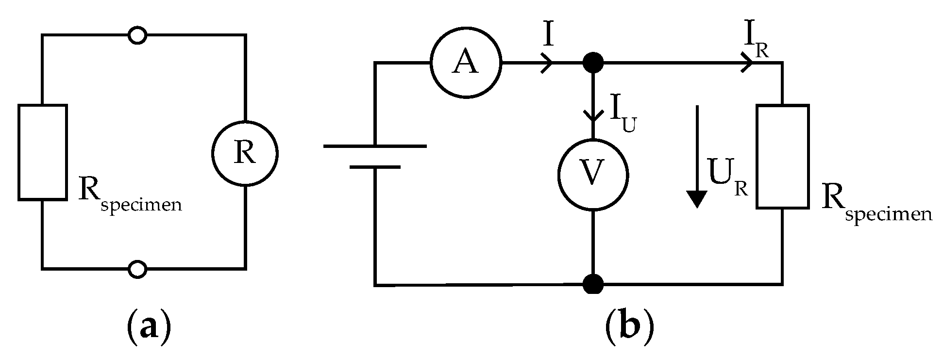
The different test set-ups represented in Figure 4 were used to determine the electrical resistance of the two presented test specimens for electrical resistivity and heat radiation capacity. The testing was carried out at ambient temperature of 23 ± 1 °C and a relative humidity of 45–50%. For the measurement of the resistance of the specimens shown in Figure 1, the test set-up shown in Figure 4a and a VOLTCRAFT MT-52 (Conrad Electronic AG, Wollerau, Switzerland) were used.
The experimental set-up for the determination of the current–voltage characteristics is shown in Figure 4b. The maximum applied voltage depends on the resulting electrical capacity that damages the specimens when exceeding the heat deflection temperature of the matrix material due to resistive heating. The material- and process-specific maximum voltage was determined in preliminary investigations for each specimen. A VOLTCRAFT VLP 2403pro was used as a direct current (DC) power supply. Further, a VOLTCRAFT MT-52 (Conrad Electronic AG, Wollerau, Switzerland) was used for measuring the voltage U and the current I was measured by a VOLTCRAFT VC-110 (Conrad Electronic AG, Wollerau, Switzerland). The resulting resistance of the specimen was determined according to Equations (1) and (2), where Rimpedance is 10 MΩ:
R specimen = U R I I U
I U = U R R impedance
The calculation of the resistivity was carried out using Equation (3), where R is the measured electrical resistance, A the cross-section of the test specimen, and L the distance between the areas of electrical bonding:
ρ = R A L
Besides the resistive current–voltage characteristics, the surface temperature generated by resistive heating was measured by a VarioCAM® HD head 800 thermographic camera (InfraTec GmbH, Dresden, Germany) with the software IRBIS® 3. To determine the heat distribution, the surface temperature was measured at different voltages individually for each material and process parameter set.

3.1.2. Machine and Manufacturing of Test Specimens

Material extrusion was chosen for the manufacturing of the test specimens, since multi-material MEX allows a combination of multiple materials for incorporation electrically conductive structures. MEX uses thermoplastic polymers as feedstock materials that are directed into an extruder unit where the material is melted. The plasticized material is applied to a build platform or previous layer according to the individual cross section of the generated part. Due to thermal fusion, the applied layer bonds with the surrounding already solidified material. In this way, the part is generated layer by layer [8]. The process of multi-material MEX was shown and described in more detail, for example, by Watschke et al. (2018) [29]. For manufacturing of the specimens, the pro-consumer machine X400 by German RepRap GmbH (Feldkirchen, Germany) with a dual extruder system was used. The printer comes with a heated build platform and a direct extruder with a nozzle diameter of 0.4 mm. For the preparation of the build job, the slicing software Simplify3D (version 4.0) was used. Table 2 gives an overview of the utilized process parameter sets. In addition, the line width was set to 0.4 mm and no perimeter shells were used. The material was directly processed on object slides that were positioned in recesses in a sheet metal (see Figure 5). In the sheet metal, three object slides can be positioned. On each object slide, three test specimens were printed with the same set of process parameters. In one build job, three batches were manufactured one specimen after another to ensure repeatable process conditions. In addition, solely the extrusion speed varied in one build job, whereas extrusion temperature, flow rate, and raster angle orientation were equal. All specimens were manufactured by using the identical calibration set-up and the same environmental conditions (ambient temperature of 23 ± 1 °C and a relative humidity of 45–50%).
Due to this experimental set-up, the specimens did not have to be removed from the build table after the manufacturing process, thus damage due to the removal was avoided. Further, the electrical bonding and the measurement of the electric resistance was conducted without detaching the specimens from the object slides. Thus, the repeatability of both the manufacturing process and the characterization of the specimen’s resistance was improved. The specimens for analyzing heat radiation capacity were also directly processed on object slides.
Before starting the manufacturing process, the materials were dried: the materials based on PLA at 45 °C and M3D at 30 °C, for 4 h each. To ensure equal environmental conditions during the printing process, the materials were stored in a box during the manufacturing process that regulates relative humidity at about 20%. Before testing, all specimens were stored at an ambient temperature of 23 ± 1 °C and a relative humidity of 45–50% for at least one week in the laboratory.

3.2. Preliminary Investigations on Electrical Bonding

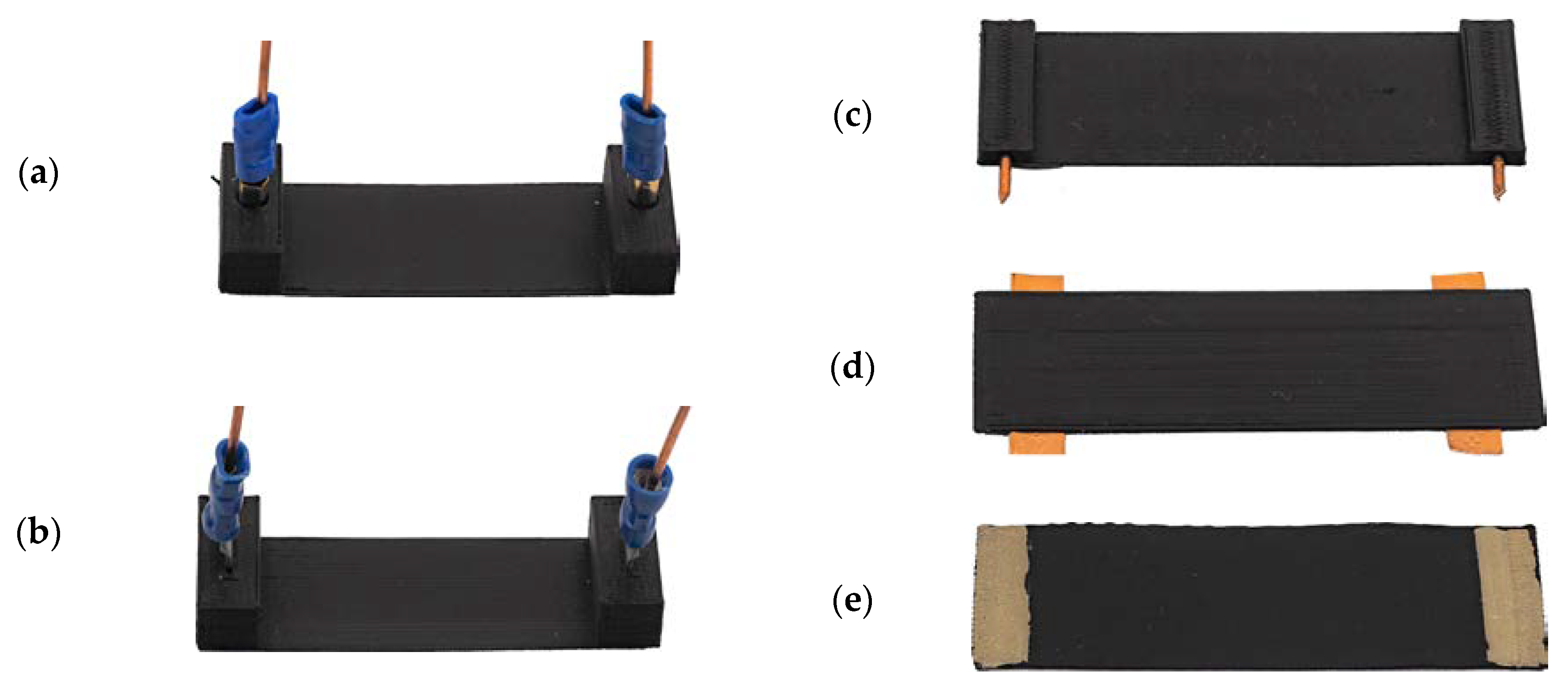
To determine the influence of electrical bonding on the resulting resistance, different concepts for applying electrical bonding were investigated. The dimensions of the test specimen were chosen as 60 × 20 × 0.8 mm3 (see Figure 2). However, the area of electrical bonding was restricted to an area of 5 × 20 mm2 on both sides on the upper side of the specimen; the length varied slightly between the individual concepts. The different concepts of electrical bonding are represented in Figure 6, whereas Table 4 shows an overview of the investigated variants in comparison to the test specimen without any additional electrical bonding concept. FFE was exemplarily tested by using the following process parameters for manufacturing: a raster angle of 0°, an extrusion temperature of 230 °C, a speed of 40 mm/s, a layer height of 0.2 mm and a flow rate of 100%. It is worth noting that the pressed-in electrical bonding concepts (no. a–c) and the specimen without electrical bonding showed a high dependence of the resulting resistance on the applied pressure during the measurement. Therefore, these variants were not suitable for the following experimental investigations as the varying resistance of the electrical bonding would significantly falsify the measurements.
The results represented in Table 4 show a vast range of resulting resistance from 50.5 Ω (silver paste) to 1504 Ω (copper wire) depending on the utilized concept of electrical bonding due to the contact resistance. In comparison to the different variants of electrical bonding, the specimen without electrical bonding had significantly higher resistance and scattering. Hence, the selection of the electrical bonding variant is a key factor in additively manufactured conductive structures, since it influences the resistance decisively. Thus, for the experimental investigation presented in Section 4, the silver paste (e) was used due to the very low bonding resistance and its easy application.
To analyze the influence of the silver paste on the resulting resistivity, the feedstock materials of the used materials PPC, 3dk, FFE and M3D were bonded along the filament strand. The distance between the measuring points was selected as 20 mm and the total measurement distance was set to 270 mm. A total of three filament strands per material were examined to determine the mean value and the standard deviation. Figure 7 shows the results of the experimental investigations. It can be seen that the electrical bonding positively influences resistivity of the feedstock material, with M3D being an exception. Furthermore, the determined resistivity of PPC, 3dk and FFE is lower than the manufacturer information suggests, while M3D’s resistivity is significant higher (see Table 2). For PPC and FFE, the influence of the electrical bonding on the resistance is very low above a measuring length of 40 mm, whereby its influence on PPC is lower as the resistivity is higher compared to FFE. In contrast, the negative influence of the electrical bonding on the resistivity of the M3D material is visible until 200 mm. In general, 3dk shows a more irregular behavior of resistance along the measuring distance masking the influence of the electrical bonding. Overall, the influence of the electrical bonding on the resistivity of the feedstock material is already negligible from a measuring distance of 40 mm. Consequently, the proposed specimens and the electrical bonding concept were suitable for the experimental investigations.

4. Results and Discussion

In this section, the results of the experimental investigations of both resistivity and heat radiant capacity depending on process parameters and fillers are presented and discussed.

4.1. Analysis of Influencing Factors on Resistivity

The influencing factors on electrical resistivity were determined by utilizing the test specimens shown in Figure 1 and the test set-up represented in Figure 4a. Before testing, the conductive silver paste EMS 12640 (Electron Microscopy Sciences, Hatfield, PA, USA) was applied and dried for at least 12 h.

4.1.1. Filler and Raster Angle Orientation

Figure 8 shows an overview of the batches with the lowest resistivity of each material and raster angle orientation. It can be seen that the standard deviation is quite low so that the repeatability of the manufacturing process is ensured. However, it has to be noted that only three specimens per batch were manufactured. In general, the resistivity is lowest for the raster angle orientation 0°, followed by ±45° and 90°. These results are to be expected due to the higher interlayer resistance according to the resistance model developed by Hampel et al. (2017) [4]. Consequently, the raster angle provides a vast potential for adjusting the resistivity of additively manufactured electrically conductive components. Further, the resulting resistivity strongly depends on the filler. For example, for a raster angle of 0°, the resistivity of the copper-based material M3D is about 450 times less than of 3dk, is approximately 240 times less than PPC, and about 30 times less than FFE. In addition, the anisotropy of M3D’s and FFE’s resistivity regarding the raster angle of 0° compared to ±45° or 90° is higher than that of the CB filled materials PPC and 3dk. This fact probably results from an orientation of the filler particles in the extrusion direction. This presumption was supported by Tekinalp et al. (2014) [31] who found a high fiber orientation in the extrusion direction for carbon fiber–polymer composites and Zhang et al. (2016) [20] who observed an increase of the conductivity during the extrusion process.
The resistivity of the selected additively manufactured specimens made of PPC and FFE are higher compared to their feedstock materials, whereas for 3dk and a raster angle of 0° the resistivity is almost identical. Compared to that, the specimen’s resistivity made of M3D is significantly higher than of the feedstock material in all raster angle orientations (cf. Figure 7).

4.1.2. Extrusion Temperature, Speed and Flow Rate

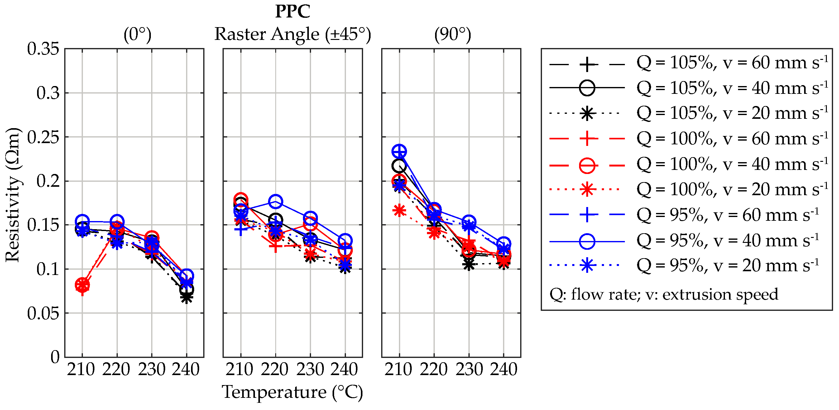
Figure 9 shows the examined influencing factors on resistivity for PPC structured by raster angle orientation. It can generally be seen that, besides the raster angle, the extrusion temperature strongly influences the resulting resistivity. Thus, the higher energy input probably results in both a lower inner-bead porosity and inter-bead porosity due to the molecular diffusion of the polymer chains within the interface zone between the strands [31,32]. The grown interface zone (neck) leads to a lower resistivity. In general, this effect is lower for a raster angle of 0° most likely due to less inner-bead porosity and for the infill pattern of ±45° probably due to a higher inter-bead porosity because of an intersecting of the extruded strands. Furthermore, lower speeds also result in lower resistivity due to a higher energy input and probably a higher accuracy and, thus, less porosity. However, a detailed analysis of the influence of the parameters regarding porosity, and thus resistivity, was not conducted and has to be done in further experimental investigations. It has to be noted that, because of the turnaround points for the raster angles of ±45° and 90°, the maximum speeds of 40 mm/s and 60 mm/s were likely not reached due to the machine’s acceleration. The resistivity is also influenced by means of a variation of the flow rate. By using a raster angle of 90°, an underextrusion (flow rate of 95%) results in a slightly increased resistivity, whereas at 0° and ±45° no clear tendencies are visible. The statistical outliers for a raster angle of 0° and a flow rate of 100% cannot be explained now and require additional subsequent investigations.
In general, the resistivity of 3dk is significantly higher than of PPC, even though the filler is identical. This probably results from a difference in filler content and defects in the filament strand that occur as a result of the pressure of the feed mechanism. The resulting defects that occurred in the filament strand after extrusion are shown in Figure 10. Consequently, voids inside, along and between the beads exist and, thus, the electrical resistance increases due to the higher porosity. Both a high extrusion temperature and to a lesser extent a low speed positively influence the resistivity due to a higher energy input that results in smaller inner-bead and inter-bead voids (see Figure 11). In comparison to that, the influence of flow rate and raster angle are rather low because of defects in the filament strand.
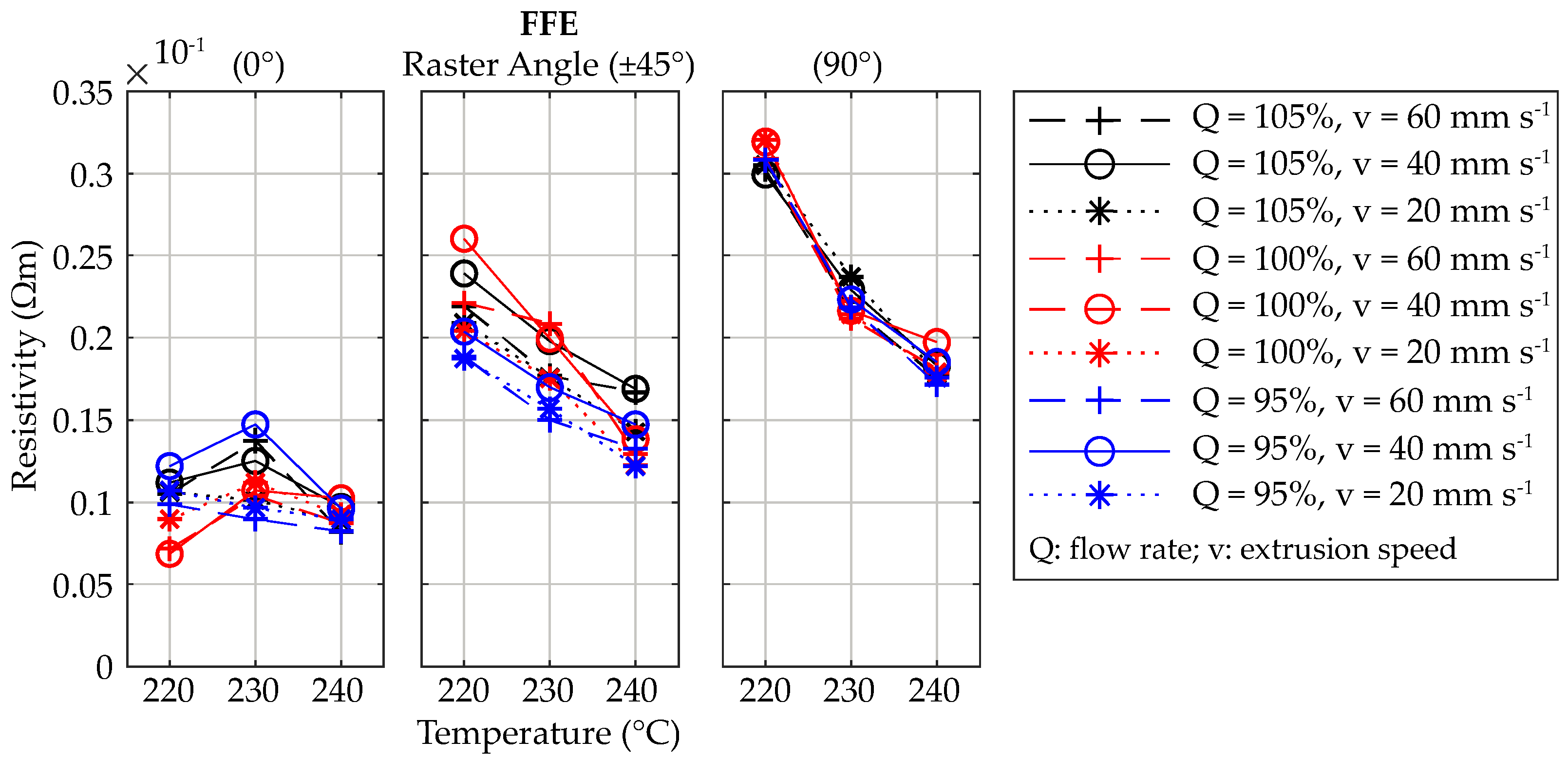
Because of the different filler (CNTs), the FFE shows a significant lower resistivity than the two CB filled materials. An overview of the dependencies of the resistivity is represented in Figure 12. Overall, raster angle orientation has the greatest influence on resistivity followed by extrusion temperature except for raster angle 0°. It is assumed that the effect of an orientation of the carbon nanotubes along the extrusion direction mainly determines the resistivity for the raster angle orientation of 0° and, as a result from this, the temperature has hardly any influence. The lower resistivity of the batches with the process parameter sets of a temperature of 220 °C, a flow rate of 100%, and speeds of 40 or 60 mm/s is probably due to the higher shear forces, which can be transmitted by the higher viscosity of the melt. However, this effect does not occur at flow rate of 95% and 105% so that defects owing to under- or overextrusion are presumed. Whereas at a raster angle of 90° both speed and flow rate solely slightly influence the resulting resistivity, these parameters for orientations of 0° and ±45° provide possibilities for adjusting electrical resistance. At a raster angle of ±45°, a flow rate of 95% tends to result in a lower resistance.
Figure 13 represents the results of the experimental investigations regarding M3D. The resulting resistivity is significantly lower than of the other characterized materials. However, an increase of extrusion temperature results in a higher resistivity, which is contrary to the results of the other experimental investigations. This is due to oxidation of the copper nanowires that are used as filler in the M3D material. According to the manufacturer of the material, the problem of filler oxidation is known, and further development of the material by an additional coating is already planned. Consequently, as extrusion speed is decreased at raster angles of ±45° and 90° owing to machine’s acceleration at the turnaround points, both the thermal damage of the filler and the resistivity increases. In general, lower speeds and lower flow rates negatively influence resistivity due to thermal damage or voids among the beads. In addition, at these flow rates, thermal conductivity of the additively manufactured structures is higher due to internal porosity because the oxidation is likely to be intensified. The range of electrical resistance at ±45° regarding flow rate and extrusion speed is very high. Since PCL has a low melting point and thermal conductivity of the composite polymer is increased due to the filler, an overextrusion results in dense layer bonding and, thus, generally in lower resistivity independent of the raster angle orientation. A low extrusion temperature and a high extrusion speed with few turnaround points (e.g., raster angle of 0°) results in less thermal damage, but can also lead to defects due to insufficient flowability of the material (see Figure 3). These defects result in an increase in resistance and a reduction in current density.
Overall, it can be stated that electrical resistance or resistivity of additively manufactured structures can be adjusted by means of the raster angle orientation as well as the process parameters extrusion temperature, speed and flow rate. Raster angle orientation has the biggest influence on resistivity, followed by extrusion temperature. In general, a raster angle of 0° results in the lowest resistivity, whereas a higher extrusion temperature also leads to decreased resistance except for M3D. Flow rate and speed have a lesser influence; however, a variation of these parameters can also be utilized for an adjustment of resistivity of additively manufactured structures. However, it has to be noted that only three specimens per batch were manufactured and both reproducibility and dependency on geometry have to be investigated in more detail, for example, regarding standard deviation.

4.2. Heat Resistivity

The properties regarding heat resistivity of the different materials and raster angle orientations were examined using selected process parameter sets based on the results of the experimental investigations presented in Section 4.1.1 (see Table 5). For these experiments, the specimens represented in Figure 2 and the test set-up shown in Figure 4b were utilized. The testing was carried out at ambient temperature of 21 ± 1 °C and the specimens were positioned on an insulation panel. To ensure comparability with the previous experimental findings, the specimens were again directly processed on object slides.
In general, compared to the experiments regarding resistivity presented in Section 4.1, the resulting resistivity of the wider specimens used for these investigations regarding resistive heating is higher. Thus, a quantitative comparison of the results in Section 4.1 and Section 4.2 is not possible. However, the influence of the raster angle orientation and the different fillers is equally obvious.

4.2.1. Heat Distribution

The heat distribution was determined along the length (50 mm) of the specimen between the electrical bonding. The heating curves were recorded after the heat distribution reached a stationary state. Figure 14 shows the heat distribution along this measuring distance for the four materials PPC, 3dk, FFE and M3D depending on the applied voltage each with the different raster angle orientations. The maximum voltage differs between the individual materials depending on the damage of the specimen caused by its softening due to resistive heating. Because of the lower resistance of FFE and M3D, the voltage was restricted to 12 V. In addition, the latter softens at much lower temperatures than the PLA-based materials due to the low melting point of its matrix polymer PCL (≈60 °C).
Due to the softening, the specimen was locally damaged and, thus, the maximum temperature was restricted to 43.5 °C and a narrow area (see Figure 15). In general, the temperature drop at both sides of the clamping was caused by the much higher thermal conductivity at the electrical bonding. Consequently, the heat was transmitted more quickly to the environment and via the cables. This results in a high thermal gradient along the measurement distance due to the comparatively low lengths of the test specimens.
Overall, the FFE specimens show the highest temperature increase of 88.5 K for the raster angle of 0°, even though the voltage was restricted to 12 V. It is followed by PPC and 3dk as higher voltages were applied. The maximum temperature of M3D is limited by the softening of the matrix polymer and, owing to this, only reaches a temperature increase of 23.5 K. Furthermore, FFE exhibits a more homogenous heat distribution compared to the other tested materials. This probably results from a higher thermal conductivity of the CNT filled composite polymer compared to the CB filled materials and, thus, a lower temperature gradient.
The influence of the raster angle orientation on the heat resistivity is most evident for FFE; however, this dependence was also observed with the other materials. Heat radiation capacity is highest at a raster angle orientation of 0°, followed by ±45° and 90°; however, 3dk is an exception as the resistance of the specimen with an infill pattern of 0° is increased in extrusion direction due to the defects in the filament strand. The heating curves of the PPC show a smaller range for the different raster angles due to a higher temperature increase of the 90° specimen from 24 V to 30 V as the glass transition temperature is exceeded. This most likely results from annealing because the resistance between the individual strands is decreased by a neck growth. 3dk does not show this effect because the glass transition temperature was not reached. FFE shows the highest dependency on the raster angle orientation, whereby the 90° oriented specimen has a significantly lower maximum temperature than the other infill patterns. At a voltage of 12 V, its temperature increase is only 56.2 K compared to 76.3 K (±45°) and 88.5 K (0°). Thus, it is very likely that the resistance is mainly determined by the orientation of the CNTs. Although the sample was clearly deformed during heating (see Figure 16), no damage could be detected, so that a homogenous temperature distribution still occurs.

4.2.2. Dependencies of Currencies, Electrical Power, and Resistance on Voltage

To analyze the dependencies of current, electrical power and resistance on voltage similar to heat distribution, only one specimen per process parameter set was tested. The test specimens were manufactured by using the same process parameter sets and the same batch of material. Due to process-related inaccuracies in the manufacturing of the specimens, the initial individual resistances of the utilized specimens in Section 4.2.1 and Section 4.2.2 vary and, thus, are not quantitatively comparable.
Each specimen was tested three times to determine mean and standard deviation. Before testing, the specimens were energized two times by the previously determined individual maximum voltage for 15 min each. This is because exceeding the glass transition temperature of the matrix polymer due to resistive heating leads to an annealing of the specimens that changes the resistance of the specimens. During cooling, the specimens were taken from the measurement set-up so that no clamping restricts their shrinkage and, thus, damages them. Based on the results in Section 4.2.1, the following maximum voltages were used for the experimental investigations of the different materials and raster angle orientations: PPC (0°, ±45° and 90°) 30 V, 3dk (0°, ±45° and 90°) 40 V, FFE (0°) 12 V, FFE (±45°) 12 V, FFE (90°) 20 V, and M3D (0°, ±45° and 90°) 6 V.
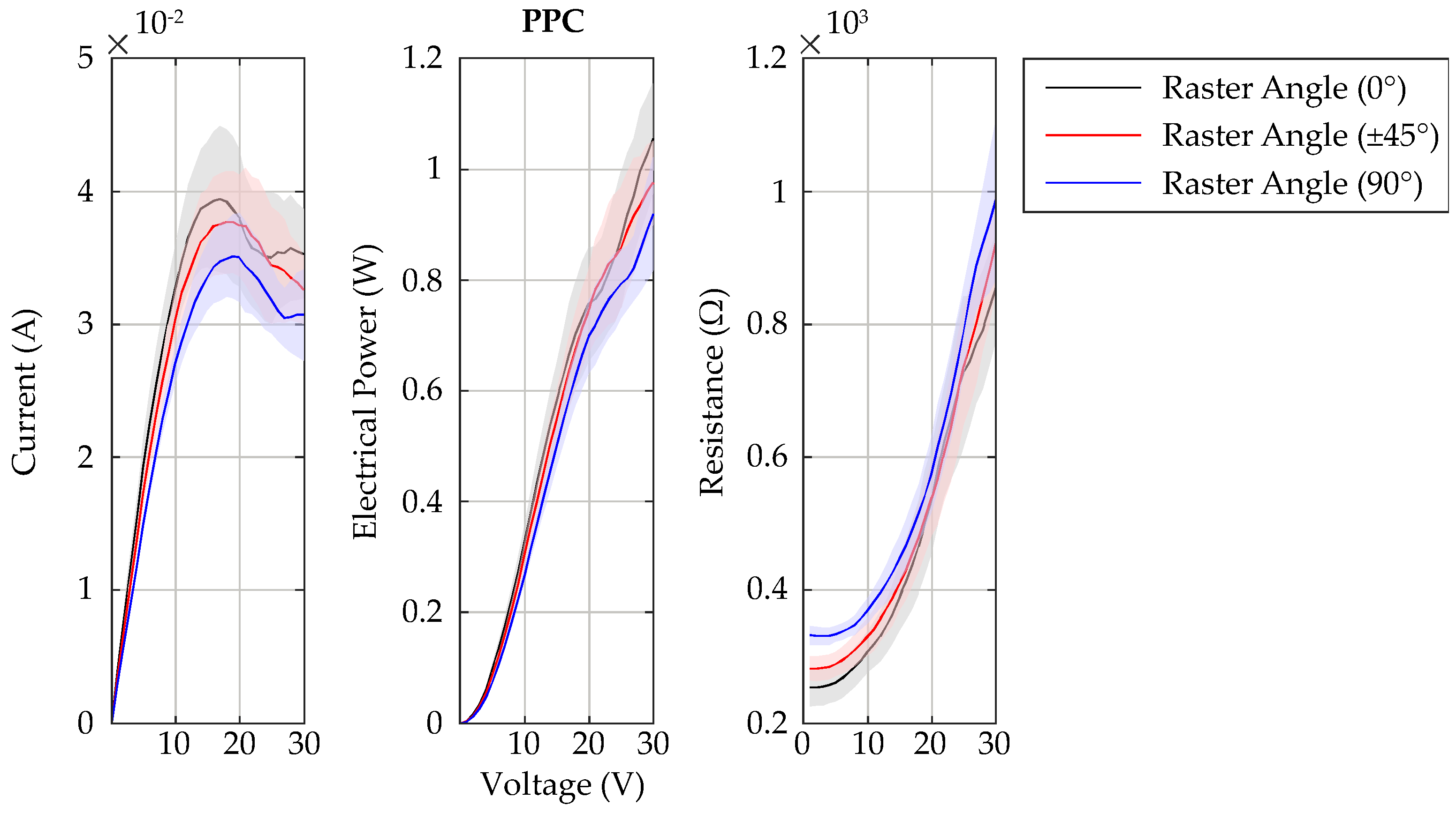
Figure 17 shows PPC’s current–voltage characteristics and the dependencies of the electrical power and the resistance on the voltage. Besides the mean value, the standard deviation of the three measurement cycles is represented for each raster angle orientation. Electrical current reaches a maximum between 15 V and 20 V depending on the raster angle due to the different resistance of the specimens. From about 5 V to 18 V, electrical power is almost linear. The decrease of current is caused by an exponential increase of the resistance depending on specimen’s temperature due to resistive heating that is shown in the right diagram. Resistance increases by a factor of about 3 between 0 V and 30 V, however, electrical power rises with increasing voltage. As in the previous investigation regarding resistivity, the dependency of specific values on the raster angle is visible, even though the difference between the raster angles of 0° and ±45° is lower than to 90°. The scattering is high compared to the other materials. This is caused by a decrease of the specimen’s resistance between the individual measurement cycles probably due to a further annealing of the specimen by exceeding the glass transition temperature.
The power–voltage characteristics of 3dk are almost linear in a range from about 12 V to 40 V (see Figure 18). Due to the higher resistance of 3dk compared to PPC, the resulting current and, thus, electrical power is lower. Consequently, the heating temperature of the specimens is also lower than the glass transition temperature of the matrix material (PLA) so that no annealing occurs that could change the resistance of the specimens. Therefore, the scattering of the values is significantly lower compared to PPC. Furthermore, the current does not fall within the measuring range, however, an approximation to a maximum value similar to PPC is noticeable at about 40 V. The temperature dependency of the resistance due to the filler (CB) is also visible. It is worth noting that the resistance of the 0° raster angle is higher than that of ±45° and 90°, which does not correspond to the results in Section 4.1.2 (Figure 11). This is probably caused by defects in the filament strand due to the pressure in the feed mechanism (see Figure 10).
Due to the filler-related low resistance of the FFE material, the maximum voltage is limited to 12 V for a raster angle of 0° and ±45° and to 20 V for the 90° infill pattern. Compared to PPC, the electrical power of the FFE at 12 V is about factor 8 (0°), 6 (±45°), or 3 (90°) higher (see Figure 19). The power–voltage characteristics have an almost exponential increase in contrast to PPC and 3dk. The dependence of the raster angle orientation is obvious for current, electrical power and resistance. Especially for a raster angle of 90°, the resulting resistivity is higher than in the experimental investigations presented in Section 4.1. This probably results from the larger material output and higher energy input at the turnaround points that affects resistivity positively as the width of the specimen is low and, thus, is the time span between two adjacent strands to cool down. Resistance does not depend on the temperature in contrast to PPC and 3dk. However, it slightly increases due to a softening of the specimen if the glass transition temperature of the matrix polymer (PLA) is exceeded.
In Figure 20, the experimental results of M3D are represented. The current–voltage curves of the 0° and the ±45° raster angle have a high gradient and sharply decrease shortly above 3 V compared to the other materials. Consequently, the electrical power is limited to about 0.4 W as the resistance steeply increases due to softening of the PCL. The resulting damage is clearly visible in Figure 15. Due to this damage, the standard deviation of current, electrical power and resistance before softening is comparatively high. After softening the standard deviation is significant lower. Although the resistance after the damage increased, it is compared to the other materials still low. Moreover, the maximum current of the 90° oriented specimen is significant lower, most likely by the fact that the softening between the processed strands earlier influences resistance. However, it is not clear why resistance briefly stagnates between 2.5 V and 3.5 V before rising again.

4.3. Derivation of Design Principles

Based on the experimental results in Section 4.1 and Section 4.2, several design principles for the utilization of both electrically conductive and heat resistive structures manufactured by AM can be derived. By incorporating electrically conductive materials in a standard polymer such as PLA or another functional material, for example, shape memory or color-changing polymers, several functions can be integrated using multi-material MEX. In addition, these functionalities can be adjusted by the choice of matrix polymer and filler as well as geometry and process parameters. Table 6 shows an overview of selected design principles derived based on the experimental investigations. Besides the utilized effect, AM-specific levers and advice for design are indicated to facilitate both an application and an implementation of the design principles in product design.
Based on the experimental results in Section 4.1, the resulting resistance of an additively manufactured structure can be adjusted by both geometry and process parameters. Especially the length and cross section as well as the raster angle orientation and the extrusion temperature. In addition, the filler and its content significantly influence the resistivity of the feedstock material, but also change the mechanical properties. Consequently, there are many possibilities to realize the required resistance depending on the application. However, the process parameters interact with the geometry of the part, which is why the determined resistivity of narrow structures (e.g., electrical conductors) is not directly transferable to broader geometries such as a heating surface.
Due to its high conductivity and the low melting point of the matrix polymer PCL, M3D is suitable, e.g., for the manufacturing of electrical fuses, as resistance sharply increases when PCL softens. The electrical power that results in a softening of the structure can be adjusted by the raster angle orientation and the structure’s dimensions (cross section and length) as well as the filler. However, for a repeatable application, it is required that the softening process is reversible and the initial resistance of the structure does not change, for example, due to a continual damage.
The material- and process-specific resistance heating can further be utilized to realize a heating surface with varying heat radiation by using locally different process parameter sets, for example, raster angle and extrusion temperature or combining materials with different fillers. Temperature can also be adjusted by variation of the applied voltage. When incorporating a heating surface into an additively manufactured part, it should be considered that support structures below the conductive part probably decrease the electrical power due to damages. To integrate additional functions based on heat-activation, a conductive material can be combined, for example with a color-changing material, to realize thermal induced optical signals. In addition, resistive heating can also be utilized for the activation of shape memory polymers.
Moreover, AM’s design freedom allows manufacturing of hierarchical lattice structures that can be utilized to heat air flows. The resulting resistance and, thus, the electrical power can be adjusted by varying cellular geometry (cross section) and process parameters (extrusion temperature and raster angle). However, the filler limits the resolution regarding thin features as a small nozzle diameter increases the risk of clogging. The surface roughness on the overhangs probably improve the heat transfer of the lattice structure and the air flow due to turbulences.
Finally, the temperature-dependent resistance of the CB can be used to realize additively manufactured temperature sensors. However, it has to be ensured that the initial resistance of the sensor does not vary, e.g., due to damage caused by heating.

5. Application Based on an Incorporated Heating Surface

To indicate an exemplarily application of a heat radiating surface with a heat-activated optical signal, a surface made of FFE and a color-changing PLA of DAS FILAMENT (Emskirchen, Germany) was realized by using multi-material MEX. FFE was used because of the low and temperature independent electrical resistance and the high electrical power for provide heat radiation. The dimensions of the heat radiating surface were set to 53 × 38.2 × 0.8 mm3. It was fully integrated into the color-changing PLA. The surface was designed as a honeycomb structure to maximize heat dissipation. As an additional design element, the logo of the Institute for Engineering Design of the Technische Universität Braunschweig was integrated into the surface. The utilized process parameter set was equal to the FFE specimen of a raster angle orientation of 0° (see Table 5). To demonstrate a transferability of the experimental results to other AM-machines, the incorporated heating panel was manufactured using an Ultimaker 3 by Ultimaker B.V. (Geldermalsen, The Netherlands) with a filament diameter of 2.85 mm. Figure 21 represents the mean value and the standard deviation for current–voltage characteristic, electrical power and resistance of the heating surface and selected images of the color-change from red to white. The heating curve at an applied voltage of 6 V with selected images of the heat distribution is shown in Figure 22. The time that voltage was applied was limited to 55 s to avoid a softening or a distortion of the color-changing PLA. The heating curve was recorded by the VarioCAM® HD head 800 thermographic camera (InfraTec GmbH, Dresden, Germany). Besides the mean value of the temperature measured over the total heating surface of the demonstrator, the minimum and maximum temperature are represented.
In comparison to the experimental results shown in Figure 19, the resistivity of the heating surface is approximately 58% of that of the test specimen and, thus, corresponds with 0.0077 Ωm, almost the resistivity of the feedstock material indicated by the manufacturer. Consequently, the electrical power is significant higher than in the experiments in Section 4.2.2. Probably the orientation of the CNTs in the extrusion direction is stronger because of the taper in the nozzle from 2.85 mm to 0.4 mm.
The heating curve shows a large deviation between the minimum and maximum temperature due to the colder areas on the electrical bonding of the heating panel. Due to this, the mean temperature decreased. However, the surface temperature sharply increased to its maximum temperature of about 109 °C within 55 s, whereby the mean value still exceeded the glass transition temperature of PLA with a temperature of almost 64 °C. Thus, the power supply was switched off at 55 s. In contrast, the minimum temperature at both sides of the heating surface at the electrical bonding was still below 40 °C. In Figure 21, it is also shown that the PLA changes its color rapidly from red to white depending on the temperature due to resistive heating. The needed temperature of about 32 °C to activate the color change effect was reached within 10 s. The heat distribution was homogeneous except for a small area in the middle, in which the maximum temperature was reached. This heating spot results from an irregularity in the manufacturing process due to the varying friction in the Bowden tube that was lower in this area so that more material was processed. After switching off the power supply, the structure rapidly cooled down, whereby the temperature drop was highest on the two sides because of the higher thermal conductivity at the electrical bonding.

6. Conclusions

This paper presents a comprehensive characterization of additively manufactured electrically conductive structures regarding an analysis of material- and process-specific influencing factors on resistivity and heat radiation capacity. Four materials with three different fillers were chosen to identify levers for adjusting the electrical resistance of additively manufactured conductive structures by MEX. The material filled with copper nanowires shows the highest conductivity followed the CNT filled material and the carbon black filled materials. Compared to the feedstock materials, resistivity can strongly be influenced by different process parameter sets. The results show a significant influence of the raster angle orientation and the extrusion temperature on the resulting resistance, thus these parameters can be used to adjust both electrical resistance and heat radiation. The attainable surface temperature was limited by the matrix polymer as the electrical resistance significantly increases due to its softening. The results of the heat distribution show that the resulting heat radiation can be adjusted by varying filler, matrix polymer and raster angle orientation as well as applied voltage. The highest surface temperatures were attained by using the PLA based material filled with CNT and a raster angle of 0°. The feasibility of an integration of such a heat radiating structure was demonstrated by using multi-material MEX.
Further research will concentrate on a detailed analysis on geometrical and other process related (e.g., line width and overlap) influencing factors, in order to develop a model for the adjustment of the resulting electrical resistance. Another focus is on the identification of further design principles of additively manufactured electrical components, for example, regarding piezo-resistive sensors or more complex heat radiant structures (e.g., 3D lattices) by utilizing AM’s design freedom. Consequently, the provision of this knowledge during the product development process has been facilitated to consider such new design possibilities in ideation. In addition design rules have to be developed for an integration of electrically conductive structures manufactured by MEX that comprehend the design of the interface zone and integrated concepts of electrical bonding. A long-term aim is the development of a design method for supporting both conceptual and detail design of multi-material parts for the integration of electrically conductive and heat radiating functionalities by linking geometrical design variables with material- and process-specific influencing factors. This will enable a systematic conceptual and detail design of additively manufactured electrically conductive and heat radiating structures.

Author Contributions

H.W. and K.H. conceptualized the paper and designed the experiments. H.W. and K.H. mainly manufactured the specimens. The experimental investigations were performed and analyzed by H.W. and K.H. H.W. wrote the original draft of the manuscript. T.V. supervised the research and contributed to revision and editing of the manuscript. The content of the research was determined by T.V.

Funding

We acknowledge support by the German Research Foundation and the Open Access Publication Funds of the Technische Universität Braunschweig.

Conflicts of Interest

The authors declare no conflict of interest.

References

  1. Watschke, H.; Rautenberg, D.; Waalkes, L.; Junior, C.S.; Vietor, T. Integration of conductive functions based on Fused Layer Modeling. In Proceedings of the 14th Rapid. Tech Conference, Erfurt, Germany, 20–22 June 2017; Kynast, M., Eichmann, M., Witt, G., Eds.; Carl Hanser: München, Germany; pp. 419–432.
  2. Dul, S.; Fambri, L.; Pegoretti, A. Filaments Production and Fused Deposition Modelling of ABS/Carbon Nanotubes Composites. Nanomaterials 2018, 8, 49. [Google Scholar] [CrossRef]
  3. Gnanasekaran, K.; Heijmans, T.; van Bennekom, S.; Woldhuis, H.; Wijnia, S.; de With, G.; Friedrich, H. 3D printing of CNT- and graphene-based conductive polymer nanocomposites by fused deposition modeling. Appl. Mater. Today 2017, 9, 21–28. [Google Scholar] [CrossRef]
  4. Hampel, B.; Monshausen, S.; Schilling, M. Properties and applications of electrically conductive thermoplastics for additive manufacturing of sensors. Tech. Mess. 2017, 84, 593–599. [Google Scholar] [CrossRef]
  5. Leigh, S.J.; Bradley, R.J.; Purssell, C.P.; Billson, D.R.; Hutchins, D.A. A simple, low-cost conductive composite material for 3D printing of electronic sensors. PLoS ONE 2012, 7, e49365. [Google Scholar] [CrossRef] [PubMed]
  6. Liu, C.; Huang, N.; Xu, F.; Tong, J.; Chen, Z.; Gui, X.; Fu, Y.; Lao, C. 3D Printing Technologies for Flexible Tactile Sensors toward Wearable Electronics and Electronic Skin. Polymers 2018, 10, 629. [Google Scholar] [CrossRef]
  7. Vaezi, M.; Chianrabutra, S.; Mellor, B.; Yang, S. Multiple material additive manufacturing—Part 1: A review. Virtual Phys. Prototyp. 2013, 8, 19–50. [Google Scholar] [CrossRef]
  8. Gibson, I.; Rosen, D.; Stucker, B. Additive Manufacturing Technologies: 3D Printing, Rapid Prototyping and Direct Manufacturing, 2nd ed.; Springer: New York, NY, USA, 2015; pp. 147–160. ISBN 978-1-4939-2113-3. [Google Scholar]
  9. Kim, S.; Rosen, D.W.; Witherell, P.; Ko, H. Linking Part Design To Process Planning By Design For Additive Manufacturing Ontology. In Proceedings of the 3rd International Conference on Progress in Additive Manufacturing (Pro-AM 2018), Singapore, 14–17 May 2018; Nanyang Technological University: Singapore, 2018; pp. 303–308. [Google Scholar]
  10. Laverne, F.; Segonds, F.; D’Antonio, G.; Le Coq, M. Enriching design with X through tailored additive manufacturing knowledge: A methodological proposal. Int. J. Interact. Des. Manuf. 2017, 11, 279–288. [Google Scholar] [CrossRef]
  11. Yao, X.; Ki Moon, S.; Bi, G.; Wei, J. A multi-material part design framework in additive manufacturing. Int. J. Adv. Manuf. Technol. 2018, 99, 2111–2119. [Google Scholar] [CrossRef]
  12. Blösch-Paidosh, A.; Shea, K. Design Heuristics for Additive Manufacturing. In Proceedings of the 21st International Conference on Engineering Design (ICED 17), Vancouver, BC, Canada, 21–25 August 2017; Maier, A., Škec, S., Kim, H., Kokkolaras, M., Oehmen, J., Fadel, G., Salustri, F., Van der Loss, M., Eds.; The Design Society: Glasgow, Scotland, 2017; Volume 5, pp. 91–100. [Google Scholar]
  13. Kumke, M.; Watschke, H.; Hartogh, P.; Bavendiek, A.-K.; Vietor, T. Methods and tools for identifying and leveraging additive manufacturing design potentials. Int. J. Interact. Des. Manuf. 2017, 12, 481–493. [Google Scholar] [CrossRef]
  14. Adam, G.A.O.; Zimmer, D. Design for Additive Manufacturing—Element transitions and aggregated structures. CIRP J. Manuf. Sci. Technol. 2014, 7, 20–28. [Google Scholar] [CrossRef]
  15. Mohamed, O.A.; Masood, S.H.; Bhowmik, J.L. Optimization of fused deposition modeling process parameters: A review of current research and future prospects. Adv. Manuf. 2015, 3, 42–53. [Google Scholar] [CrossRef]
  16. Lee, J.-Y.; An, J.; Chua, C.K. Fundamentals and applications of 3D printing for novel materials. Appl. Mater. Today 2017, 7, 120–133. [Google Scholar] [CrossRef]
  17. Wang, X.; Jiang, M.; Zhou, Z.; Gou, J.; Hui, D. 3D printing of polymer matrix composites: A review and prospective. Compos. Part B Eng. 2017, 110, 442–458. [Google Scholar] [CrossRef]
  18. Tan, J.C.; Low, H.Y. Embedded electrical tracks in 3D printed objects by fused filament fabrication of highly conductive composites. Addit. Manuf. 2018, 23, 294–302. [Google Scholar] [CrossRef]
  19. Reyes, C.; Somogyi, R.; Niu, S.; Cruz, M.A.; Yang, F.; Catenacci, M.J.; Rhodes, C.P.; Wiley, B.J. Three-Dimensional Printing of a Complete Lithium Ion Battery with Fused Filament Fabrication. ACS Appl. Energy Mater. 2018, 1, 5268–5279. [Google Scholar] [CrossRef]
  20. Zhang, D.; Chi, B.; Li, B.; Gao, Z.; Du, Y.; Guo, J.; Wei, J. Fabrication of highly conductive graphene flexible circuits by 3D printing. Synth. Met. 2016, 217, 79–86. [Google Scholar] [CrossRef]
  21. Kwok, S.W.; Goh, K.H.H.; Tan, Z.D.; Tan, S.T.M.; Tjiu, W.W.; Soh, J.Y.; Ng, Z.J.G.; Chan, Y.Z.; Hui, H.K.; Goh, K.E.J. Electrically conductive filament for 3D-printed circuits and sensors. Appl. Mater. Today 2017, 9, 167–175. [Google Scholar] [CrossRef]
  22. Christ, J.F.; Aliheidari, N.; Ameli, A.; Pötschke, P. 3D printed highly elastic strain sensors of multiwalled carbon nanotube/thermoplastic polyurethane nanocomposites. Mater. Des. 2017, 131, 394–401. [Google Scholar] [CrossRef]
  23. Zhang, J.; Yang, B.; Fu, F.; You, F.; Dong, X.; Dai, M. Resistivity and Its Anisotropy Characterization of 3D-Printed Acrylonitrile Butadiene Styrene Copolymer (ABS)/Carbon Black (CB) Composites. Appl. Sci. 2017, 7, 20. [Google Scholar] [CrossRef]
  24. Kim, K.; Park, J.; Suh, J.-H.; Kim, M.; Jeong, Y.; Park, I. 3D printing of multiaxial force sensors using carbon nanotube (CNT)/thermoplastic polyurethane (TPU) filaments. Sens. Actuators A Phys. 2017, 263, 493–500. [Google Scholar] [CrossRef]
  25. Technical Data—Proto-Pasta Conductive PLA. Available online: https://www.proto-pasta.com/pages/conductive-pla (accessed on 4 January 2019).
  26. Technical Data—3dkonductive—Elektrisch Leitfähig. Available online: https://3dk.berlin/de/spezial/169-3dkonductive.html (accessed on 4 January 2019).
  27. Technical Data—Functionalize F-Electric™ PLA. Available online: http://functionalize.com/about/functionalize-f-electric-highly-conductive-filament/ (accessed on 4 January 2019).
  28. Technical Data—Electrifi Conductive Filament. Available online: https://www.multi3dllc.com/product/electrifi/ (accessed on 4 January 2019).
  29. Watschke, H.; Waalkes, L.; Schumacher, C.; Vietor, T. Development of Novel Test Specimens for Characterization of Multi-Material Parts Manufactured by Material Extrusion. Appl. Sci. 2018, 8, 1220. [Google Scholar] [CrossRef]
  30. Technical Data—Silver Paste EMS #12640. Available online: https://www.emsdiasum.com/microscopy/technical/datasheet/12640.aspx (accessed on 4 January 2019).
  31. Tekinalp, H.L.; Kunc, V.; Velez-Garcia, G.M.; Duty, C.E.; Love, L.J.; Naskar, A.K.; Blue, C.A.; Ozcan, S. Highly oriented carbon fiber–polymer composites via additive manufacturing. Compos. Sci. Technol. 2014, 105, 144–150. [Google Scholar] [CrossRef]
  32. Sun, Q.; Rizvi, G.M.; Bellehumeur, C.T.; Gu, P. Effect of processing conditions on the bonding quality of FDM polymer filaments. Rapid Prototyp. J. 2008, 14, 72–80. [Google Scholar] [CrossRef]
Figure 1. Used test specimens for the determination of influencing factors on resistivity: (a) with dimensions and isometric view; and the examined raster angle orientations: (b) 0°; (c) ±45°; and (d) 90°.
Applsci 09 00779 g001
Figure 2. Used test specimens for the determination of influencing factors on heat resistivity: (a) with dimensions and isometric view; and the examined raster angle orientations: (b) 0°; (c) ±45°; and (d) 90°.
Applsci 09 00779 g002
Figure 3. Representation of defects due to insufficient flowability using the example of M3D.
Applsci 09 00779 g003
Figure 4. Experimental set-ups of the measurements of: (a) resistivity; and (b) heat resistivity.
Applsci 09 00779 g004
Figure 5. Representation of the additive manufacturing process of test specimens for characterization of resistivity on object slides exemplarily shown based on preliminary investigations with different raster angle orientations.
Applsci 09 00779 g005
Figure 6. Illustration of the different investigated variants of electrical bonding: (a) crimp connector (round), pressed in; (b) crimp connector (flat), pressed in; (c) copper wire, pressed in; (d) copper tape, inlaid during printing; and (e) silver paste, applied after printing.
Applsci 09 00779 g006
Figure 7. Influence of the silver paste on resistivity of the feedstock material.
Applsci 09 00779 g007
Figure 8. Bar plots of the mean value of the resistivity for selected specimens with standard deviation each of PPC, 3dk, FFE, and M3D with the different raster angle orientations.
Applsci 09 00779 g008
Figure 9. Dependencies of the resistivity of PPC regarding temperature, extrusion speed and flow rate structured by raster angle.
Applsci 09 00779 g009
Figure 10. Representation of defects due to the pressure of the feed mechanism on the example of 3dk.
Applsci 09 00779 g010
Figure 11. Dependencies of the resistivity of 3dk regarding temperature, extrusion speed and flow rate structured by raster angle.
Applsci 09 00779 g011
Figure 12. Dependencies of the resistivity of FFE regarding temperature, extrusion speed and flow rate structured by raster angle.
Applsci 09 00779 g012
Figure 13. Dependencies of the resistivity of M3D regarding temperature, extrusion speed and flow rate structured by raster angle.
Applsci 09 00779 g013
Figure 14. Heat distribution of the investigated materials along the specimen for material-specific voltages and the raster angle orientations of 0°, ±45° and 45° respectively.
Applsci 09 00779 g014
Figure 15. Damage of the specimen caused by softening of the PCL matrix due to resistive heating at a voltage of 12 V and a maximum temperature of 43.5 °C.
Applsci 09 00779 g015
Figure 16. Distortion of the specimen caused by exceeding the glass transition temperature of the matrix polymer and the temperature gradient (left); and heat distribution at 12 V (right).
Applsci 09 00779 g016
Figure 17. Representation of current, electrical power and resistance depending on voltage of PPC.
Applsci 09 00779 g017
Figure 18. Representation of current, electrical power and resistance depending on voltage of 3dk.
Applsci 09 00779 g018
Figure 19. Representation of current, electrical power and resistance depending on voltage of FFE.
Applsci 09 00779 g019
Figure 20. Representation of current, electrical power and resistance depending on voltage of M3D.
Applsci 09 00779 g020
Figure 21. Representation of current, electrical power and resistance depending on voltage of the incorporated heating surface and the color change depending on the temperature.
Applsci 09 00779 g021
Figure 22. Representation of the heating curve at an applied voltage of 6 V with corresponding images of the heat distribution.
Applsci 09 00779 g022
Table 1. Studies on electrical conductivity manufactured by material extrusion.
Variation ParameterStudy
[1][2][3][4][5][18][19][20][21][22][23][24]
MaterialFillerCBCNTCNT, G 1CBCBNickel, tin alloyG, Super P, MWCNT 3GCBMWCNT 3CBMWCNT 3
Filler Content X XXXXX
Matrix MaterialPLAABSPBT 2PLAPCLPA6, HDPEPLAPLAPPTPUABSTPU
Electr. Bonding (X)
Process ParameterBuild Orientation X X XXX
Layer Height X X
Raster AngleX(X)
Raster Width X
Air Gap/Flow RateX X
Extrusion Temp.X X
Extrusion Speed (X) X
Cooling X
CharacterizationYoung’s Modulus X X X
Strength X X X
Elongation X X X
Storage Modulus XX
Electr. ResistivityXXXXXXXXXXXX
Resistive HeatingXX
Mutli-Material MEXX XXXXXXXX X
1 Graphene; 2 polybutylene terephthalate; 3 multiwalled carbon nanotube.
Table 2. Overview of the composite materials used in the experimental investigations with their recommended processing conditions.
NameFiller/Matrix MaterialTemperature (°C)Resistivity 1 (Ωm)
Build PlatformNozzleFeedstock MaterialProcessed (x/y and z)
PPC [25]CB/PLA<50215–2300.150.3/1.15
3dk [26]CB/PLA60–70200–2300.240.23/n/a
FFE [27]CNT/PLA<70215–23075 × 10−4n/a
M3D [28]Copper Nanowires/PCLRoom temperature130–1606 × 10−5n/a
1 information according to manufacturer.
Table 3. Design of experiments for analyzing factors of influence on electrical resistivity with utilized process parameters for the manufacturing of the test specimens.
MaterialTemperature (°C)Raster Angle (°)Speed (mm/s) (∆ = 20)Flow Rate (%) (∆ = 5)
Build PlatformNozzle (∆ = 10)
PPC60210–2400, ±45, 9020–6095–105
3dk60210–2400, ±45, 9020–6095–105
FFE60220–2400, ±45, 9020–6095–105
M3DRoom temperature 1170–1800, ±45, 9020–6095–105
1 an adhesive spray was used to improve build platform adhesion.
Table 4. Different concepts of electrical bonding examined using Functionalize F-Electric™ PLA.
No.Name of Electrical Bonding VariantResistance (Ω)
Without electrical bonding6850–8500 1
(a)Crimp connector (round); pressed in403–597 1
(b)Crimp connector (flat); pressed in845–1209 1
(c)Copper wire (Ø 1.3 mm); pressed in963–1504 1
(d)Copper tape (width 5.5 mm); inlaid during manufacturing process791
(e)Silver paste (EMS 12640); deposited after manufacturing process [30]50.5
1 Range of electrical resistance depending on contact pressure during measurement.
Table 5. Utilized process parameter sets of the specimens represented in Figure 5.
MaterialRaster Angle (°)Extrusion Temperature (°C)Speed (mm/s)Flow Rate (%)
PPC024020105
±4524020105
9024020105
3dk024020105
±4524020105
9024020100
FFE024060105
±4524060100
9024060105
M3D017020105
±4517040105
9017020105
Table 6. Derived design principles based on the experimental investigations.
Design PrincipleUtilized EffectMaterial-/Process-Specific LeversAdvises for Design
Variable electrical resistance (cf. [4])Adjustability of resistanceGeometry; e.g., raster angle, temperature; fillerDependency of geometry and process parameters, e.g., speed at turnaround points
Heat-activated fuseResistive heating; adjustability of resistance; heat-activated softeningGeometry (e.g., cross section, length); raster angle; filler, matrix polymerReversible thermal induced softening; adjustment of the maximum current by raster angle and matrix polymer
Heating Surface with variable heat radiation capacityResistive heating; adjustability of resistivityGeometry; e.g., raster angle, temperatureAvoidance of support structures below the heat radiant surfaces
Thermally induced optical signals (cf. [1])Resistive heating; thermal induced color-changeGeometry; e.g., raster angleAdjustment of the heat radiation to determine the electrical power for activation
Thermal induced activation of shape memory polymersResistive heating, shape memory effectGeometry; e.g., raster angleAdjustment of the heat radiation to influence speed of the heat-activated deformation
Heated through-flowed structures (e.g., lattices)Resistive heating; AM’s design freedomGeometry (e.g., cross section); e.g., raster angle, temperatureSurface roughness could positively influence heat transfer due to turbulences, thin features hardly to manufacture due to the filler
Temperature sensor (cf. [21])Thermal induced increase of resistanceGeometry; e.g., raster angle, temperature; fillerThe temperature range is limited to the glass transition temperature due to annealing and distortion as these lead to a change of initial resistance