Photocatalytic Lithography


1
Dipartimento di Scienze ed Innovazione Tecnologica, Università del Piemonte Orientale “Amedeo Avogadro”, Viale T. Michel 11, 15100 Alessandria, Italy
2
Department of Polymer Engineering and Science, Montanuniversität, Otto-Glöckel-Straβe, 8700 Leoben, Austria
3
Dipartimento di Chimica, Università degli Studi di Milano, Via Golgi 19, 20133 Milano, Italy
*
Author to whom correspondence should be addressed.
†
Present Address: Laboratory for Soft and Living Materials, Department of Materials, ETH Zürich, Vladimir-Prelog-Weg 5, 8093 Zürich, Switzerland.
Appl. Sci. 2019, 9(7), 1266; https://doi.org/10.3390/app9071266
Submission received: 19 February 2019
/
Revised: 17 March 2019
/
Accepted: 22 March 2019
/
Published: 27 March 2019
(This article belongs to the Special Issue Advances in Semiconductor Photocatalysis)
Abstract
:Patterning, the controlled formation of ordered surface features with different physico-chemical properties, is a cornerstone of contemporary micro- and nanofabrication. In this context, lithographic approaches owe their wide success to their versatility and their relative ease of implementation and scalability. Conventional photolithographic methods require several steps and the use of polymeric photoresists for the development of the desired pattern, all factors which can be deleterious, especially for sensitive substrates. Efficient patterning of surfaces, with resolution down to the nanometer scale, can be achieved by means of photocatalytic lithography. This approach is based on the use of photocatalysts to achieve the selective chemical modification or degradation of self-assembled monolayers, polymers, and metals. A wide range of photoactive compounds, from semiconducting oxides to porphyrins, have been demonstrated to be suitable photocatalysts. The goal of the present review is to provide a comprehensive state-of-the-art photocatalytic lithography, ranging from approaches based on semiconducting oxides to singlet oxygen-based lithography. Special attention will be dedicated to the results obtained for the patterning of polymer brushes, the sculpturing of metal nanoparticle arrays, and the patterning of graphene-based structures.
1. Introduction
The ability to pattern materials and surfaces is crucial for technological advance. Among the different techniques that have been developed to make and transform patterns on surfaces, lithography (from the Greek, “stone writing”) is the most successful one. In its original form, the lithographic method was supposed to start by drawing an image with oil, fat, or wax onto the surface of a smooth limestone plate. The stone was then treated with a mixture of acid and gum arabic, etching the portions of the stone that were not protected by the hydrophobic ink. When the stone was subsequently moistened, the etched areas retained water, so that a newly applied oil-based ink would be repelled by the moist areas and stick only to the original drawing. The ink would finally be transferred to a blank paper sheet, producing a printed page [1].
In modern lithography, the image is made from a polymer coating applied to a flexible plastic or metal plate. The image can be printed directly from the plate (the orientation of the image is reversed), or it can be offset, by transferring the image onto a flexible sheet. The related term “photolithography” refers to the use of photographic images in lithographic printing, whether these images are printed directly from a stone or from a metal plate, as in offset printing. This technique and its terminology were introduced in Europe in the 1850s. Starting from the 1960s, photolithography has played an important role in the fabrication and mass production of integrated circuits in the microelectronics industry. The reason for such success is due to the enormous benefits associated with smaller electrical circuits, notably higher speed and much less energy consumed per computing function. Together with the search for pattern strategies, a race to achieve increasingly smaller features with high resolution was started.
In general, the development of inexpensive, fast, and robust micro- and nanomanufacturing processes represents a major challenge. The fabrication of microprocessors, biomedical assays, lab- and organ-on-chip structures, actuators, and sensors of different kinds, are plagued by problems such as high costs, low throughput, and low overall process efficiency. Present chemical patterning methodologies include photolithography (PL), microcontact printing (μCP), selective molecular assembly patterning (SMAP), dip-pen nanolithography (DPN), colloidal patterning or lithography (CP, CL), and nanoimprint lithography (NIL) [2,3]. Limitations include contamination from resists, lack of pattern versatility and resolution, and time and temperature constraints.
For these reasons, new lithographic techniques able to significantly reduce the cost and time associated with the fabrication of nanometer-sized features are required for pushing the boundaries of technological advance. Recently, a patterning strategy which exploits the peculiar physico-chemical properties of photoactive semiconductors (especially titanium dioxide) was found to be able to overcome many of these limitations. This approach is called “photocatalytic lithography” and is the subject of the present review. Photocatalytic lithography is an inexpensive, fast, and robust method of oxidizing (or reducing) chemical species on a target surface to produce patterns. Applications for this technique have been demonstrated not only on a laboratory scale, for the fabrication of functional surfaces and sensors, but also in industrial settings (offset printing). While the focus of the present review is on semiconductor-based photocatalytic lithography (with an emphasis on titanium dioxide), singlet oxygen-based photocatalytic lithography will also be discussed.
2. Titanium Dioxide: A Gold Standard for Photocatalysis
Titanium is the fourth most abundant metal on Earth, exceeded only by aluminum, iron, and magnesium. It was discovered in 1791 by W. Gregor, who recognized the presence of a new element in the mineral ilmenite (iron titanate, FeTiO3). The element was rediscovered several years later in rutile (TiO2) by H. M. Klaproth, who named it “titanium” after the Titans of Greek mythology [4]. Titanium dioxide can crystallize in three different major structures: rutile, anatase, and brookite. Rutile is the most common and stable TiO2 polymorph. Anatase and brookite are metastable, but the small differences in the Gibbs free energy between the three phases suggest that they are almost as stable as rutile at normal pressures and temperature. The structures of rutile, anatase, and brookite can be discussed in terms of (TiO6)8− octahedra. The three crystal structures differ by the distortion of each octahedra and by the assembly patterns of the octahedral chains—anatase can be regarded to be built up from octahedra that are connected by their vertices, while rutile are connected by the edges and brookite by both vertices and edges [5].
Since its large-scale production and consequent widespread availability in the early twentieth century, titanium dioxide has been extensively used as a non-toxic pigment in paints and in personal care products. In 1972, A. Fujishima and K. Honda discovered the phenomenon of photocatalytic splitting of water on a TiO2 electrode under ultraviolet (UV) irradiation [6], an event that marked the beginning of a new era in heterogeneous photocatalysis [7]. Apart from its photoactivity in the near-UV region, titanium dioxide has outstanding features in terms of non-toxicity, low cost, chemical and biological inertness, and photostability. Titanium oxide has been successfully employed for a huge variety of applications, ranging from everyday products (e.g., coatings, cosmetics, paints) to energy conversion (e.g., water splitting, dye sensitized solar cells), air and water remediation from pollutants, electronics, and sensing. The importance and variety of such applications have spurred enormous interest in the fundamental knowledge, the fabrication and the characterization of TiO2-based nanomaterials, leading to an unprecedented level of understanding for a metal oxide [8].
Many of the technological applications for TiO2 are directly related to its photoactivity in the near-UV region (Figure 1). The initial process in photocatalysis is the generation of electron-hole pairs in the semiconductor, caused by the light-induced electron promotion from the valence band (VB) to the conduction band (CB). Unlike metals, semiconductors do not possess a continuum of inter-band energetic levels that can assist the e−–h+ recombination. Thus, the e−–h+ pair has a lifetime long enough to allow the transfer of the photoexcited electron or hole to a reagent adsorbed on the photocatalyst surface. This process is called “direct photocatalysis” if the semiconductor is eventually found chemically intact and the charge transfer to the adsorbed species is continuous and exothermic [5]. Since the charge transfer happens at the surface, electrons and holes must migrate to the semiconductor surface, where electrons can reduce an acceptor species and holes can combine with an electron released by the oxidation of a donor species. In ambient conditions, i.e., in slightly-humid air, oxygen O2 is the acceptor, giving rise to the superoxide radical O2•− and subsequently to hydrogen peroxide H2O2. On the other hand, holes often combine with water and other hydroxyl species adsorbed on the surface, giving rise to hydroxyl radicals OH•, active intermediates in the oxidation of various substances [9,10].
Titanium dioxide is the most studied photocatalyst and could be considered the “gold standard” for studies of photocatalysis. However, many other materials exhibit useful photocatalytic properties—classic examples include, but are not limited to, zinc oxide and tungsten trioxide. Moreover, the current interest in two-dimensional materials did not leave the field of photocatalysis behind, as demonstrated by a recent study in which exfoliated nanosheets of tetrabutylammonium-intercalated calcium niobate TBAxH1−xCa2Nb3O10, a material with inherent photocatalytic properties, have been used as a negative photoresist to mediate the formation of sub-100 micrometer patterns [11].
3. Photocatalytic Lithography
To transfer a pattern from a mask to a surface of choice, conventional photolithography makes use of photoresists. These are photosensitive materials, typically based on polymers. When the photoresist is exposed to light of the proper wavelength (typically in the UV region), its chemical structure changes, becoming more soluble or, alternatively, insoluble (crosslinked). The first kind is called positive photoresist, while the second kind is a negative photoresist. With positive photoresists, light strategically hits the material in the areas that one wishes to remove. The exposed areas are then washed away with a solvent, leaving the underlying material exposed. In this way, an identical copy of the photomask pattern is reproduced on the surface. The behavior of negative photoresists, when exposed to UV radiation, is exactly the opposite—instead of becoming more soluble, negative photoresists become extremely difficult to dissolve. As a result, the UV-exposed negative resist remains on the surface while the solvent removes it from the unexposed areas, leaving on the surface an inverse replica of the photomask pattern.
Photocatalytic lithography exploits reactive oxygen species (ROS) to selectively modify and/or degrade organic and inorganic species on a target surface. These ROS are produced on the surface of a photoactive material upon irradiation with light of the proper wavelength. The activity of ROS as lithographic tools is not limited to the degradation of organic molecules but extends to the oxidation and reduction of inorganic (e.g., metallic) species as well. Since ROS can diffuse in the surrounding atmosphere for up to hundreds of micrometers, it is possible to perform photocatalytic lithography not only with a “direct” approach, in which the patterning is achieved directly on the photoactive surface, but also with a “remote” approach, which is virtually surface-independent.
Compared to conventional photolithography, photocatalytic lithography does not require the use of polymeric photoresists, reducing the number of patterning steps and, most importantly, preventing residues from being left on the surface. This latter feature can be very important for some applications, such as the patterning of graphene and graphene-based structures. Moreover, the resolution that can be achieved is comparable, if not better, to that of conventional photolithography. Indeed, photocatalytic lithography promises to achieve feature resolution smaller than the wavelength of excitation.
Direct and Remote Photocatalytic Lithography
A. Fujishima et al. first reported that the oxidation of organic molecules and other phenomena associated with photocatalysis does not necessarily occur only on the irradiated photoactive surface, but can also manifest at a relatively considerable distance (up to 500 μm). The mechanism of this phenomenon—which was called “remote photocatalysis” or “remote photooxidation” [5,12]—had been highly controversial until W. Kubo and T. Tatsuma demonstrated that H2O2 molecules, generated at the photoactive surface mainly from adsorbed atmospheric water (and in a smaller percentage, from oxygen) [9], can migrate in the surrounding air and are cleaved into •OH in the exposed areas of the target surface [13,14] (Figure 2).
Recently, M. Y. Guo et al. [16] compared the effect of the remote (•OH-mediated) oxidation pathway with the direct (h+-mediated) oxidation pathway for the degradation of dyes. They described the •OH-mediated oxidation to be somewhat limited to certain molecular structures and much slower than the direct one. R. Degawa et al. [17] analyzed the effect of different parameters (i.e., humidity and gas flow rate) on the remote oxidation of plasmonic silver nanoparticles by platinum-modified TiO2, while A. O. Kondrakov et al. [18] analyzed the formation of •OH and H2O2 in an aqueous environment. W. Kubo and T. Tatsuma analyzed the remote photooxidation of different photoactive inorganic materials (i.e., TiO2, ZnO, and WO3) and their metal (Au, Pt, and Ag)-loaded counterparts, demonstrating the superiority of the latter, which apparently was due to processes involving plasmon resonance and hot electrons [19].
4. Applications of Direct and Remote Photocatalytic Lithography
4.1. Patterning of Self-Assembled Monolayers and Generation of Superhydrophilic–Superhydrophobic Patterns
Molecules carrying functional “head” groups capable of physical and/or chemical interactions with a surface can form, under proper conditions, ordered assemblies called self-assembled monolayers (SAMs). Typical examples of “head” groups include thiols, silanes, and phosphonates. The “tail”, generally an organic moiety such as an alkyl chain, is almost as important as the “head” for determining the final properties of the functionalized surface and for directing the interactions between the different molecules. SAMs are characterized by the presence of relatively ordered domains and can be used as molecular photoresists in lithography, as their selective modification and/or degradation can lead to the formation of patterns with different chemical functionalities [20]. Such an approach, however, typically requires high power and short wavelength (≤254 nm) UV light, as it is supposed to directly break chemical bonds.
By exploiting photo-generated reactive oxygen species, photocatalytic lithography makes it possible to use near-UV (≥365 nm) or even visible light sources. This is a remarkable advantage, especially on the side of safety and user-friendliness [21,22]. SAMs on titanium dioxide surfaces rapidly degrade upon exposure to UV light, meaning that direct photocatalytic lithography can be easily carried on. Fewer applications have been reported for remote photocatalysis. The fabrication of large-area nanopatterned alkyl phosphonate self-assembled monolayers on titanium oxide surfaces has been achieved by means of interferometric lithography [23].
The generation of surface patterns with different wettability properties is of interest for many different applications, and the offset printing plate is one of the prime candidates for the application of superhydrophilic–superhydrophobic patterns on titanium dioxide. State-of-the-art offset printing plates use hydrophilic–hydrophobic patterns on aluminum substrates, which are fabricated as follows: (i) a positive photoresist is coated on an anodized aluminum substrate; (ii) the substrate is irradiated with UV light through a photomask featuring the desired pattern; (iii) the exposed photoresist is removed, leaving a pattern of hydrophobic, photoresist-coated areas, and hydrophilic, bare aluminum areas. This conventional process suffers from many drawbacks, including: the aluminum substrate is single-use, chemical waste is generated from the developing step, and the printing resolution is limited by the wettability contrast between hydrophilic and hydrophobic areas, which is of course lower than superhydrophilic–superhydrophobic ones.
The application of a titanium dioxide layer to improve the performance of conventional aluminum offset printing plates has been described by K. Nakata et al. [24,25]. The patterns consisted of organic compounds susceptible to photochemical degradation by TiO2 under UV irradiation (usually SAMs forming long-chain alkyl-based molecules such as octadecylalkoxy- or chloro-silanes). After the printing process, the offset plate could be cleaned and restored to its original state simply by UV irradiation of the entire surface, which could then be patterned again with superhydrophilic–superhydrophobic areas, thus providing a reusable printing plate. To overcome the mechanical stress-related problems associated with the removal of the titania coating, the application of oxidized titanium offset plates has been successfully demonstrated, using water-based ink patterns deposited with an ink-jet printer as an unconventional photomask.
4.2. Patterning of Polymer Brushes
When polymer chains are tethered on a surface by one end with a high enough grafting density, the resulting interchain repulsion makes the chains highly stretched, to minimize the interaction between neighbors. The resulting system resembles a brush, hence the name “polymer brushes”. Polymer brushes are one of the most versatile tools for the engineering of surfaces and interfaces and, as such, they represent a key topic in state-of-the-art polymer nanotechnology [30,31,32,33,34,35]. The elective method for the generation of polymer brushes is by grafting-from, i.e., by means of surface-initiated polymerization. In this approach, the chains are grown directly from a surface which has been previously functionalized with a suitable initiator. The opposite approach, grafting-to, where pre-formed chains are attached on a surface, is usually less advantageous because it leads to lower grafting densities.
Progress in the field of polymer brushes has been mostly of a theoretical nature for a long time because of the lack of suitable or sufficiently practical polymerization methods. Conventional free radical polymerization is easy to perform, but leads to grafted chains with uncontrolled, variable length and does not allow the formation of block copolymers. On the other hand, more sophisticated techniques, such as living polymerization (anionic or cationic), allow excellent control over the chains’ length as well as the formation of block copolymers, but require a high level of expertise and are strongly sensitive to even traces of moisture, oxygen, and certain functional groups. The introduction of controlled radical polymerization approaches, such as nitroxide-mediated radical polymerization (NMP), reversible addition-fragmentation transfer (RAFT), and especially atom-transfer radical polymerization (ATRP), generated a major breakthrough in the field by combining the precision of living polymerization with the user-friendliness of free radical polymerization, thus making the synthesis of polymer brushes possible almost for everyone [36,37] (Figure 3).
The field of polymer brushes was not left behind by the dramatic progress achieved in the fields of micro- and nanofabrication. With an increasing focus on hybrid techniques, many patterning strategies (top-down as well as bottom-up) have been proposed. Direct patterning is a top-down approach, in which chains of a pre-formed polymer film or brush are selectively removed or degraded by means of a locally applied mechanical force (e.g., shaving), or irradiation with light or particle beams. In the bottom-up approach—called “indirect patterning”—on the other hand, patterns of surface-bound initiators are first prepared and subsequently amplified into polymer brushes by means of surface-initiated polymerization techniques. This latter approach is the most popular, thanks to its versatility. Patterns of initiators can be generated with a variety of strategies, based on irradiation (photo- and interference lithography, electron beam lithography), mechanical contact (scanning probe lithography, soft lithography, nanoimprinting lithography) and on surface forces (colloidal lithography). However, there is still a significant demand for affordable and easily implemented lithographic techniques, which should update the existing technologies to reliably pattern polymer brushes at the wafer scale with high resolution micro- and nanometric features [38]. Such challenges could be successfully tackled by photocatalytic lithography.
Photocatalytic lithography has the potential to perform at the same level (if not better) as more conventional techniques can do for the surface patterning of polymerization initiators. The use of photocatalysts to obtain patterns of polymer brushes with micrometric resolution is recent, reported first in 2015 by G. Panzarasa et al. [39,40]. Key to an efficient implementation of this approach to photocatalytic lithography was the availability of a reliable procedure, based on electric field-assisted sol-gel deposition, to coat different substrates (transparent or not: glass, quartz, silicon) with a smooth, highly photoactive anatase film [41]. With such films a remarkably good resolution could be achieved, which would have been impossible to obtain with rougher coatings, such as those obtained by the sintering of pre-formed titania nanoparticles. Moreover, thanks to the high photoactivity of these films, lithographic patterns could be generated with a relatively safe 360 nm UV light and with exposition times in the order of minutes.
Using these films as photoactive substrates, both positive and negative patterns of polymer brushes could be made. Positive patterns were obtained by the photocatalytic degradation of an initiator grafted on the titanium dioxide substrate, and subsequent amplification of the pattern by surface-initiated polymerization. Using a square grid as a photomask, a polymer replica of the grid was obtained. Conversely, when the photoactive substrate was first modified with a hydrophobic silane and then subjected to photocatalysis with the same kind of photomask, the exposed surfaces could be refilled with the polymerization initiator. After surface-initiated polymerization, the inverse replica, i.e., the negative of the mask (in this case, an array of squares), was obtained. The time required for the photocatalytic degradation of the silanes used was in the order of minutes. In both cases, a resolution down to 5 μm could be easily achieved (Figure 4).
The direct approach is, however, restricted to the use of surfaces made of (or coated with) photocatalytic materials. Remote photocatalysis has the advantage of being applicable to any kind of surface which could be functionalized with a suitable polymerization initiator. To explore remote photocatalytic lithography, a titanium oxide film about 100 nm thick was deposited on a transparent glass slide and positioned with the photoactive side facing the polymerization initiator-functionalized surface. A gap of around 100 μm was kept between the substrate and the photoactive film. A simple photomask (a TEM grid) was placed between the grafted surface and the TiO2 surface. According to the previous literature, H2O2 molecules are formed at the TiO2 surface and migrate to the initiator-grafted surface, where, thanks again to UV radiation, they are converted into hydroxyl radicals OH•. These species, in turn, promptly react with the organic component of the initiator molecules, causing their degradation. The use of glass as a substrate for titania reflected in longer exposition times compared to the direct approach (irradiation energy and power being constant) because of the inner-filter effect of glass. Nevertheless, a very good lithographic resolution was achieved, of a quality comparable to that obtained with direct photocatalysis (Figure 5) [39]. Moreover, since the surfaces exposed to the photocatalytic treatment were virtually free from organic contamination, this made it possible to obtain “clean” patterns of polymer brushes on silicon substrates to study their electrochemical behavior [43].
Using the same approach, the feasibility of combining remote photocatalytic lithography with colloidal lithography was demonstrated, using arrays of colloidal particles as photomasks. Silica and polystyrene particles were assembled from their ethanolic suspensions by spin-coating on initiator-functionalized silicon substrates, which were then subjected to remote photocatalysis and subsequent polymerization. The particles acted as masks by shielding the underlying substrate from the reactive species generated from the overlying titania film. After surface-initiated polymerization, an interesting “pillars-on-carpet” pattern of brushes was obtained (Figure 6) [42].
A particular example of the application of photocatalysis to the formation of patterned polymer brushes was reported by F. Kettling et al. [44]. In this work, the photocatalytic polymerization of ethanolamine into linear poly(ethylene imine) was achieved by printing the monomer onto titania nanoparticle-modified molds on a 11-(trichlorosilyl)undecan-1-ol SAM, which provided the substrate-anchoring points. Following a somewhat reverse approach, G. Panzarasa et al. recently showed that branched poly(ethylene imine) self-assembled on a silicon surface could be conveniently photodegraded by means of remote photocatalysis, thus demonstrating the suitability of the technique to pattern not only small molecules but also macromolecular arrays [45]. The same approach could be applied as well to bioinspired macroinitiators, for example those derived from chitosan, tannins, poly(dopamine), or similar mussel-inspired chemistries.
4.3. Patterning of Metal Surfaces and Sculpturing of Metal Nanoparticles
The reactive oxygen species generated by both the direct and remote approach are active not only towards organic molecules but also towards inorganic species. For example, by means of photocatalysis, metal surfaces can be oxidized and metal salts can be reduced. Thus, photocatalytic lithography can be considered an efficient dry technique to generate metal patterns. A great advantage offered by photocatalytic lithography is the possibility to generate metallic elements, such as current-conducting paths, microelectrode assemblies, and other circuit elements, as well as catalytic surfaces for growing carbon nanotubes on large substrates without the need to use photoresists and vacuum evaporation. The feasibility of deposition of a variety of noble metals (including Ag, Pd, and Cu) onto the surface of semiconductor oxides during photocatalytic reactions promoted by UV irradiation allows the formation on the exposed areas of catalytically active metal sites, which, in turn, can mediate the subsequent electroless deposition of various metals from solutions containing metal ions and reducing agents. A high selectivity of electroless deposition on the surface photoactivated in such a manner ensures the fabrication of metal patterns with a resolution of a few micrometers [46]. The site-selective deposition of quantum dots onto nanocrystalline TiO2 films has been reported by R. S. Dibbell et al. [47]. Quantum dots of cadmium sulfide and selenide (CdS and CdSe) were attached to the oxide surface through bifunctional mercaptoalkanoic acid linkers, which were subsequently degraded by means of photocatalysis, leading to a patterned surface.
Recently, G. Panzarasa et al. demonstrated that silver triangular nanoprisms [48] self-assembled on a titanium dioxide surface can be partially dissolved and reshaped by means of direct photocatalysis [49]. Upon UV light irradiation, the nanoprisms underwent a rapid (5 min) dissolution process, which led to particles reshaping into spheroids or discoids. The results obtained during experiments with hole scavengers, such as ethanol, gave evidence that this photocatalysis-induced shaping process may be mediated by photogenerated holes. Eventually, patterns which displayed a remarkably different Surface-Enhanced Raman Scattering (SERS) behavior were obtained, with promising applications for sensor development (Figure 7).
4.4. Patterning of Graphene and Graphene Oxide
Graphene, a two-dimensional (2D) sp2 carbon network, has attracted widespread attention thanks to its unique electronic, mechanical, and thermal properties [50]. Its remarkable carrier mobility, mechanical flexibility, optical transparency, and chemical stability provide great opportunities for the development of high-performance electronic devices [51,52]. The main challenge of graphene-based electronics arises from the need to minimize chemical contamination, which could otherwise degrade the performance of the device. In this regard, and in contrast with conventional photolithography and electron-beam lithography, the photocatalytic approach is especially advantageous, as it does not introduce any photoresistor other than extraneous chemical species.
Graphene can be produced in different ways, such as by means of chemical vapor deposition (CVD) or by the chemical exfoliation of graphite. Usually the first method is preferred to obtain defect-free graphene, while the other method is more suitable for the larger-scale production of graphene flakes. Graphene oxide, which can be conveniently obtained by the chemical oxidation and exfoliation of graphite [53], can be reduced to graphene by thermal methods or by means of reducing agents such as hydrazine, sodium borohydride, or ascorbic acid. The possibility of reducing graphene oxide by means of photocatalysis was reported by H.-B. Yao et al. in 2010 [54]. In that work, a layer-by-layer (LbL) assembly of poly(diallyl dimethylammonium) (PDDA), graphene oxide (GO), and titanium oxide nanosheets, with the structure (PDDA/GO/PDDA/TiOx)20 (where 20 is the nominal number of layers) was subjected to 30 min irradiation with a 300 W xenon lamp in the presence of a suitable photomask. As a result of such a photo-thermal/catalytic reduction approach, photoconductive patterns of a reduced graphene oxide (RGO)-titania composite were obtained. The authors did not provide a detailed mechanism for the reaction but demonstrated, by means of control experiments, that both photothermal and photocatalytic effects were necessary to achieve the described patterning effect (Figure 8a–c).
In 2011, L. Zhang et al. reported the patterning and chemical modification of single- and few-layer graphene by means of remote photocatalytic lithography [55]. The tailoring of graphene—including ribbon cutting, generation of arbitrary patterns, layer-by-layer thinning and localized conversion to insulating graphene oxide—was achieved using a patterned titania-coated quartz photomask. Photocatalytic lithography was performed by putting the patterned titania photomask onto graphene, with the photoactive side facing the graphene, followed by irradiation with ≤410 nm UV light from a 500 W xenon lamp for 75 to 90 min under ambient conditions. Highly reactive photogenerated hydrogen peroxide and hydroxyl radicals were identified as the patterning and chemical modification agents. Notably, the structure of the photomask was found to have a strong influence on the resolution of the obtained features—when a titania photomask directly patterned on a quartz plate was used, the photodegraded graphene area was found to far exceed the feature size of the mask pattern (e.g., more than 10 μm). This was attributed to the surface diffusion of H2O2 on the graphene surface and subsequent decomposition into reactive •OH. In contrast, a photomask with a layered quartz/titania/patterned chromium film led to a well-controlled patterning, pointing out the importance of a proper design of the photoactive mask. The superiority of the photocatalytic approach, compared to conventional photolithography and electron-beam lithography, was demonstrated by the development of an all-carbon field effect transistor (FET) array, a result which suggested the possibility of using photocatalytic lithography for the fabrication of graphene-based devices and circuits (Figure 8d–i).
The vulnerability of reduced graphene oxide (RGO) towards •OH has been demonstrated by J. G. Radich et al. in 2014, whose study showed that prolonged (up to 100 min) exposure of aqueous suspensions of graphene oxide and titania nanoparticles to UV light from a xenon lamp (250 mW cm−2) first results in the formation of RGO and then leads to complete mineralization (i.e., degradation into smaller fragments and eventually to carbon dioxide) of the latter [56]. The proposed mechanism involves different steps, starting with the photoexcited generation of electron-hole pairs, direct transfer of electrons to graphene oxide, and production of reactive oxygen species, which then leads to graphene mineralization.
Titanium dioxide is not the only photocatalyst by which degradation of graphene could be attained; as shown by D. H. Mun et al. [57], zinc oxide (ZnO) is also suitable. In this work, a single-crystal ZnO was contacted directly with graphene deposited on a quartz substrate. Irradiation with UV light (60 mW cm−2) was performed from the graphene side in ambient conditions for very long times (from 2 to 24 h), and the electrical and optical properties of graphene were measured after the treatment. Transmittance was found to have increased after 5 h of photocatalysis, and after irradiation for 12 h, the sheet resistance of graphene in contact with ZnO was found to be approximately 20 times higher than that of graphene irradiated without ZnO.
O. O. Kapitanova et al. [58] exploited the photocatalytic oxidation of graphene to generate graphene/graphene oxide (G/GO) photosensitive heterostructures, which could be used as memristors. Photoactive ZnO nanoparticles were deposited on multilayer graphene, which was then irradiated with UV light (≤365 nm, 0.03 J min−1 cm−2) under a flow of humid air for different times (from 5 to 90 min) at different temperatures (room temperature or 80°C). Eventually, the ZnO nanoparticles were removed by dissolution with dilute hydrochloric acid. An irradiation time of 30 min at room temperature was found to give satisfactory results. The selective formation of graphene oxide in the zones where the photoactive particles were deposited, and the corresponding formation of G/GO heterojunctions, was confirmed by electrical measurements.
5. Singlet Oxygen-Based Photocatalytic Lithography
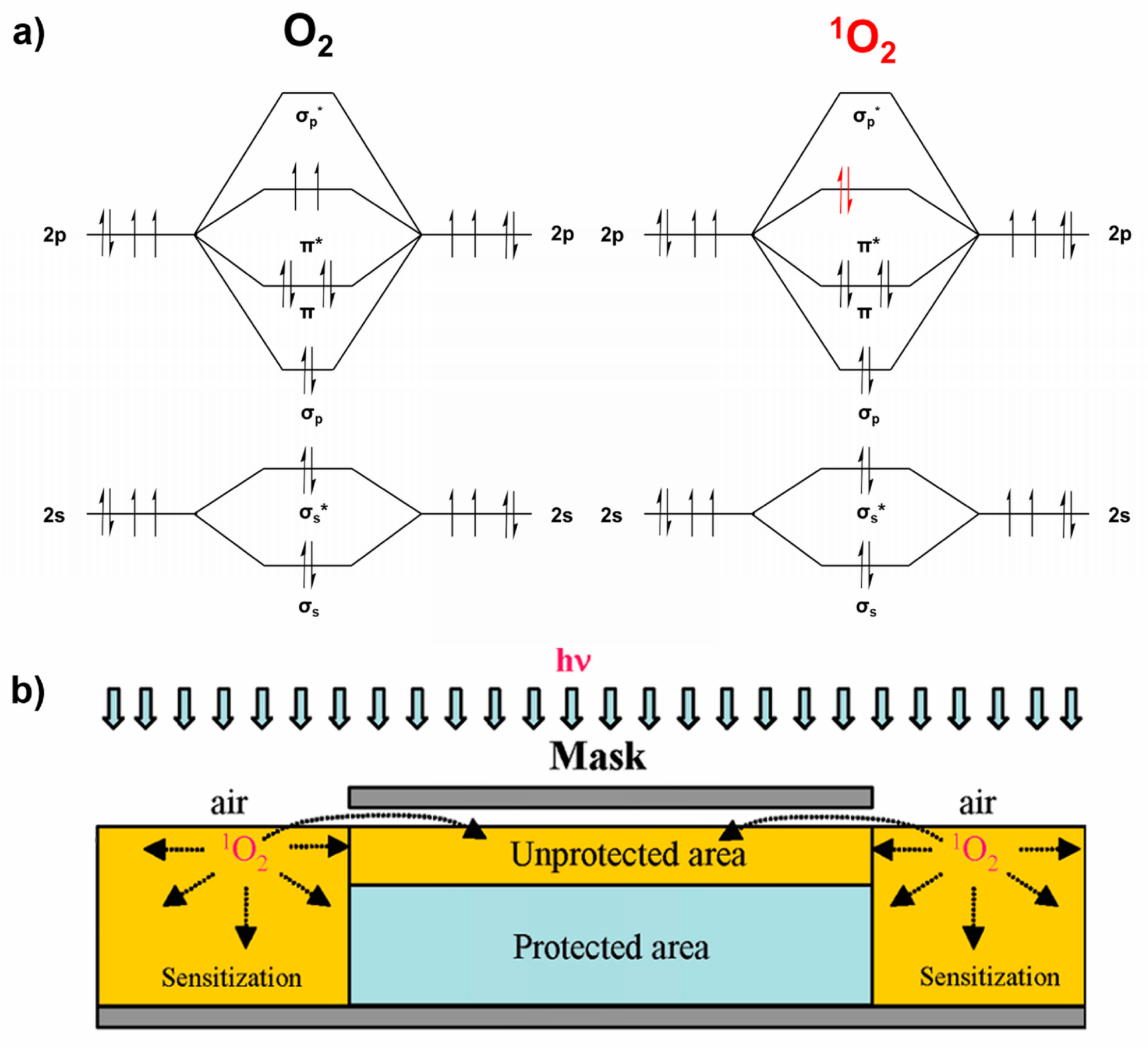
Singlet oxygen, O2(1Δg), the lowest excited electronic state of molecular oxygen (Figure 9a), has a characteristic chemistry which sets it apart from other reactive oxygen species. It can be prepared in several ways, including chemical reactions [59,60], but one of the most convenient ways involves electronic energy transfer from an excited state of a given molecule, a so-called sensitizer. This approach has great relevance for cell biology and biotechnology (e.g., cellular stress) as well as for medical applications (e.g., photodynamic therapy of tumors), and has been applied for the chemical patterning of surfaces. One of the first applications of singlet oxygen to photoimaging processes was reported in 1987 by D. S. Breslow et al., who described the use of singlet oxygen to develop a photosensitive lithographic plate. Zinc tetraphenylporphyrin was selected as the photosensitizer [61]. C. Carre et al. and, one year later in 1988, D. J. Lougnot et al. described processes for the recording of holograms produced by near-infrared emitting lasers, which involved the sensitization of singlet oxygen and oxidation of an adapted trap. Carre et al. used tricarbocyanine dyes as photosensitizers, while different dyes (thionine, methylene blue, eosin, rose Bengal, acridine orange) were chosen by Lougnot et al. [62].
Porphyrins and phthalocyanines are among the most versatile photosensitizers for the production of singlet oxygen [63]. They are a large family of pyrrole-based molecules with remarkable chemical and thermal stability. Owing to their large conjugated electron system, they display intense absorption bands in the visible range, a property which is shared by their metal complexes. The optical spectrum of porphyrins is characterized by a very strong absorption in the 400–450 nm region (Soret band, due to a π-π* transition) and in the 500–700 nm region (Q band) [64]. Porphyrin-based photocatalytic lithography was proposed by J. P Bearinger et al. in 2008 [65] as an alternative approach to photocatalytic oxide-based lithographic approaches. Suitable photosensitizers, such as copper chlorophyllin, hematoporphyrin IX, and magnesium phthalocyanine, were applied from their solutions on the surface of a patterned stamp mask made of poly(dimethyl siloxane) (PDMS). PDMS was chosen as a convenient stamp matrix for its transparency, flexibility, and chemical inertness. In this approach, the stamp is a mask, not in the sense of blocking light exposure to certain regions of the substrate, but rather in the sense of localizing chemical reactivity to the areas of contact between the stamp and the surface to be patterned. In other words, in contrast to usual stamping or contact printing, mass is not transferred from the stamp to the substrate.
This technique is independent from the chemistry of the substrate and allowed to perform quick (on a timescale of seconds) chemical patterning of substrates at the micrometer and sub-micrometer scale. Efficient excitation of the photocatalyst could be achieved with low-power sources, such as 480 nm (blue) or 660 nm (red) light from light-emitting diodes (LEDs). Applications of porphyrin-based photocatalytic lithography have been reported for the patterning of self-assembled monolayers and of polymers (such as an oxidation-sensitive poly(propylene sulfide)-poly(ethylene glycol) (PPS-b-PEG) block copolymer) [66].
It is noteworthy to compare the photocatalytic activity of oxide semiconductors with that of porphyrin-based sensitizers. In titanium dioxide, electron-hole pairs are generated upon excitation with light of the proper wavelength, and may migrate ~75 nm from their source in a free field region. They subsequently migrate and split, the holes diffusing to the surface, where they produce •OH and H2O2 by interacting with adsorbed oxygen and water molecules. These intermediate steps of electron-hole pair production, splitting and diffusion, are absent for excited photosensitizers such as porphyrins. However, the lifetime of hole-generated hydroxyl radicals and hydrogen peroxide is considerably higher than that of singlet oxygen—the latter is in the order of 10–40 ns, corresponding to a maximum diffusion distance of 10–20 nm. The possibility of generating features as small as 50 nm has been postulated, assuming that proper mechanics are devised to position porphyrin-bearing photomasks on surfaces and sufficiently constrained species migration [67].
These considerations can be extended to another kind of singlet oxygen sensitizer, namely anthracene derivatives, whose patterning applications have been described by W. Fudickar and T. Linker [68,69]. In these works, the photoreaction between anthracenes and singlet oxygen was demonstrated for applications, either as a photoswitch or as a photoresist (Figure 9b).
6. Conclusions
Photocatalytic lithography is a powerful enabling approach for the micro- and nanopatterning of surfaces. It is solvent-free, cost-effective, scalable, easy-to-use, compatible with current fabrication techniques, and it enables the design of a variety of structures. The versatility of photocatalytic lithography has been demonstrated for applications as diverse as the generation of superhydrophilic–superhydrophobic patterns, the patterning of polymer brushes, the sculpturing of metal nanoparticles, and the modification of graphene. All these results point out not only what has been done but also suggest new research directions. Improved photocatalysts may allow to reduce the exposure time, increase the resolution, and even to use visible light instead of UV light. The patterning of mussel-inspired, and in general of bio(macro)molecules-derived, coatings is worthy of investigation, as well as the development of self-cleaning, recyclable SERS-based sensing platforms. Eventually, the use of gas-phase, photocatalyst-promoted reactions may open new avenues for surface functionalization [70]. Given all these opportunities, it is reasonable to expect that photocatalytic lithography will become increasingly popular over time.
Author Contributions
The authors contributed equally to this work.
Funding
This research received no external funding.
Acknowledgments
G.P. would like to express his gratitude to colleagues and friends for their help and generous support over many years. Especially due are the acknowledgments to: Laura Meda, Gianluigi Marra, Alberto Savoini and Mario Salvalaggio from the Eni Donegani Research Centre for Renewable Energies and the Environment (Novara, Italy), Matthias Dübner from ETH (Zürich, Switzerland), Celestino Padeste from PSI (Villigen, Switzerland), Matthias Griesser from Montanuniversität (Leoben, Austria), Silvia Ardizzone from Università di Milano (Milano, Italy) and, last but not least, Katia Sparnacci from Università del Piemonte Orientale (Alessandria, Italy).
Conflicts of Interest
The authors declare no conflict of interest.
References
- Griffiths, A. Prints and Printmaking: An Introduction to the History and Techniques, 2nd ed.; University of California Press: Berkeley, CA, USA, 1996; ISBN 978-0-52020-714-1. [Google Scholar]
- Xia, Y.; Rogers, J.A.; Paul, K.E.; Whitesides, G.M. Unconventional Methods for Fabricating and Patterning Nanostructures. Chem. Rev. 1999, 99, 1823–1848. [Google Scholar] [CrossRef] [PubMed]
- Qin, D.; Xia, Y.; Whitesides, G.M. Soft lithography for micro- and nanoscale patterning. Nat. Protoc. 2010, 5, 491–502. [Google Scholar] [CrossRef] [PubMed] [Green Version]
- Carp, O.; Huisman, C.L.; Reller, A. Photoinduced reactivity of titanium dioxide. Prog. Solid State Chem. 2004, 32, 33–177. [Google Scholar] [CrossRef]
- Fujishima, A.; Zhang, X.; Tryk, D. TiO2 photocatalysis and related surface phenomena. Surf. Sci. Rep. 2008, 63, 515–582. [Google Scholar] [CrossRef]
- Fujishima, A.; Honda, K. Electrochemical photolysis of water at a semiconductor electrode. Nature 1972, 238, 37–38. [Google Scholar] [CrossRef] [PubMed]
- Linsebigler, A.L.; Lu, G.; Yates, J.T. Photocatalysis on TiO2 Surfaces: Principles, Mechanisms, and Selected Results. Chem. Rev. 1995, 95, 735–758. [Google Scholar] [CrossRef]
- Chen, X.; Selloni, A. Introduction: Titanium Dioxide (TiO2) Nanomaterials. Chem. Rev. 2014, 114, 9281–9282. [Google Scholar] [CrossRef] [PubMed]
- Kubo, W.; Tatsuma, T. Mechanisms of photocatalytic remote oxidation. J. Am. Chem. Soc. 2006, 128, 16034–16035. [Google Scholar] [CrossRef]
- Kubo, W.; Tatsuma, T. Conversion of a solid surface from super-hydrophobic to super-hydrophilic by photocatalytic remote oxidation and photocatalytic lithography. Appl. Surf. Sci. 2005, 243, 125–128. [Google Scholar] [CrossRef]
- Ganter, P.; Lotsch, B.V. Photocatalytic Nanosheet Lithography: Photolithography based on Organically Modified Photoactive 2D Nanosheets. Angew. Chem. Int. Ed. 2017, 56, 8389–8392. [Google Scholar] [CrossRef] [Green Version]
- Tatsuma, T.; Tachibana, S.; Miwa, T.; Tryk, D.A.; Fujishima, A. Remote Bleaching of Methylene Blue by UV-Irradiated TiO2 in the Gas Phase. J. Phys. Chem. B 1999, 103, 8033–8035. [Google Scholar] [CrossRef]
- Tatsuma, T.; Kubo, W.; Fujishima, A. Patterning of solid surfaces by photocatalytic lithography based on the remote oxidation effect of TiO2. Langmuir 2002, 18, 9632–9634. [Google Scholar] [CrossRef]
- Spori, D.M.; Venkataraman, N.V.; Tosatti, S.G.P.; Durmaz, F.; Spencer, N.D.; Zürcher, S. Influence of alkyl chain length on phosphate self-assembled monolayers. Langmuir 2007, 23, 8053–8060. [Google Scholar] [CrossRef] [PubMed]
- Paz, Y. Self-assembled monolayers and titanium dioxide: From surface patterning to potential applications. Beilstein J. Nanotechnol. 2011, 2, 845–861. [Google Scholar] [CrossRef] [PubMed] [Green Version]
- Guo, M.Y.; Ng, A.M.C.; Liu, F.; Djurišić, A.B.; Chan, W.K. Photocatalytic activity of metal oxides-The role of holes and OH• radicals. Appl. Catal. B Environ. 2011, 107, 150–157. [Google Scholar] [CrossRef]
- Degawa, R.; Wang, P.; Tanaka, D.; Park, S.; Sakai, N.; Tatsuma, T.; Okamoto, K.; Tamada, K. Colorimetric Detection of an Airborne Remote Photocatalytic Reaction Using a Stratified Ag Nanoparticle Sheet. Langmuir 2016, 32, 8154–8162. [Google Scholar] [CrossRef]
- Kondrakov, A.O.; Ignatev, A.N.; Lunin, V.V.; Frimmel, F.H.; Bräse, S.; Horn, H. Roles of water and dissolved oxygen in photocatalytic generation of free OH radicals in aqueous TiO2 suspensions: An isotope labeling study. Appl. Catal. B Environ. 2016, 182, 424–430. [Google Scholar] [CrossRef]
- Kubo, W.; Tatsuma, T. Photocatalytic remote oxidation with various photocatalysts and enhancement of its activity. J. Mater. Chem. 2005, 15, 3104. [Google Scholar] [CrossRef]
- Smith, R.K.; Lewis, P.A.; Weiss, P.S. Patterning self-assembled monolayers. Prog. Surf. Sci. 2004, 75, 1–68. [Google Scholar] [CrossRef]
- Kubo, W.; Tatsuma, T.; Fujishima, A.; Kobayashi, H. Mechanisms and Resolution of Photocatalytic Lithography. J. Phys. Chem. B 2004, 108, 3005–3009. [Google Scholar] [CrossRef]
- Tatsuma, T.; Tachibana, S.; Fujishima, A. Remote oxidation of organic compounds by UV-irradiated TiO2 via the gas phase. J. Phys. Chem. 2001, 105, 6987–6992. [Google Scholar] [CrossRef]
- Tizazu, G.; El-Zubir, O.; Brueck, S.R.J.; Lidzey, D.G.; Leggett, G.J.; Lopez, G.P. Large area nanopatterning of alkylphosphonate self-assembled monolayers on titanium oxide surfaces by interferometric lithography. Nanoscale 2011, 3, 2511. [Google Scholar] [CrossRef] [PubMed]
- Nakata, K.; Nishimoto, S.; Kubo, A.; Tryk, D.; Ochiai, T.; Murakami, T.; Fujishima, A. Fabrication and application of TiO2-based superhydrophilic- superhydrophobic patterns on titanium substrates for offset printing. Chem. Asian J. 2009, 4, 984–988. [Google Scholar] [CrossRef] [PubMed]
- Nishimoto, S.; Kubo, A.; Nohara, K.; Zhang, X.; Taneichi, N.; Okui, T.; Liu, Z.; Nakata, K.; Sakai, H.; Murakami, T.; et al. TiO2-based superhydrophobic-superhydrophilic patterns: Fabrication via an ink-jet technique and application in offset printing. Appl. Surf. Sci. 2009, 255, 6221–6225. [Google Scholar] [CrossRef]
- Blondiaux, N.; Zürcher, S.; Liley, M.; Spencer, N.D. Fabrication of multiscale surface-chemical gradients by means of photocatalytic lithography. Langmuir 2007, 23, 3489–3494. [Google Scholar] [CrossRef]
- Lee, J.P.; Sung, M.M. A New Patterning Method Using Photocatalytic Lithography and Selective Atomic Layer Deposition. J. Am. Chem. Soc. 2004, 126, 28–29. [Google Scholar] [CrossRef]
- Tatsuma, T.; Yoshida, Y.; Shitanda, I.; Notsu, H. Algal biosensor array on a single electrode. Analyst 2009, 134, 223–225. [Google Scholar] [CrossRef] [PubMed]
- Komori, K.; Nada, J.; Nishikawa, M.; Notsu, H.; Tatsuma, T.; Sakai, Y. Simultaneous evaluation of toxicities using a mammalian cell array chip prepared by photocatalytic lithography. Anal. Chim. Acta 2009, 653, 222–227. [Google Scholar] [CrossRef]
- Panzarasa, G. The art and science of polymer brushes: Recent developments in patterning and characterization approaches. Chimia 2017, 71, 354–358. [Google Scholar] [CrossRef]
- Panzarasa, G.; Aghion, S.; Soliveri, G.; Consolati, G.; Ferragut, R. Positron annihilation spectroscopy: A new frontier for understanding nanoparticle- loaded polymer brushes. Nanotechnology 2016, 27, 02LT03. [Google Scholar] [CrossRef]
- Panzarasa, G.; Aghion, S.; Marra, G.; Wagner, A.; Liedke, M.O.; Elsayed, M.; Krause-Rehberg, R.; Ferragut, R.; Consolati, G. Probing the Impact of the Initiator Layer on Grafted-from Polymer Brushes: A Positron Annihilation Spectroscopy Study. Macromolecules 2017, 50, 5574–5581. [Google Scholar] [CrossRef]
- Panzarasa, G.; Dübner, M.; Pifferi, V.; Soliveri, G.; Padeste, C. ON/OFF switching of silicon wafer electrochemistry by pH-responsive polymer brushes. J. Mater. Chem. C 2016, 4, 6287–6294. [Google Scholar] [CrossRef] [Green Version]
- Panzarasa, G.; Pifferi, V. On the capacitive behavior of silicon electrodes modified with ultrathin hydrophobic polymer brushes. J. Solid State Electrochem. 2018, 4, 1269–1273. [Google Scholar] [CrossRef]
- Dehghani, E.S.; Aghion, S.; Anwand, W.; Consolati, G.; Ferragut, R.; Panzarasa, G. Investigating the structure of crosslinked polymer brushes (brush-gels) by means of Positron Annihilation Spectroscopy. Eur. Polym. J. 2018, 99, 415–421. [Google Scholar] [CrossRef]
- Braunecker, W.A.; Matyjaszewski, K. Controlled/living radical polymerization: Features, developments, and perspectives. Prog. Polym. Sci. 2007, 32, 93–146. [Google Scholar] [CrossRef]
- Matyjaszewski, K.; Dong, H.; Jakubowski, W.; Pietrasik, J.; Kusumo, A. Grafting from Surfaces for “Everyone”: ARGET ATRP in the Presence of Air. Langmuir 2007, 23, 4528–4531. [Google Scholar] [CrossRef]
- Yu, Q.; Ista, L.K.; Gu, R.; Zauscher, S.; López, G.P. Nanopatterned polymer brushes: Conformation, fabrication and applications. Nanoscale 2016, 8, 680–700. [Google Scholar] [CrossRef]
- Panzarasa, G.; Soliveri, G.; Sparnacci, K.; Ardizzone, S.; Information, S. Patterning of polymer brushes made easy using titanium dioxide: Direct and remote photocatalytic lithography. Chem. Commun. 2015, 51, 7313–7316. [Google Scholar] [CrossRef] [PubMed]
- Panzarasa, G.; Soliveri, G.; Ardizzone, S.; Sparnacci, K. Photocatalytic lithography: An innovative approach to obtain patterned pH-responsive polymer brushes. Mater. Today Proc. 2015, 2, 4183–4189. [Google Scholar] [CrossRef]
- Maino, G.; Meroni, D.; Pifferi, V.; Falciola, L.; Soliveri, G.; Cappelletti, G.; Ardizzone, S. Electrochemically assisted deposition of transparent, mechanically robust TiO2 films for advanced applications. J. Nanopart. Res. 2013, 15, 2087. [Google Scholar] [CrossRef]
- Panzarasa, G.; Soliveri, G.; Ardizzone, S. Crafting positive/negative patterns and nanopillars of polymer brushes by photocatalytic lithography. Colloids Surf. A Physicochem. Eng. Asp. 2016, 506, 833–839. [Google Scholar] [CrossRef] [Green Version]
- Panzarasa, G.; Soliveri, G.; Pifferi, V. Tuning the electrochemical properties of silicon wafer by grafted-from micropatterned polymer brushes. J. Mater. Chem. C 2016, 4, 340–347. [Google Scholar] [CrossRef] [Green Version]
- Kettling, F.; Vonhören, B.; Krings, J.A.; Saito, S.; Ravoo, B.J. One-step synthesis of patterned polymer brushes by photocatalytic microcontact printing. Chem. Commun. 2015, 51, 1027–1030. [Google Scholar] [CrossRef] [PubMed] [Green Version]
- Panzarasa, G.; Dübner, M.; Soliveri, G.; Edler, M.; Griesser, T. Branched poly(ethyleneimine): A versatile scaffold for patterning polymer brushes by means of remote photocatalytic lithography. Nanotechnology 2017, 28, 395302. [Google Scholar] [CrossRef]
- Wenderich, K.; Mul, G. Methods, Mechanism, and Applications of Photodeposition in Photocatalysis: A Review. Chem. Rev. 2016, 116, 14587–14619. [Google Scholar] [CrossRef]
- Dibbell, R.S.; Soja, G.R.; Hoth, R.M.; Watson, D.F. Photocatalytic patterning of monolayers for the site-selective deposition of quantum dots onto TiO2 surfaces. Langmuir 2007, 23, 3432–3439. [Google Scholar] [CrossRef] [PubMed]
- Panzarasa, G. Just What Is It That Makes Silver Nanoprisms so Different, so Appealing? J. Chem. Educ. 2015, 92, 1918–1923. [Google Scholar] [CrossRef]
- Panzarasa, G.; Soliveri, G.; Marra, G.; Meda, L.; Savoini, A.; Ardizzone, S.; Salvalaggio, M. Sculpturing patterns of plasmonic silver nanoprisms by means of photocatalytic lithography. Nanotechnology 2017, 28, 155302. [Google Scholar] [CrossRef] [PubMed]
- Geim, A.K.; MacDonald, A.H. Graphene: Exploring carbon flatland. Phys. Today 2007, 60, 35–41. [Google Scholar] [CrossRef] [Green Version]
- Bonaccorso, F.; Sun, Z.; Hasan, T.; Ferrari, A.C. Graphene photonics and optoelectronics. Nat. Photonics 2010, 4, 611–622. [Google Scholar] [CrossRef] [Green Version]
- Castro Neto, A.H.; Guinea, F.; Peres, N.M.R.; Novoselov, K.S.; Geim, A.K. The electronic properties of graphene. Rev. Mod. Phys. 2009, 81, 109–162. [Google Scholar] [CrossRef] [Green Version]
- Panzarasa, G.; Consolati, G.; Scavini, M.; Longhi, M.; Quasso, F. Convenient Preparation of Graphene Oxide from Expandable Graphite and Its Characterization by Positron Annihilation Lifetime Spectroscopy. C 2019, 5, 6. [Google Scholar] [CrossRef]
- Yao, H.-B.; Wu, L.-H.; Cui, C.-H.; Fang, H.-Y.; Yu, S.-H. Direct fabrication of photoconductive patterns on LBL assembled graphene oxide/PDDA/titania hybrid films by photothermal and photocatalytic reduction. J. Mater. Chem. 2010, 20, 5190. [Google Scholar] [CrossRef]
- Zhang, L.; Diao, S.; Nie, Y.; Yan, K.; Liu, N.; Dai, B.; Xie, Q.; Reina, A.; Kong, J.; Liu, Z. Photocatalytic patterning and modification of graphene. J. Am. Chem. Soc. 2011, 133, 2706–2713. [Google Scholar] [CrossRef]
- Radich, J.G.; Krenselewski, A.L.; Zhu, J.; Kamat, P.V. Is Graphene a Stable Platform for Photocatalysis? Mineralization of Reduced Graphene Oxide with UV-Irradiated TiO2 Nanoparticles. Chem. Mater. 2014, 26, 4662–4668. [Google Scholar] [CrossRef]
- Mun, D.-H.; Lee, H.J.; Bae, S.; Kim, T.-W.; Lee, S.H. Photocatalytic decomposition of graphene over a ZnO surface under UV irradiation. Phys. Chem. Chem. Phys. 2015, 17, 15683–15686. [Google Scholar] [CrossRef]
- Kapitanova, O.O.; Panin, G.N.; Cho, H.D.; Baranov, A.N.; Kang, T.W. Formation of self-assembled nanoscale graphene/graphene oxide photomemristive heterojunctions using photocatalytic oxidation. Nanotechnology 2017, 28, 204005. [Google Scholar] [CrossRef] [PubMed]
- Panzarasa, G.; Sparnacci, K. Glowing teacup demonstration: Trautz-schorigin reaction of natural polyphenols. J. Chem. Educ. 2012, 89, 1297–1300. [Google Scholar] [CrossRef]
- Panzarasa, G. Just Add Luminol to Turn the Spotlight on Radziszewski Amidation. ACS Omega 2018, 3, 13179–13182. [Google Scholar] [CrossRef]
- Breslow, D.S.; Simpson, D.A.; Kramer, B.D.; Schwarz, R.J.; Newburg, N.R. A new photoimaging system based on singlet oxygen. Ind. Eng. Chem. 1987, 10, 2144–2148. [Google Scholar] [CrossRef]
- Lougnot, D.J.; Ritzenthaler, D.; Carre, C.; Fouassier, J.P. A new gated system for two-photon holographic recording in the near infrared. J. Appl. Phys. 1988, 63, 4841–4848. [Google Scholar] [CrossRef]
- Kimel, S.; Tromberg, B.J.; Roberts, W.G.; Berns, M.W. Singlet oxygen generation of porphyrins, chlorins, and phthalocyanines. J. Photochem. Photobiol. 1989, 50, 175–183. [Google Scholar] [CrossRef]
- Suslick, K.S.; Rakow, N.A.; Kosal, M.E.; Chou, J.H. The materials chemistry of porphyrins and metalloporphyrins. J. Porphyr. Phthalocyanines 2000, 4, 407–413. [Google Scholar] [CrossRef] [Green Version]
- Bearinger, J.P.; Stone, G.; Christian, A.T.; Dugan, L.; Hiddessen, A.L.; Wu, K.J.J.; Wu, L.; Hamilton, J.; Stockton, C.; Hubbell, J.A. Porphyrin-based photocatalytic lithography. Langmuir 2008, 24, 5179–5184. [Google Scholar] [CrossRef]
- Bearinger, J.P.; Stone, G.; Hiddessen, A.L.; Dugan, L.C.; Wu, L.; Hailey, P.; Conway, J.W.; Kuenzler, T.; Feller, L.; Cerritelli, S.; et al. Phototocatalytic lithography of poly(propylene sulfide) block copolymers: Toward high-throughput nanolithography for biomolecular arraying applications. Langmuir 2009, 25, 1238–1244. [Google Scholar] [CrossRef]
- Bearinger, J.P.; Stone, G.; Dugan, L.C.; El Dasher, B.; Stockton, C.; Conway, J.W.; Kuenzler, T.; Hubbell, J. a Porphyrin-based photocatalytic nanolithography: A new fabrication tool for protein arrays. Mol. Cell. Proteomics 2009, 8, 1823–1831. [Google Scholar] [CrossRef]
- Fudickar, W.; Linker, T. Photoimaging with singlet oxygen at the solid-air interface. Langmuir 2009, 25, 9797–9803. [Google Scholar] [CrossRef]
- Fudickar, W.; Linker, T. Novel anthracene materials for applications in lithography and reversible photoswitching by light and air. Langmuir 2010, 26, 4421–4428. [Google Scholar] [CrossRef] [PubMed]
- Griesser, T.; Montanuniversität, Leoben, Austria. Personal communication, 2016.
Figure 1.
Primary steps in the mechanism of photocatalysis: (1) formation of charge carriers by photon absorption; (2) charge carrier recombination; (3) trapping of a conduction-band electron at a Ti(IV) site to yield Ti(III); (4) trapping of a valence-band hole at a superficial Ti–OH group; (5) initiation of an oxidative pathway by a valence-band hole; (6) initiation of a reductive pathway by a conduction-band electron; (7) further thermal (e.g., hydrolysis or active oxygen species-mediated reactions) and photocatalytic reactions to yield mineralization products. Adapted with permission from [8], American Chemical Society, 2014.
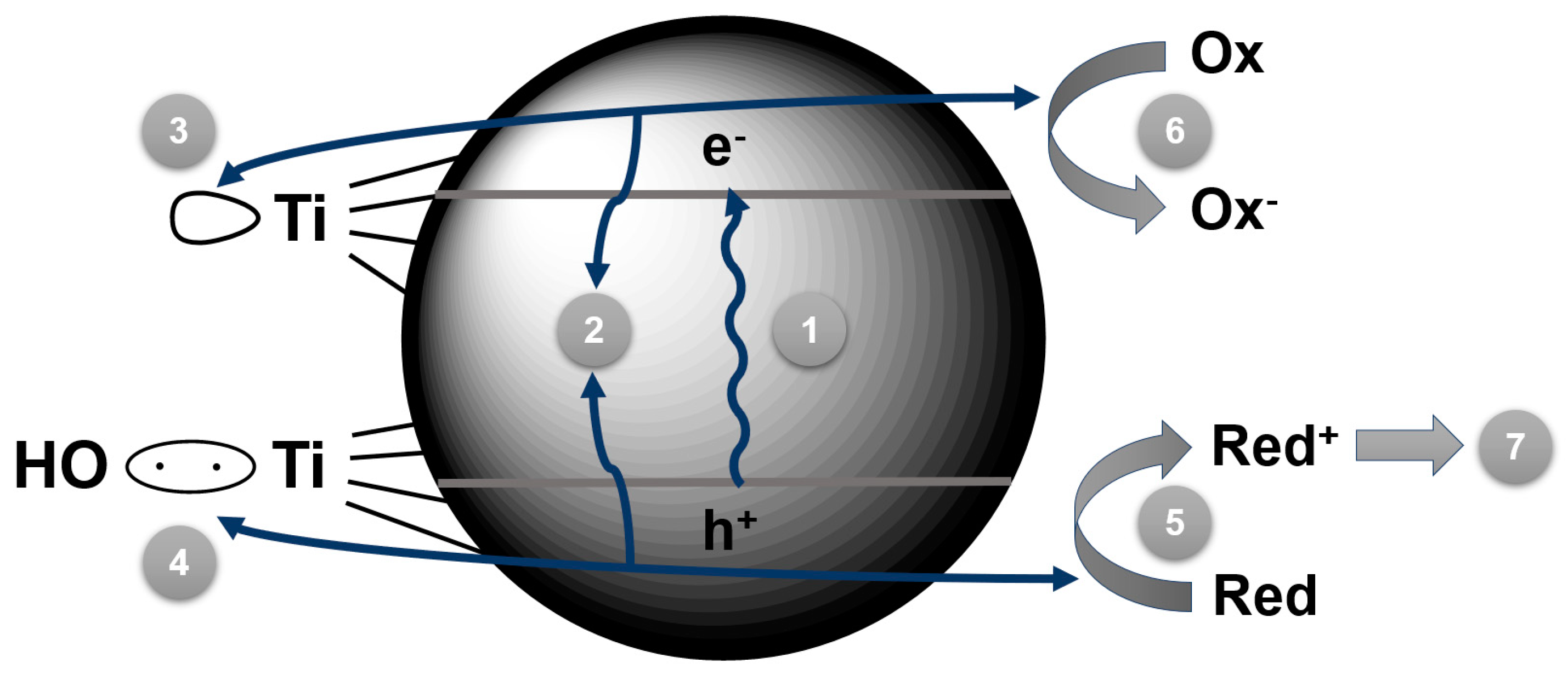
Figure 2.
Schematic representation of direct (a) and remote (b) photocatalytic lithography for the patterning of a self-assembled monolayer (SAM). The photocatalytically-generated reactive oxygen species responsible for the patterning are represented as red stars. Adapted with permission from [15], Beilstein-Institut for the Advancement of Chemical Sciences, 2011.
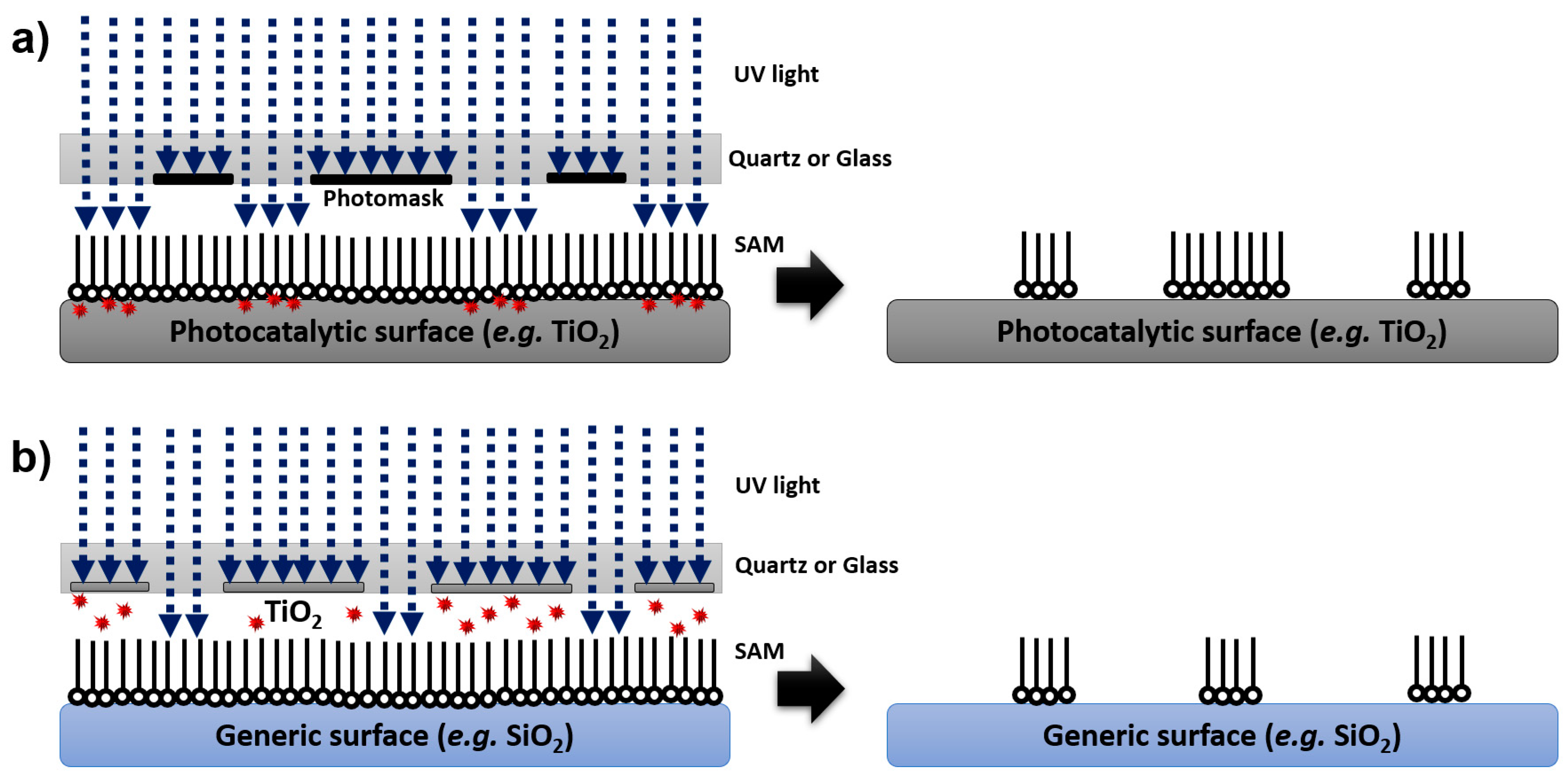
Figure 3.
Schematic representation of (a) polymer brushes obtained by surface-initiated polymerization and (b) the process to obtain patterned polymer brushes. The yellow spheres represent a surface-anchoring functional group for the initiator (red spheres) and the blue spheres the monomer(s). If the polymerization is controlled, the polymer chains are capped with an initiation site.
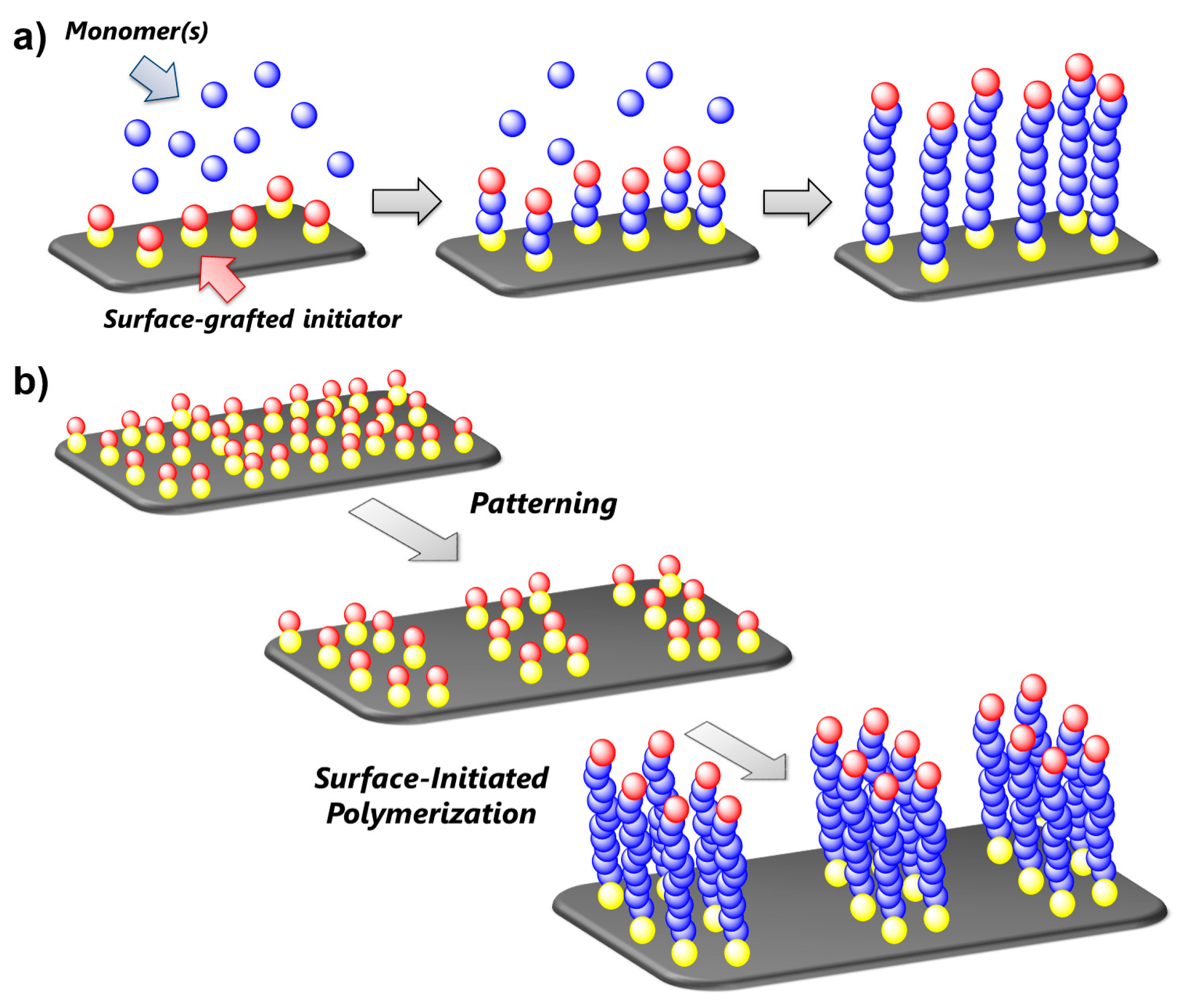
Figure 4.
Positive and negative patterns of polymer brushes obtained by direct photocatalytic lithography: (a) schematic representation of the experimental procedures; (b) Atomic force microscopy (AFM) images of the corresponding positive and negative patterns of polymer brushes. Reproduced with permission from [42], Wiley, 2016.

Figure 5.
Patterns of polymer brushes obtained by (a–f) direct and (g–i) remote photocatalytic lithography. Reproduced by permission of The Royal Society of Chemistry from ref. [39].
Figure 5.
Patterns of polymer brushes obtained by (a–f) direct and (g–i) remote photocatalytic lithography. Reproduced by permission of The Royal Society of Chemistry from ref. [39].
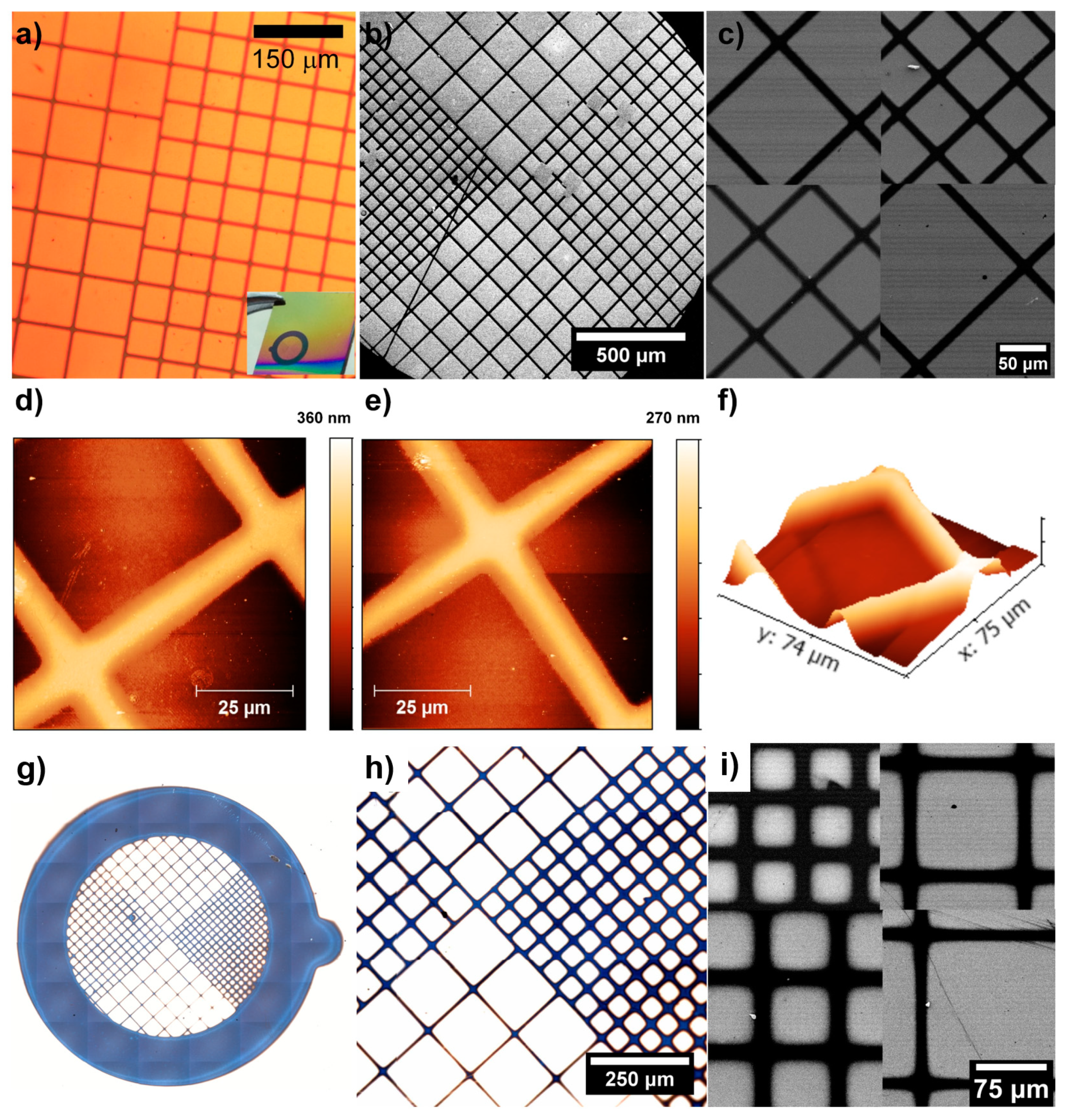
Figure 6.
Patterned polymer brushes obtained by remote photocatalytic colloidal lithography: (a) schematic representation of the process; (b,c) Scanning electron microscopy (SEM) images of the self-assembled colloidal mask and of the resulting polymer brushes pattern, respectively; (d,e) AFM and profile images of the polymer brushes pattern obtained. Reproduced with permission from [42], Wiley, 2016.
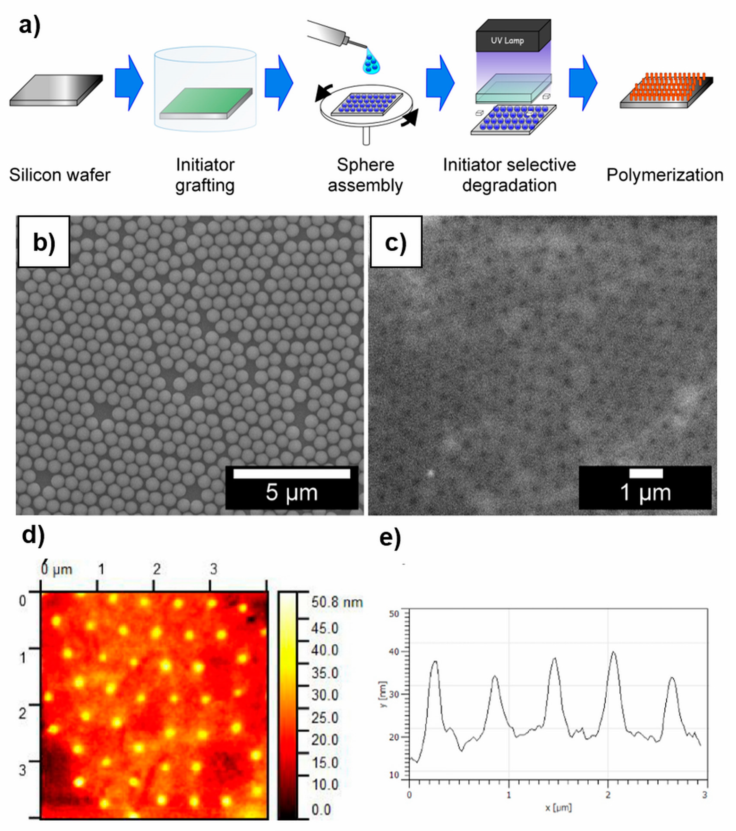
Figure 7.
Photocatalytic dissolution and reshaping of triangular silver nanoprisms self-assembled on titanium dioxide upon UV irradiation (a–c). The prisms are transformed into spheroids (d,e), which results in (f–i) patterns having different SERS behavior. Reproduced with permission from [49], IOP Publishing, 2017.
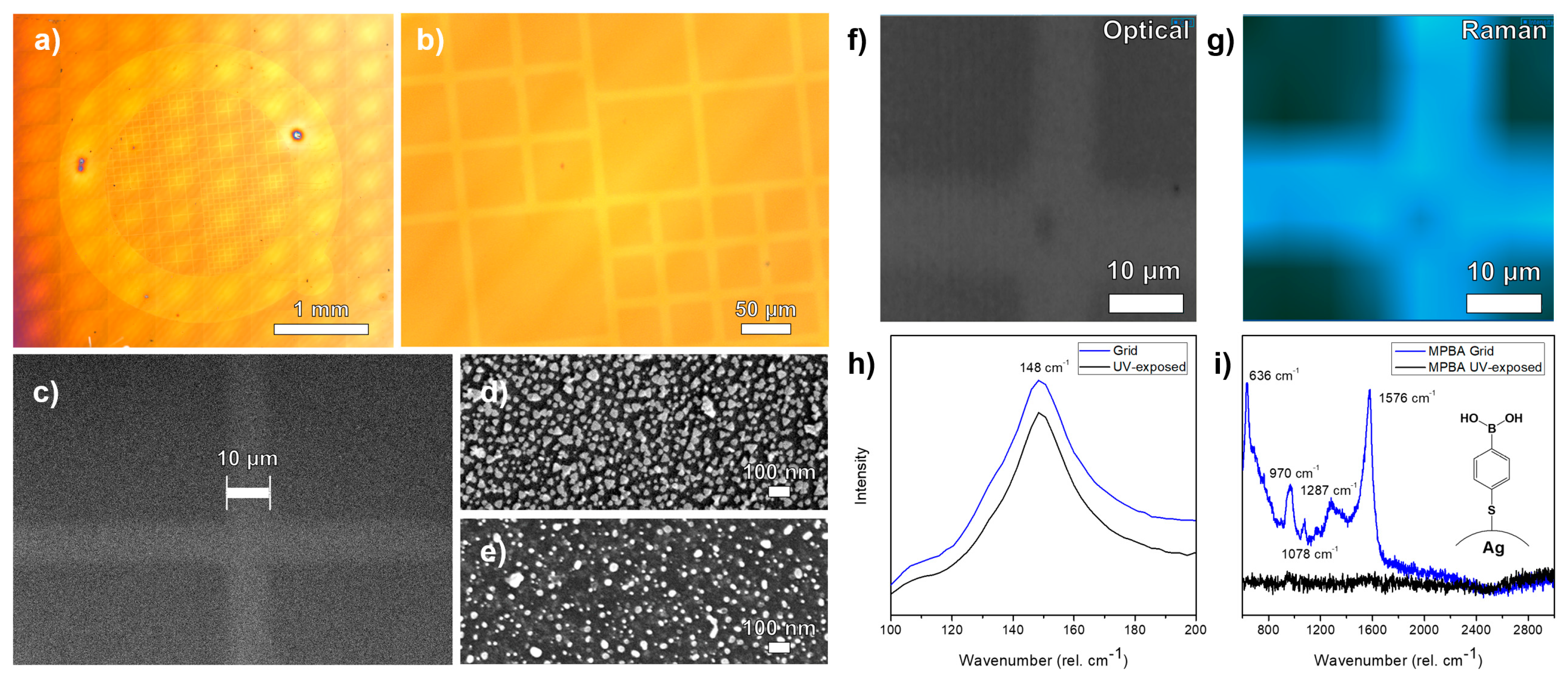
Figure 8.
Photocatalytic patterning of graphene. (a) Schematic illustration of the fabrication procedure of layer-by-layer hybrid films consisting of PDDA/GO/PDDA/TiOx. (b) Photographs of (PDDA/GO/PDDA/TiOx)n hybrid films with different layers, before and after illumination with a 300 W Xe lamp for 30 min. (c) Model setup for the photocatalytic reduction lithography (PRL) approach and the corresponding PRL patterns on the (PDDA/GO/PDDA/TiOx)20 hybrid film after illumination. Reproduced by permission of The Royal Society of Chemistry from ref. [54]. (d) Schematic illustration of the photocatalytic approach to engineering single- or few-layer graphene. (e,g) Optical and (f–i) SEM images of patterned reduced graphene oxide (RGO) illustrating the feasibility of complex structural design. Scale bars: (e–h) 50 μm, inset of (e) 100 μm, (i) 10 μm. Reproduced with permission from [55], American Chemical Society, 2011.
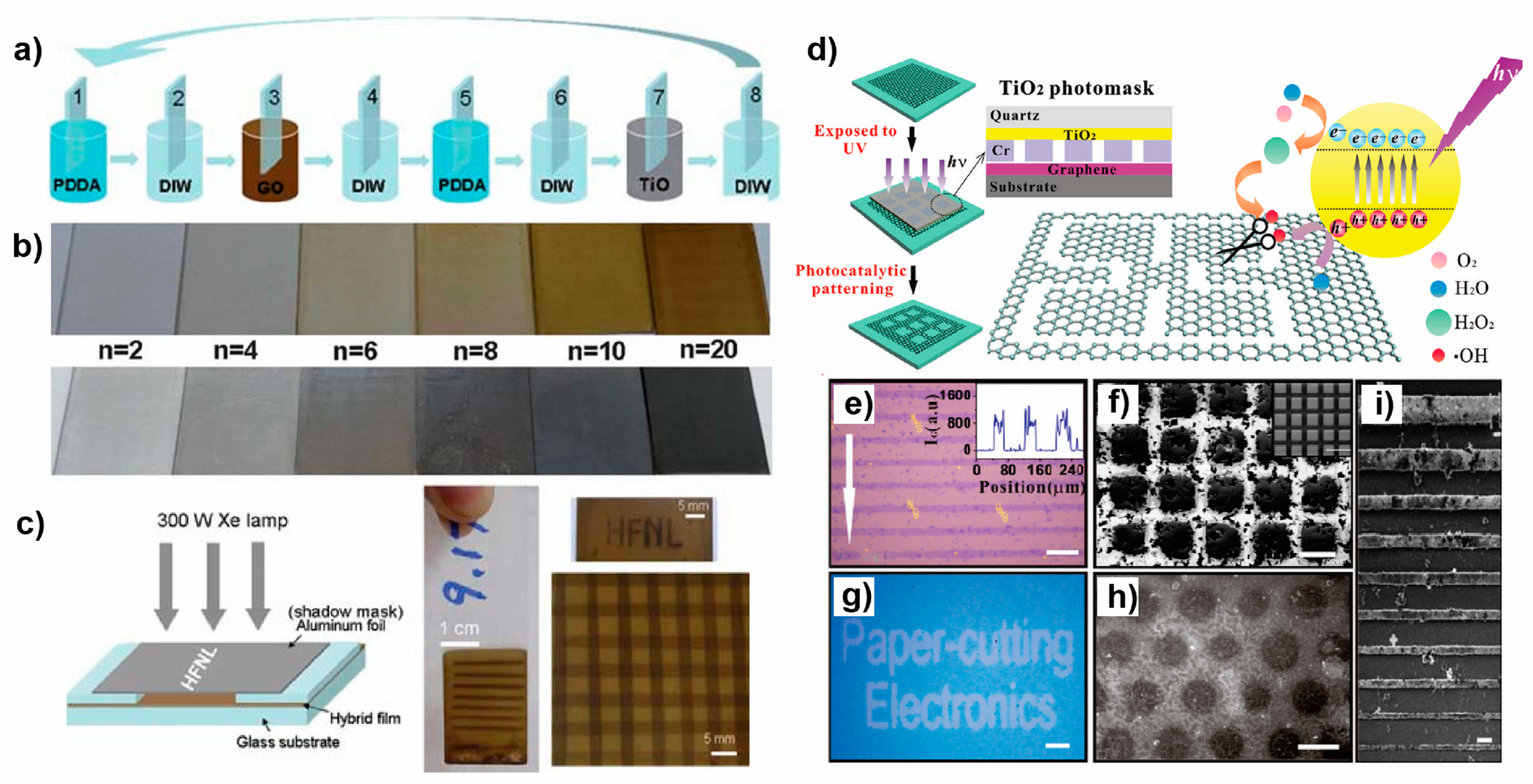
Figure 9.
(a) Molecular orbitals of triplet and singlet oxygen. (b) Schematic representation of singlet oxygen-mediated photocatalytic lithography. The reactive species is generated in correspondence with the exposed regions but can travel outside the sensitizer layer into the masked area. Reproduced with permission from [68], American Chemical Society, 2009.
© 2019 by the authors. Licensee MDPI, Basel, Switzerland. This article is an open access article distributed under the terms and conditions of the Creative Commons Attribution (CC BY) license (http://creativecommons.org/licenses/by/4.0/).
Share and Cite
MDPI and ACS Style
Panzarasa, G.; Soliveri, G. Photocatalytic Lithography. Appl. Sci. 2019, 9, 1266. https://doi.org/10.3390/app9071266
AMA Style
Panzarasa G, Soliveri G. Photocatalytic Lithography. Applied Sciences. 2019; 9(7):1266. https://doi.org/10.3390/app9071266
Chicago/Turabian StylePanzarasa, Guido, and Guido Soliveri. 2019. "Photocatalytic Lithography" Applied Sciences 9, no. 7: 1266. https://doi.org/10.3390/app9071266
Note that from the first issue of 2016, this journal uses article numbers instead of page numbers. See further details here.