


Design and Test of a Grain Cleaning Loss Monitoring Device for Wheat Combine Harvester

Abstract
1. Introduction
2. Materials and Methods
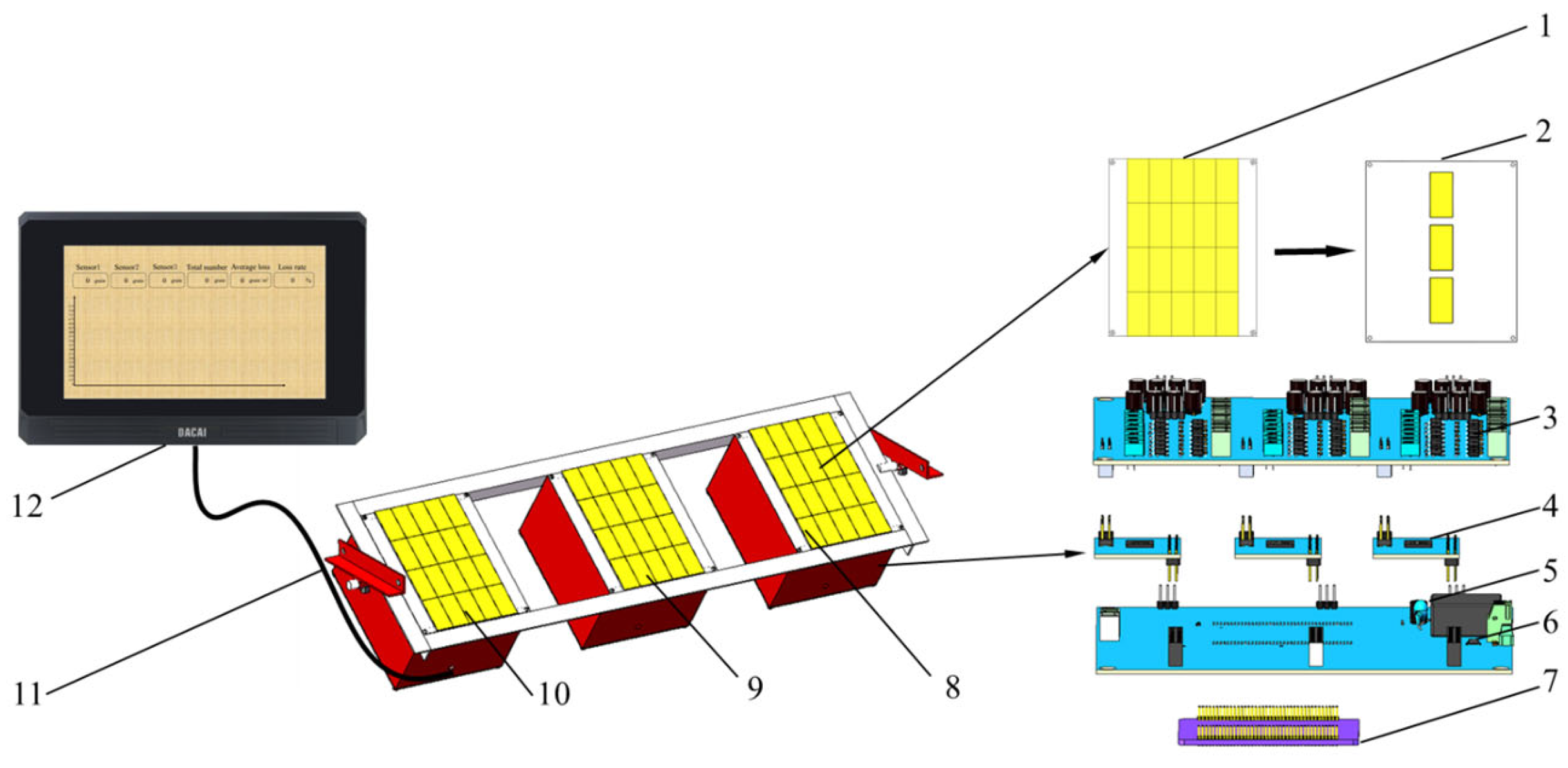
2.1. The Structure
2.2. Working Mechanism
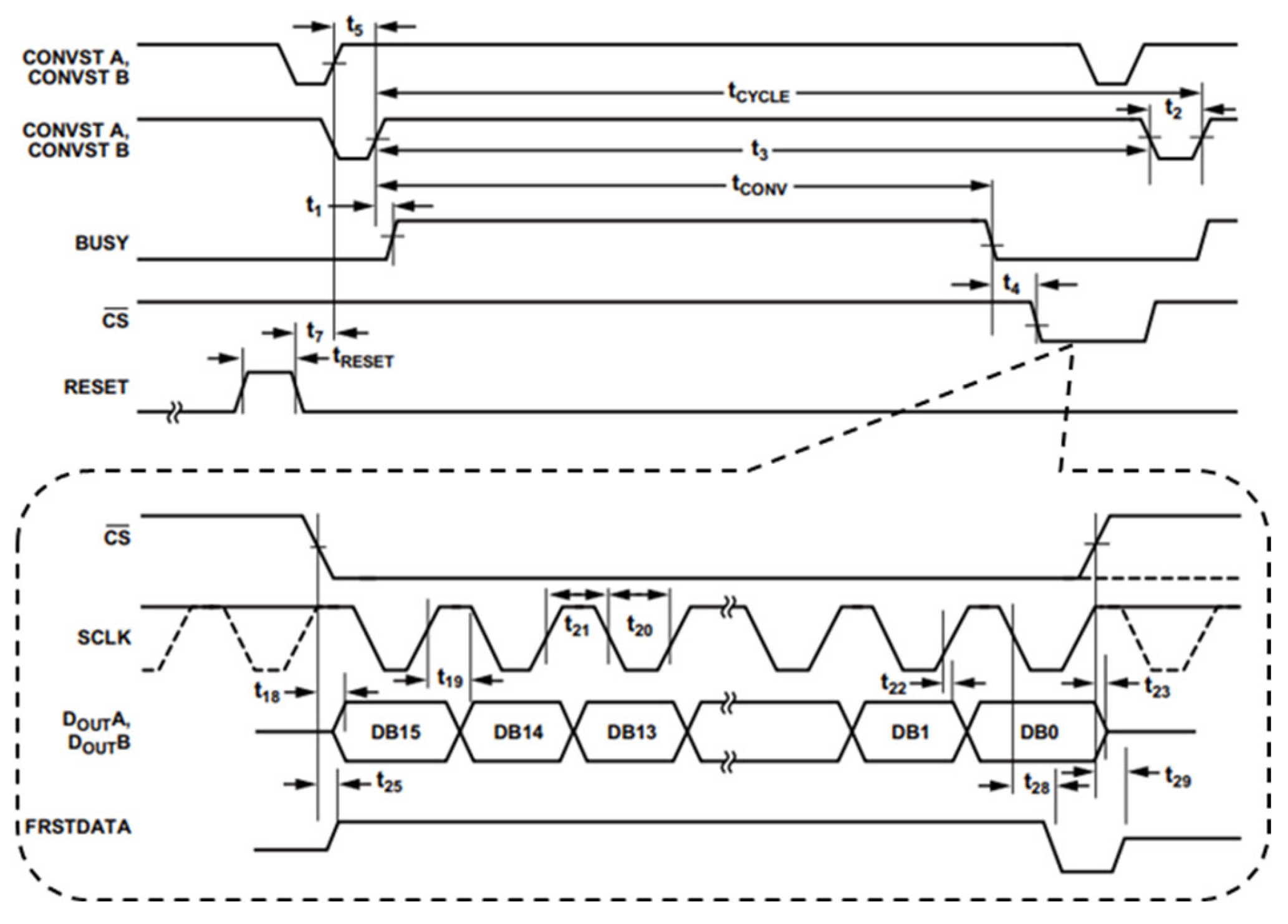
2.3. Hardware Circuit Design
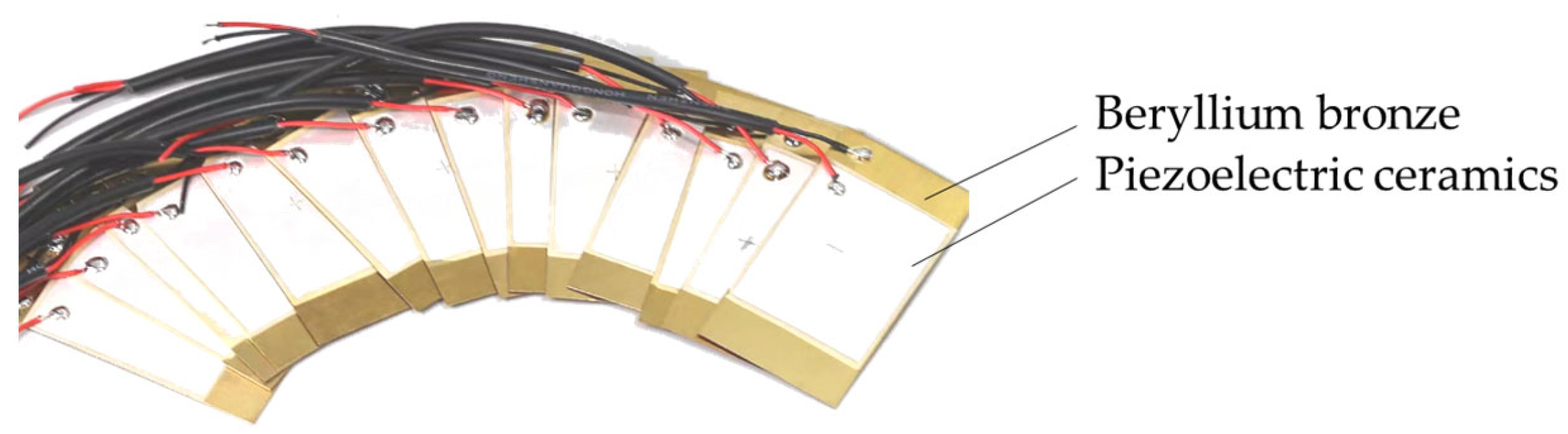
2.3.1. Design of a Bidirectional Array Piezoelectric Sensor
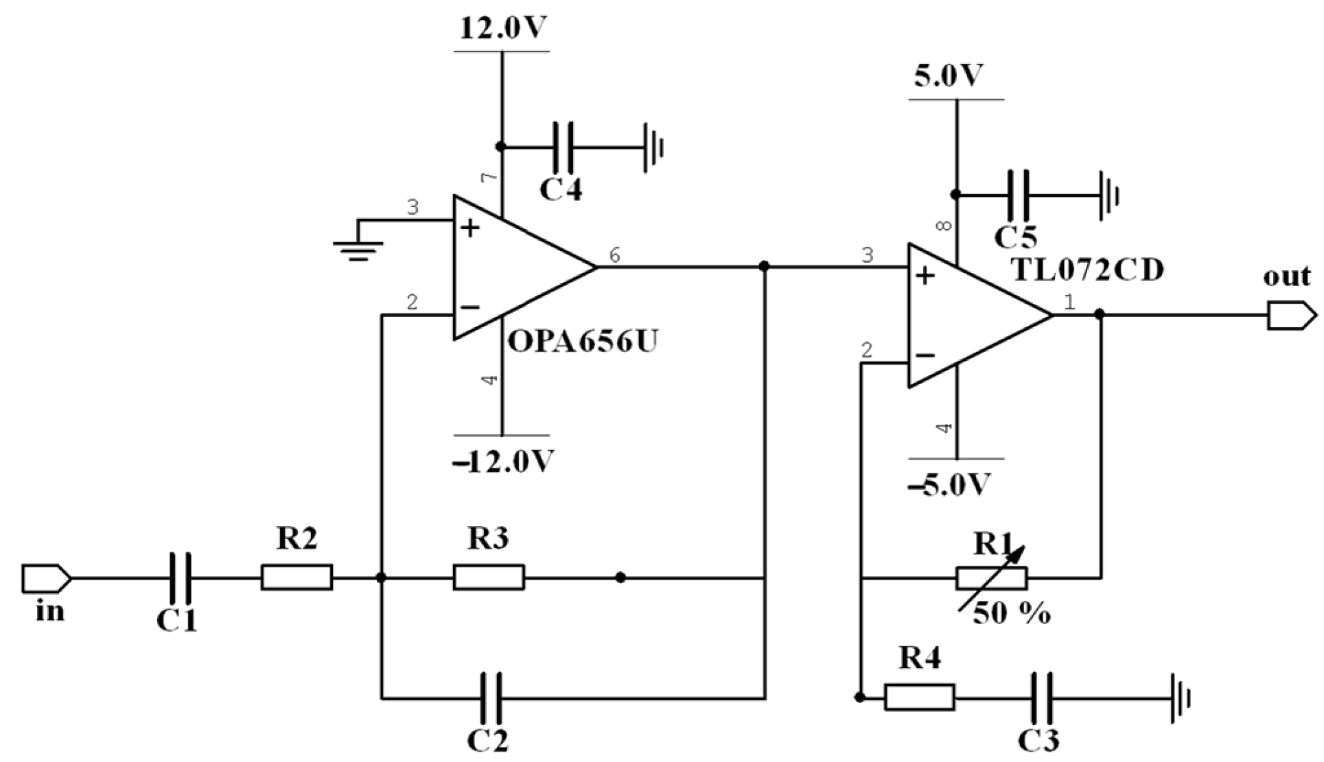
2.3.2. Design of a Material Collision Signal Processing System
- (1)
- Signal amplification module
- (2)
- Core processor module
- (3)
- Analog-to-digital converter
- (4)
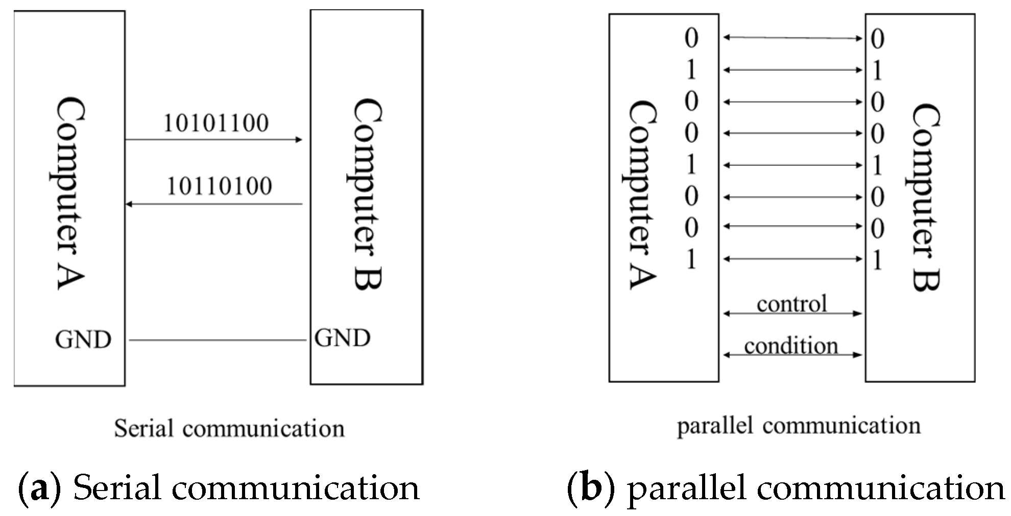
- Communication method
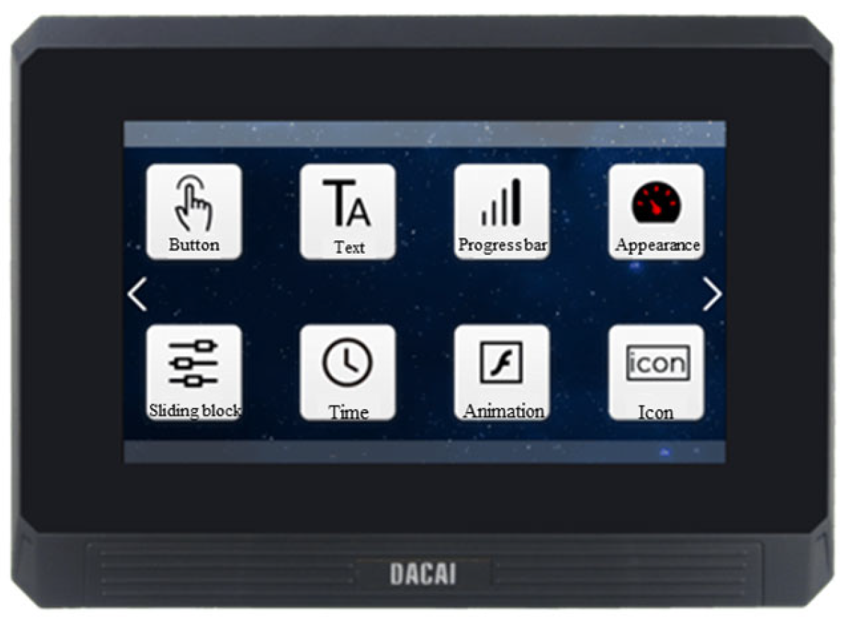
2.3.3. Select the Display Terminal
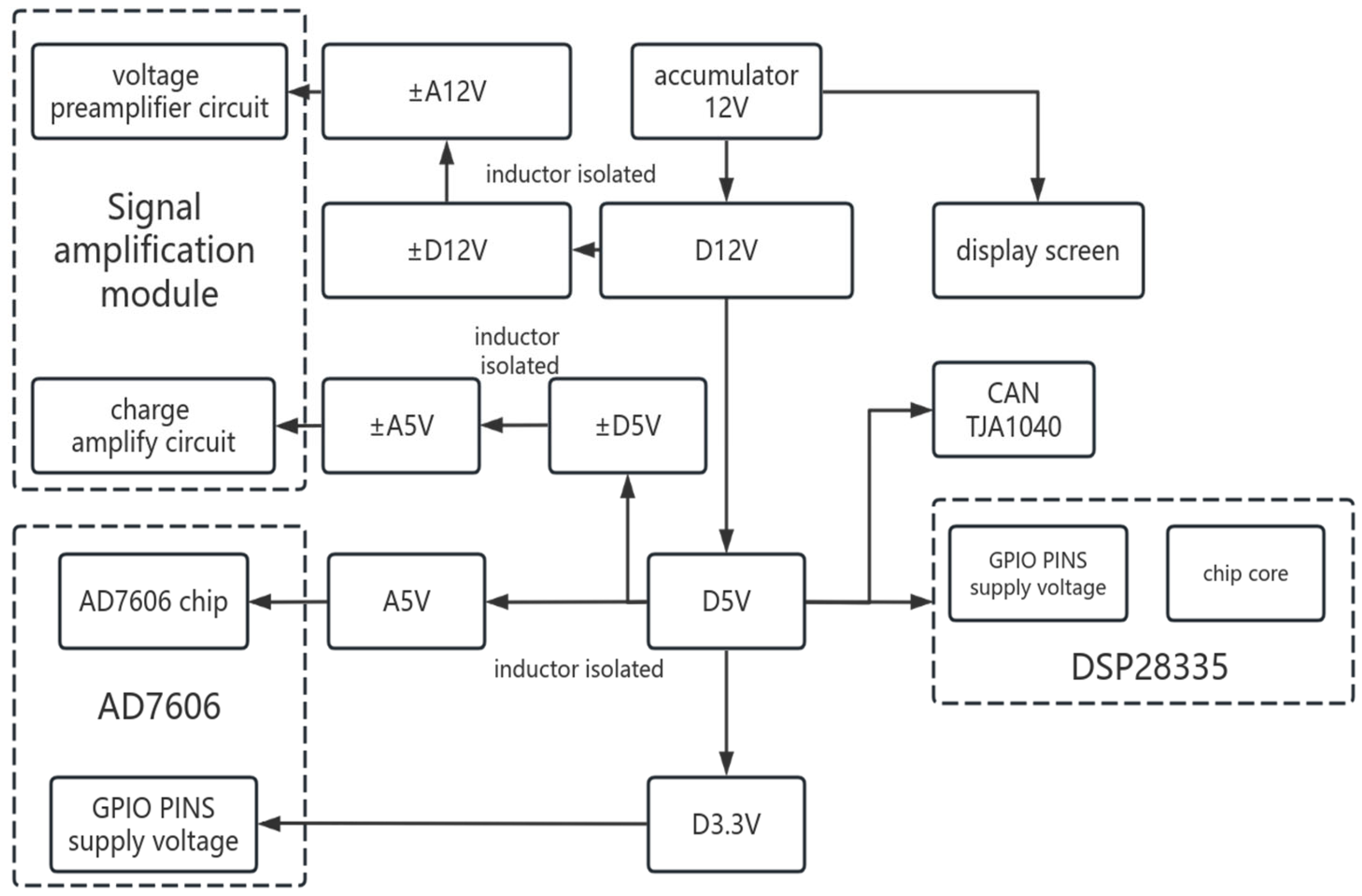
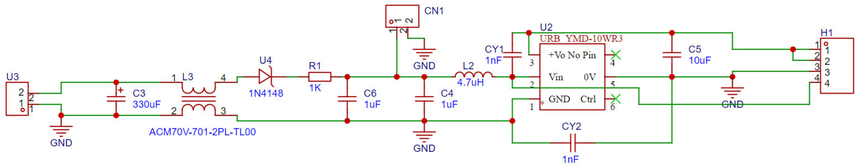
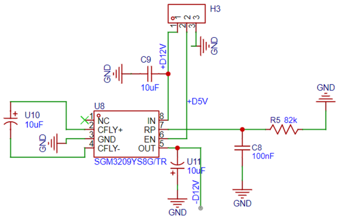
2.3.4. The Design of a Power Supply Circuit
- (1)
- A circuit for converting +12 V input to +5 V output
- (2)
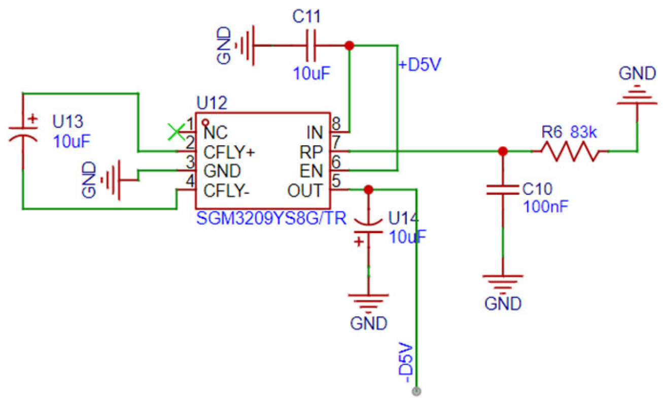
- Negative voltage-generating circuit
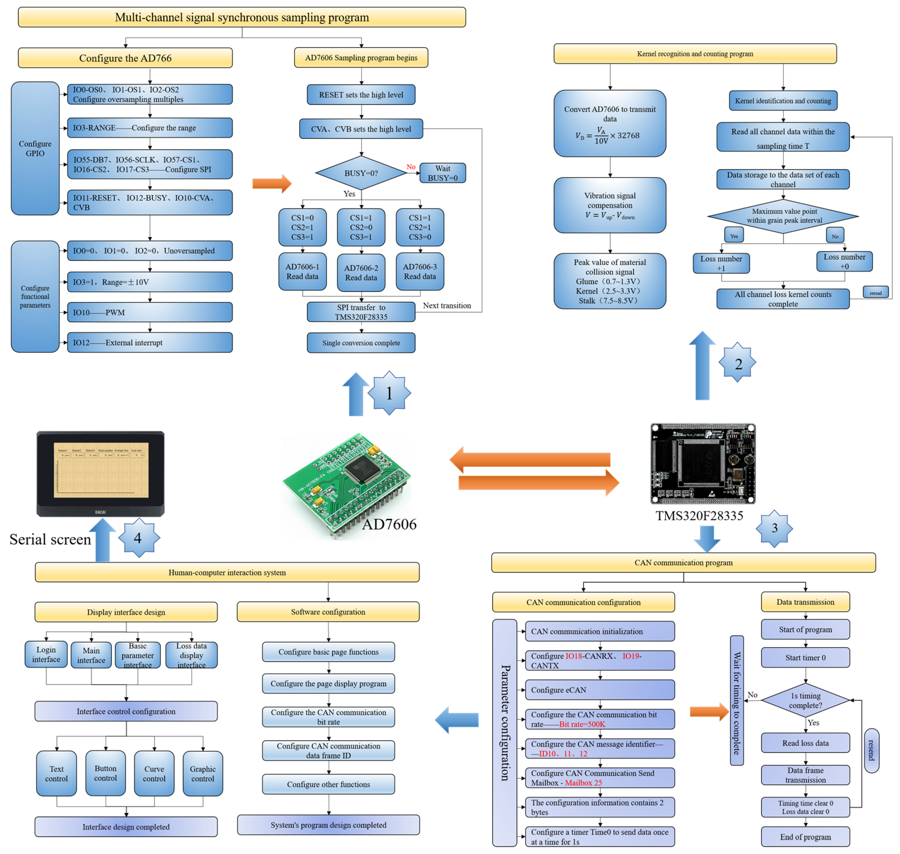
2.4. Software Function Design
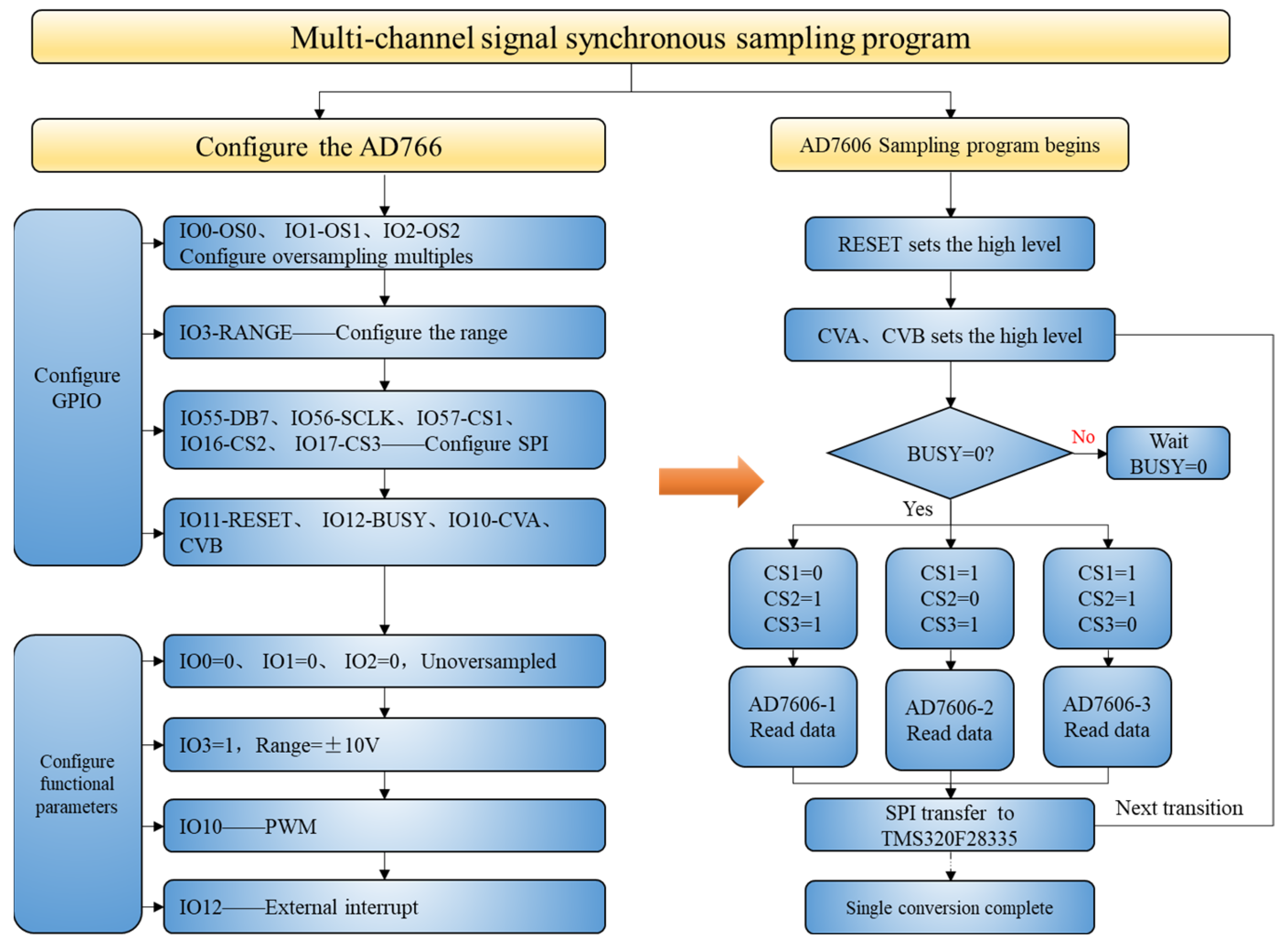
2.4.1. Electrical Signal Data Acquisition Program
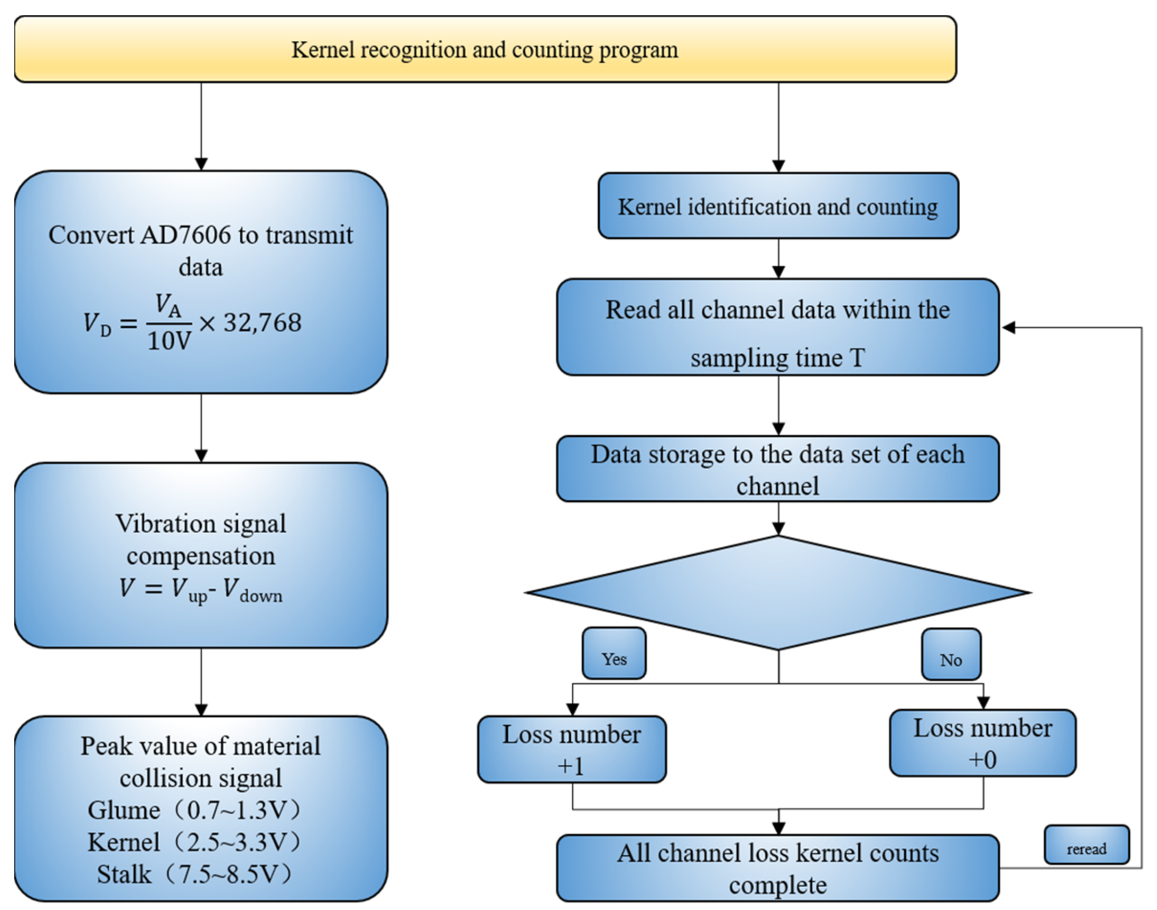
2.4.2. Data Conversion and Signal Compensation Program

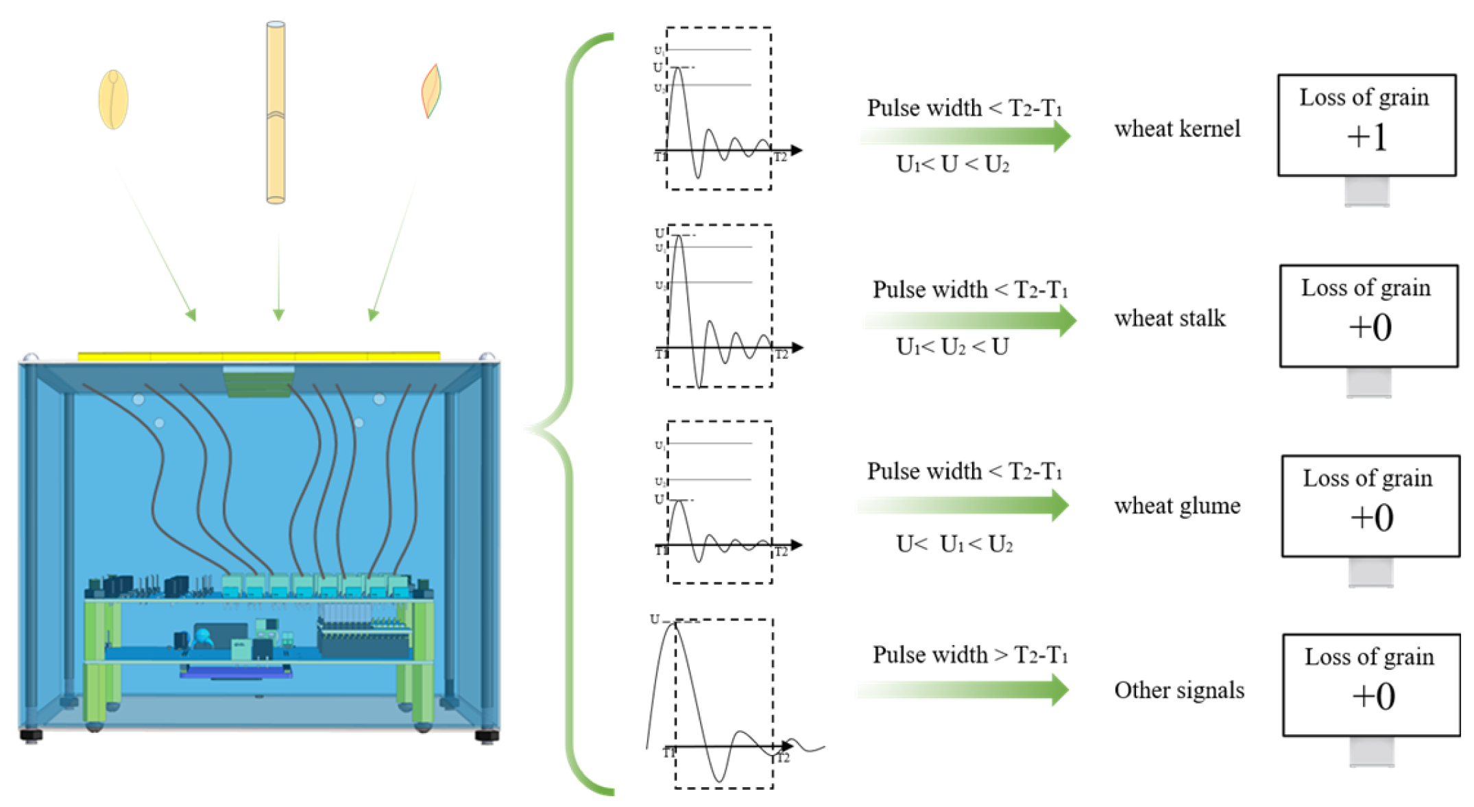
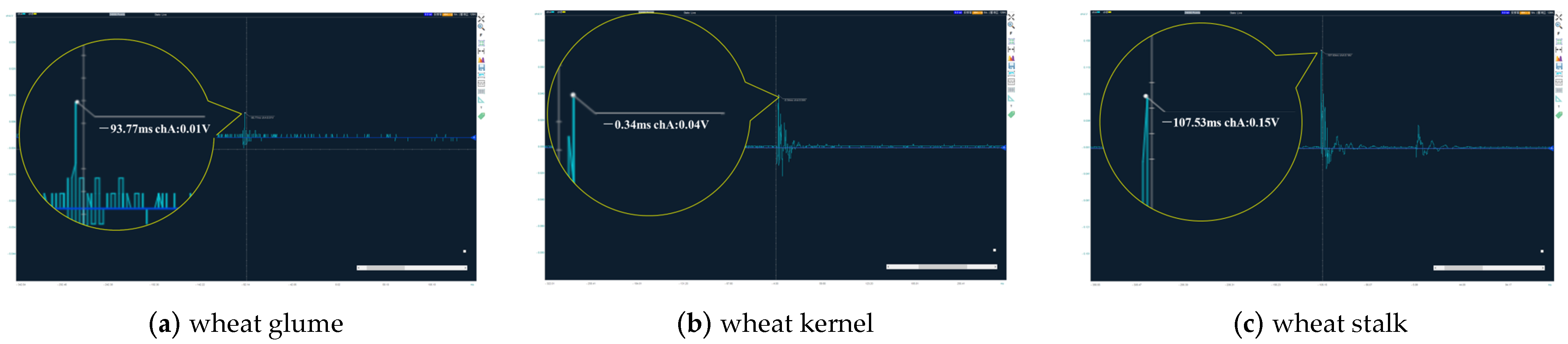
2.4.3. Wheat Grain Identification and Counting Program
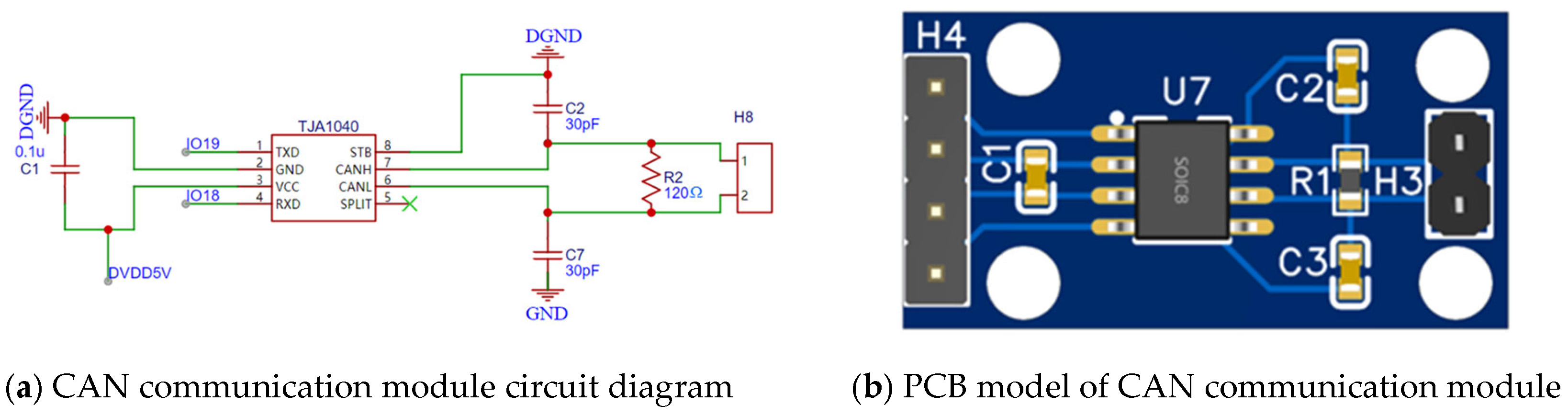
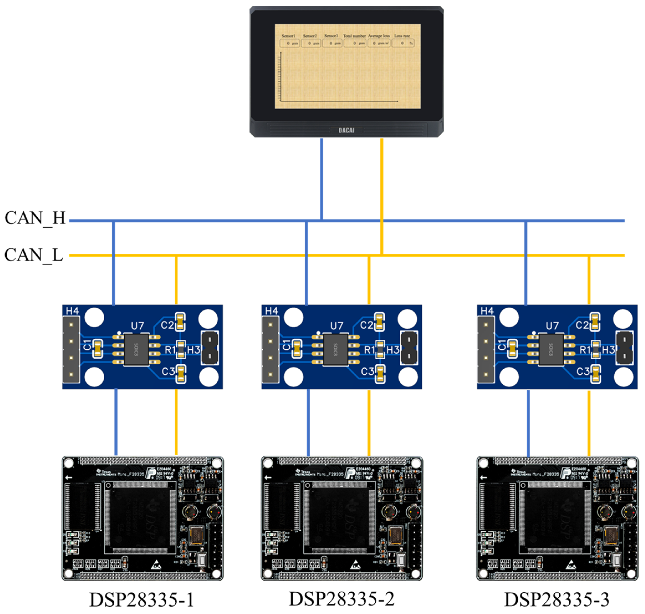
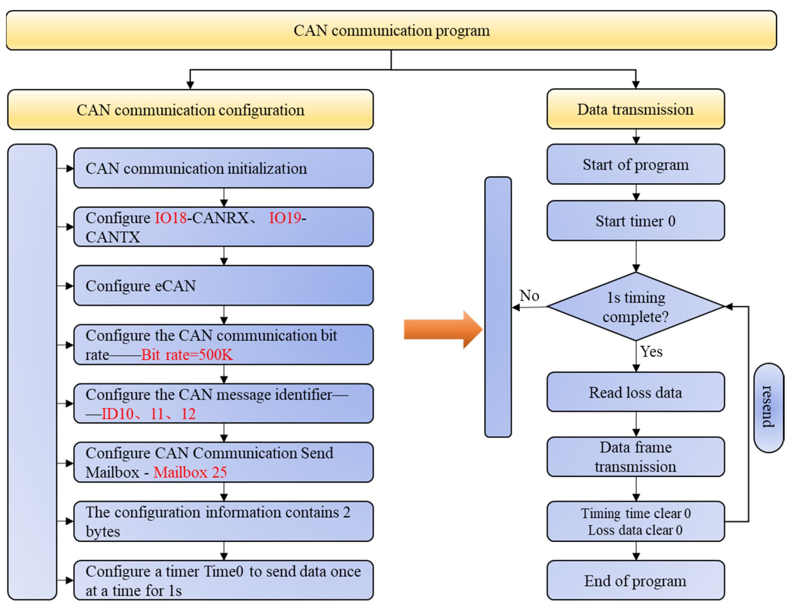
2.4.4. CAN Total Selection Communication Program
2.4.5. Human–Computer Interaction System
3. Results
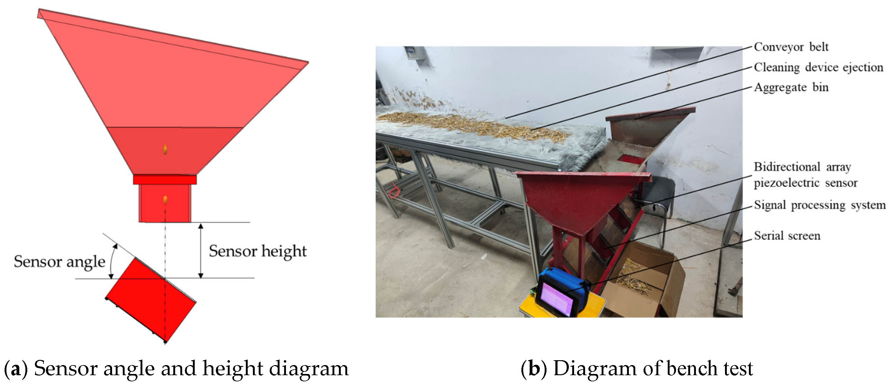
3.1. Bench Test
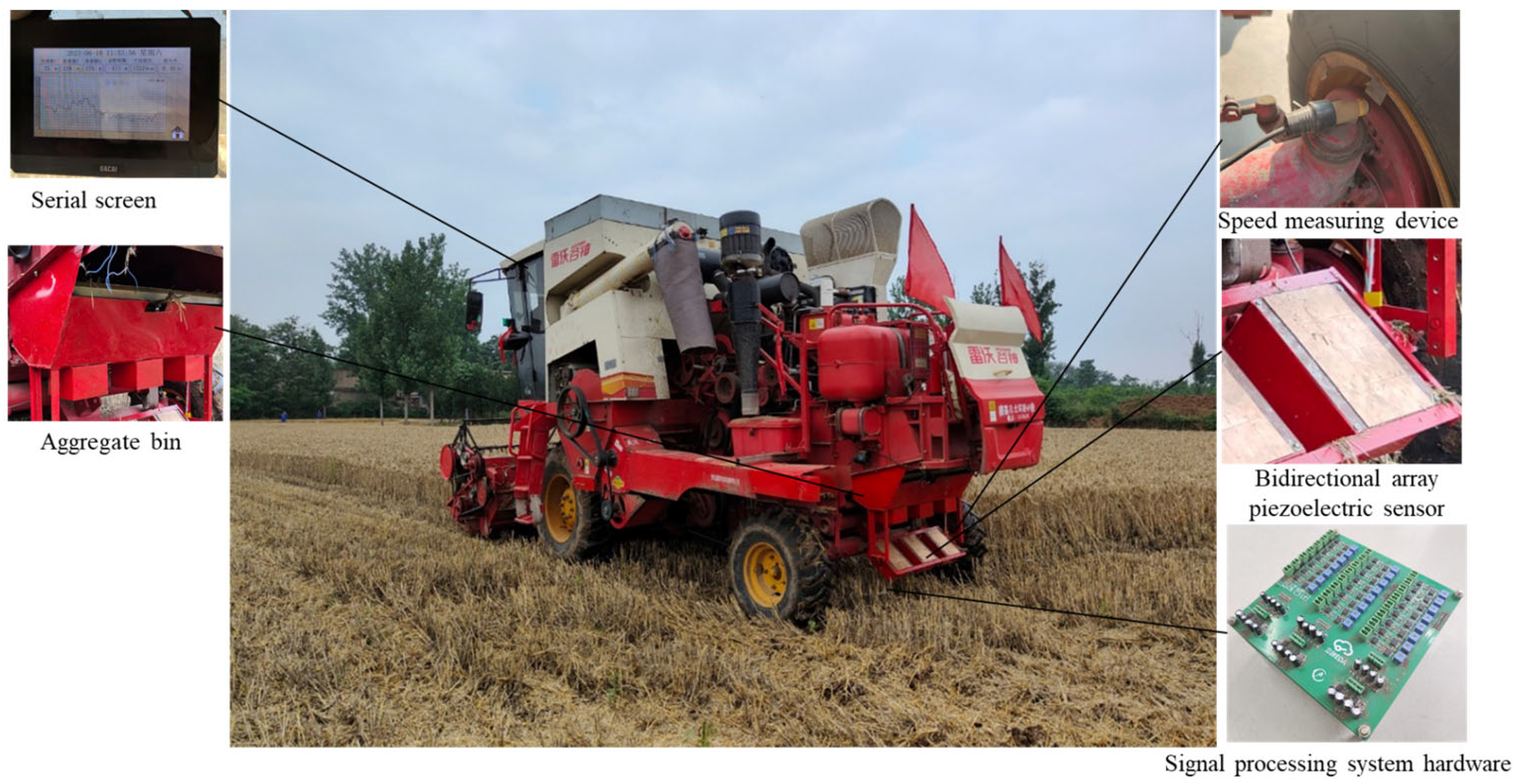
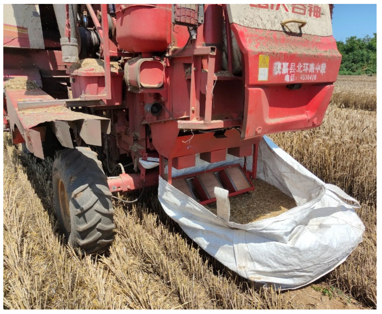
3.2. Field Test
3.3. Test Result
4. Discussion
- (1)
- There were differences between wheat grain parameters used in the R & D period and field harvest.
- (2)
- There was a position difference in the wheat grain impact sensor.
- (3)
- A few wheat varieties and test areas were analyzed.
5. Conclusions
- (1)
- Based on the literature and product data of grain combine loss monitoring devices at home and abroad, this paper expounds and summarizes the grain cleaning loss monitoring technology and method, determines the overall research program and technical route, and carries on the overall design of the wheat combine loss monitoring device. The cleaning loss monitoring device mainly includes a collecting bucket, bidirectional array piezoelectric sensor, vibration signal compensation device, collision signal processing system, human–computer interaction system, etc., which can realize the signal acquisition and identification of the cleaning loss of seeds, display the loss data in real time, remind the driver to adjust the operating parameters of the harvester, and achieve the purpose of collection and loss reduction.
- (2)
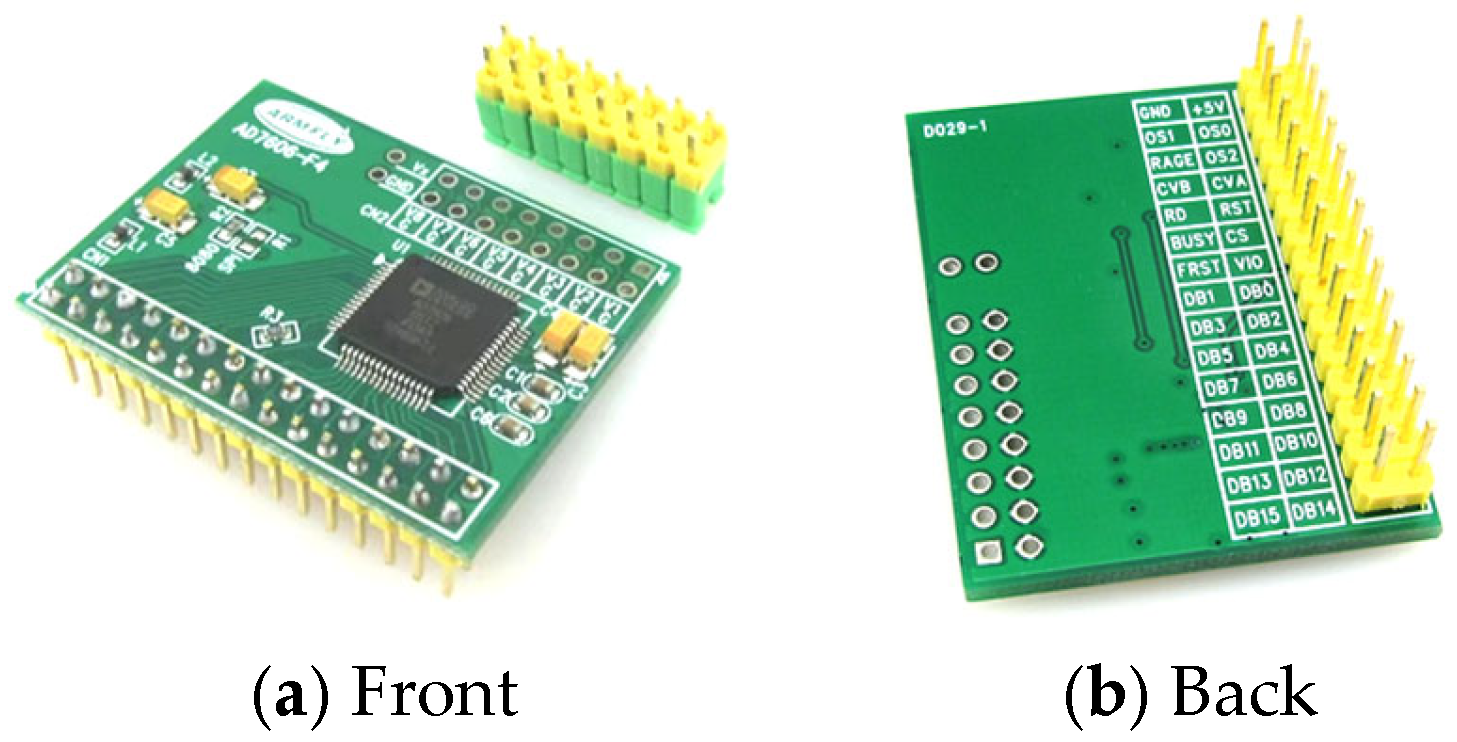
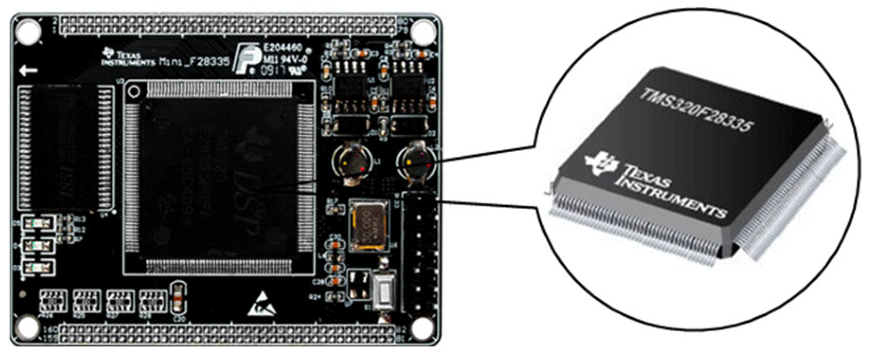
- According to the monitoring requirements of the cleaning loss monitoring device of the wheat combine harvester, the hardware design of the monitoring device was carried out. In order to improve the monitoring capacity of the grain collision sensor and reduce the influence of mechanical vibration on grain recognition accuracy, a bidirectional array piezoelectric sensor and vibration signal compensation device were designed to improve the monitoring capacity of the grain collision sensor. According to the output signal of the sensor, the signal amplifier module is designed, which can realize the signal amplification of 1~100 times. Then, the TMS320F2833 core board is selected as the core processor module, and the collision signals of 20 channels and the vibration signals of 3 channels are collected synchronously through three AD7606 analog-to-digital conversion modules. In order to better transmit the loss data, a CAN communication network is built, and a CAN communication module with a TJA1040 chip as the core is designed to send the cleaning loss data of the combine to the serial screen for data display. According to the power demand of each function module, the power supply circuit is designed to meet the power demand of the cleaning loss monitoring device. The signal amplifier module, AD7606 analog-to-digital conversion module, TMS320F28335 core processor module, and CAN communication module are integrated into the PCB board, and the electrical connection is realized through the PCB board built-in circuit.
- (3)
- The software design is based on the CCS integrated development environment and Visual TFT serial screen development software. The software design realizes the acquisition, identification, counting, and loss data transmission of wheat kernel collision signals; displays the cleaning loss data on the human–computer interactive system; and realizes the real-time monitoring of the cleaning loss of wheat combine. A multi-channel signal synchronous acquisition program was designed to collect signals from 23 output channels of a bidirectional array piezoelectric sensor and vibration signal compensation device at a sampling rate of 40 kHz, and SPI communication transmitted the collected data to the TMS320F28335 core processor for vibration signal compensation program processing. The kernel identification and counting program with the kernel collision signal peak value of 2.5 V~3.3 V as the index is completed. Finally, the data frames with ID values of 10, 11, and 12 are transmitted to the human–computer interaction system by CAN bus at a communication rate of 500 Kbps for loss data display. When the cleaning loss exceeds the regulation, the driver is reminded to adjust the operating parameters of the harvester to reduce the cleaning loss.
- (4)
- In order to verify the accuracy, reliability, and stability of the cleaning loss monitoring device, bench tests and field tests were carried out. The bench test shows that the identification error rate of a bidirectional array piezoelectric sensor is 5.19% when the inclination angle is 44° and the center point is 300 mm away from the material outlet. In the field test, the overall operation of the device was stable without any fault. The error rate of kernel identification was less than 8%, and the average error rate was 6.69%, which met the design requirements of the harvester cleaning loss monitoring device and could remind the driver to adjust the operating parameters of the harvester to achieve the purpose of loss reduction.
Author Contributions
Funding
Institutional Review Board Statement
Data Availability Statement
Acknowledgments
Conflicts of Interest
References
- Sun, Y.; Hu, S.; Li, Z.; Shim, J.; Lee, J. Study on the influencing factors of wheat import trade in China. J. Korea Acad. -Ind. Coop. Soc. 2022, 2, 608–620. [Google Scholar]
- JB/T 5117-2017; Technical Conditions of Full-Feeding Combine Harvester. China Machine Press: Beijing, China, 2017.
- Jin, C.Q.; Li, Q.L.; Ni, Y.L.; Wang, T.E.; Yin, X. Experimental study on double air outlet multi-ducts cleaning device of wheat combine harvester. Trans. Chin. Soc. Agric. Eng. 2020, 36, 26–34. [Google Scholar]
- Li, Y.; Xue, Z.; Xu, L.Z.; Li, Y.M.; Qiu, X.; Wang, Y.F. Research progress on the monitoring methods of the separating loss in grain combine harvester. J. Intell. Agric. Mech. 2020, 1, 13–23. [Google Scholar]
- Xu, J.J. Research on the Experimental Method of Combine Harvester Entrainment Loss Monitoring; Jiangsu University: Zhenjiang, China, 2010. [Google Scholar]
- Jie, Z. Prospect of Test Method of Grain Random Loss Rate in China. J. Agric. Mech. Res. 2009, 31, 5–9. [Google Scholar]
- Jie, Z.; Liu, H.J.; Hou, F.Y. Research advances and prospects of combine on precision agriculture in China. Trans. Chin. Soc. Agric. Eng. 2005, 21, 179–182. [Google Scholar]
- Botterill John, R.; Kepkay Leslie, L.; Dodd Philip, L.; Radbumn William, J. Combine Grain Loss Signal. Massey Ferguson Services. U.S. Patent 3,593,720, 20 July 1971. [Google Scholar]
- Northup, M.; Moore, D.L.; Shaver, J.L. Grain Loss Monitor. U.S. Patent 3,935,866, 25 October 1976. [Google Scholar]
- Liu, C.; Leonard, J. Monitoring actual grain loss from an axial flow combine in real time. Comput. Electron. Agric. 1993, 9, 231–242. [Google Scholar] [CrossRef]
- Batcheller, B.D.; Gelinske, J.; Nystuen, P.A.; Reich, A.A. System and Method for Determining Material Yield and/or Loss from a Harvesting Machine Using Acoustic Sensors. U.S. Patent 9,474,208, 7 January 2016. [Google Scholar]
- Mao, H.P.; Ni, J. Finite Element Analysis and Measurement for Array Piezocrystals Grain Losses Sensor. Trans. Chin. Soc. Agric. Mach. 2008, 39, 123–126. [Google Scholar]
- Zhang, T. The Study of Information Processing Platform of Combine Based on Arm9-Linux Embedded System. Master’s Thesis, Jiangsu University, Zhenjiang, China, 2009. [Google Scholar]
- Zhao, Z.; Li, Y.M.; Chen, J.; Xu, J.J. Grain separation loss monitoring system in combine harvester. Comput. Electron. Agric. 2011, 76, 183–188. [Google Scholar] [CrossRef]
- Zhou, L.M.; Zhang, X.C.; Liu, C.Y.; Yuan, Y.W. Design of PVDF Sensor Array for Grain Loss Measuring. Trans. Chin. Soc. Agric. Mach. 2010, 41, 167–171. [Google Scholar]
- Li, Y.M.; Liang, Z.W.; Zhao, Z.; Chen, Y. Real-time Monitoring System of Grain Loss in Combine Harvester. Trans. Chin. Soc. Agric. Mach. 2011, 42, 99–102. [Google Scholar]
- Sun, Y. The Basie Characteristics of Grain Impact Sensor Utilizing Two Crossed PVDF Films; Zhejiang University: Hangzhou, China, 2018. [Google Scholar]
- Gao, L.W.; Xu, S.W.; Li, Z.M.; Cheng, S.K.; Yu, W.; Zhang, Y.E.; Li, D.H.; Wang, Y.; Wu, C. Study on the characteristics and potential of postpartum loss of major grain crops in China. Acta Agric. Eng. 2016, 32, 1–11. [Google Scholar]
- Wei, H.T. Wheat mechanized harvesting technology and harvesting loss reduction measures. Seed Sci. Technol. 2024, 42, 128–130+151. [Google Scholar]
- Xu, L.Z.; Li, Y.; Li, Y.M.; Chai, X.Y.; Qiu, J. Research Progress on Cleaning Technology and Device of Grain Combine Harvester. Trans. Chin. Soc. Agric. Mach. 2019, 50, 1–16. [Google Scholar]
- Zhang, T.; Zhao, D.A.; Zhou, T. Application of lmage Processing on Combine Harvester Attachment Loss. J. Agric. Mech. Res. 2009, 31, 70–72. [Google Scholar]
- Zhang, X.F. Research and development suggestions on the development history of piezoelectric sensors. Transducer Microsyst. Technol. 1984, 63–67. [Google Scholar]
- Ni, J.; Mao, H.P.; Li, P.P. Design of Intelligent Grain Cleaning Losses Monitor Based on Array Piezocrystals. Trans. Chin. Soc. Agric. Mach. 2010, 41, 175–177. [Google Scholar]
- Zhang, J.; Li, X.D.; Ren, Y.F. Study on Preparation and Electrical Properties of PMN-PZT Piezoelectric Ceramics. J. Hubei Polytech. Univ. 2022, 38, 28–34. [Google Scholar]
- Li, Y.M.; Chen, Y.; Zhao, Z.; Xu, L.Z. Monitoring Method and Device for Cleaning Loss of Combine Harvester. Trans. Chin. Soc. Agric. Mach. 2013, 44, 7–11. [Google Scholar]
- Zhao, Z.; Li, Y.M.; Liang, Z.W.; Chen, Y. Optimum design of grain impact sensor utilising polyvinylidene fluoride films and a floating raft damping structure. Biosyst. Eng. 2012, 112, 227–235. [Google Scholar] [CrossRef]
- Liang, Z.W.; Li, Y.M.; Xu, L.Z.; Zhao, Z. Sensor for monitoring rice grain sieve losses in combine harvesters. Biosyst. Eng. 2016, 147, 51–66. [Google Scholar] [CrossRef]
- Liang, Z.W.; Li, Y.M.; Zhao, Z.; Xu, L.Z. Structure Optimization of a Grain Impact Piezoelectric Sensor and Its Application for Monitoring Separation Losses on Tangential-Axial Combine Harvesters. Sensors 2015, 15, 1496–1517. [Google Scholar] [CrossRef]
- Li, J.F. Improvement design of the structure of combine harvester grain loss sensor and laboratory calibration. Agric. Equip. AMP Veh. Eng. 2006, 11, 10–13. [Google Scholar]
- Zhou, J.; Cong, B.H.; Liu, C.L. Elimination of vibration noise from an impact-type grain mass flow sensor. Precis. Agric. 2014, 15, 627–638. [Google Scholar] [CrossRef]
- Hansen, S.K.E. Design and Experimental Investigation of Charge Amplifiers for Ultrasonic Transducers. The Arctic University of Norway, 2014. Available online: https://hdl.handle.net/10037/6783 (accessed on 11 April 2024).
- Meng, Y. Design and Implementation of a Multi-Channel Measurement System Based on FPGA and eMMC. Master’s Thesis, North University of China, Taiyuan, China, 2024. [Google Scholar]
- Leens, F. An introduction to I2C and SPI protocols. IEEE Instrum. Meas. Mag. 2009, 12, 8–13. [Google Scholar] [CrossRef]
- Seo, S. Performance Analysis of CAN-FD Based Network Against Network Topology. IEMEK J. Embed. Syst. Appl. 2017, 12, 351–359. [Google Scholar] [CrossRef]
- Cao, R. Research on Signal Processing System of Multichannel PVDF Piezoelectric Thin Film Grain Loss Sensor Based on DSP. Master’s Thesis, Zhejiang University, Hangzhou, China, 2020. [Google Scholar] [CrossRef]
- Xu, L.Z.; Wei, C.C.; Liang, Z.W.; Chai, X.Y.; Li, Y.M.; Liu, Q. Development of rapeseed cleaning loss monitoring system and experiments in a combine harvester. Biosyst. Eng. 2019, 178, 118–130. [Google Scholar] [CrossRef]
- Wei, D.X.; Wu, C.Y.; Jiang, L.; Wang, G.; Chen, H. Design and Test of Sensor for Monitoring Corn Cleaning Loss. Agriculture 2023, 13, 663. [Google Scholar] [CrossRef]
- Tang, Z.; Li, Y.M.; Zhao, Z.; Liang, Z.W.; Chen, Y. Effect of different installation positions of entrainment loss sensor on grain detection accuracy. Trans. Chin. Soc. Agric. Eng. 2012, 28, 46–52. [Google Scholar]


| Performance Index | Parameter |
|---|---|
| Relative dielectric constant | 3400 |
| Planar electromechanical coupling factor | 0.62 |
| Young’s modulus | 56 × 109 N/m2 |
| Poisson ratio | 0.36 |
| Density | 7.6 × 10³ kg/m3 |
| PAR/SER/BYTE SEL Pins | DB15 Pins | Interface Mode |
|---|---|---|
| 0 | 0 | Parallel interface |
| 1 | 0 | Serial interface |
| 1 | 1 | Parallel byte interface |
| AD766 Pins | TMS320F28335 Pins | Function |
|---|---|---|
| OS1, OS2, and OS3 | GPIO0, GPIO1, and GPIO2 | Set the oversampling rate |
| RANGE | GPIO3 | Set the sampling voltage range |
| CVA and CVB | GPIO10 | Control begins to convert |
| RST | GPIO11 | Reset |
| RD | GPIO56 | Serial clock input |
| BUSY | GPIO12 | Busy conversion |
| CS (CS1, CS2, and CS3) | GPIO57, GPIO16, and GPIO17 | Chip selection signal line |
| DB7 | GPIO55 | Data output pin |
| DB15 | GND | Communication mode selection pins |
| RS-232 | RS-485 | CAN | |
|---|---|---|---|
| Communication distance | 30 m (max) | 3 km (max) | 10 km (max) |
| transmission rate | 20 Kbps | 10 Mbps (max) | 1 Mbps (max) |
| Network structure | Single-master | Single-master | Multi-master |
| Node failure | Influence the whole | Influence the whole | Does not influence the whole |
| Item | The Parameter of Product |
|---|---|
| Power supply | 9~36 V DC voltage |
| Communication interface | RS-485, CAN, and Ethernet |
| Development mode | LUA secondary development |
| Audio format | MP3 |
| Memory space | 1 GB of storage space |
| Electrical Devices | Power Supply Demand |
|---|---|
| OPA656 chip | ±5 V |
| TL072 chip | ±12 V |
| DSP28335 core processor module | +5 V |
| AD7606 module | +5 V |
| TJA1040 chip | +5 V |
| Serial display screen | +9 V~+36 V |
| Code | Experimental Factors | ||
|---|---|---|---|
| Grain Numbers (Grain) | Sensor Angle (°) | Sensor Height (mm) | |
| −1 | 100 | 30 | 100 |
| 0 | 200 | 45 | 200 |
| 1 | 300 | 60 | 300 |
| No. | Experimental Factors | Error Rate (%) | ||
|---|---|---|---|---|
| Grain Numbers (Grain) | Sensor Angle (°) | Sensor Height (mm) | ||
| 1 | −1 | 0 | 1 | 5.4 |
| 2 | −1 | 0 | −1 | 6 |
| 3 | −1 | 1 | 0 | 6.3 |
| 4 | −1 | −1 | 0 | 5.7 |
| 5 | 0 | −1 | −1 | 6.9 |
| 6 | 0 | 1 | −1 | 7.7 |
| 7 | 0 | 0 | 0 | 6.2 |
| 8 | 0 | −1 | 1 | 6.4 |
| 9 | 0 | 0 | 0 | 6.1 |
| 10 | 0 | 1 | 1 | 6.6 |
| 11 | 0 | 0 | 0 | 6.1 |
| 12 | 0 | 0 | 0 | 6.7 |
| 13 | 0 | 0 | 0 | 6.1 |
| 14 | 1 | 0 | 1 | 7.1 |
| 15 | 1 | 0 | −1 | 7.4 |
| 16 | 1 | −1 | 0 | 7.5 |
| 17 | 1 | 1 | 0 | 8.6 |
| Source | Sum of Square | df | Mean Square | F-Value | p-Value |
|---|---|---|---|---|---|
| Model | 10.12 | 9 | 1.12 | 15.15 | 0.0008 |
| A | 6.48 | 1 | 6.48 | 87.31 | <0.0001 |
| B | 0.91 | 1 | 0.91 | 12.28 | 0.0099 |
| C | 0.78 | 1 | 0.78 | 10.53 | 0.0142 |
| AB | 0.063 | 1 | 0.063 | 0.84 | 0.3893 |
| AC | 0.022 | 1 | 0.022 | 0.30 | 0.5990 |
| BC | 0.090 | 1 | 0.090 | 1.21 | 0.3072 |
| A2 | 0.14 | 1 | 0.14 | 1.84 | 0.2173 |
| B2 | 1.54 | 1 | 1.54 | 20.77 | 0.0026 |
| C2 | 0.013 | 1 | 0.013 | 0.17 | 0.6911 |
| Residual | 0.52 | 7 | 0.074 | ||
| Lack of fit | 0.25 | 3 | 0.083 | 1.21 | 0.4129 |
| Errors | 0.27 | 4 | 0.068 |
| No. | Model Predicted Value (%) | Test Value (%) | Relative Error (%) |
|---|---|---|---|
| 1 | 5.19% | 5.25% | 1.16% |
| 2 | 5.14% | 0.96% | |
| 3 | 5.18% | 0.19% |
| Number | Monitoring Losses (Grains) | Measurement Loss (Grains) | Omission Factor K |
|---|---|---|---|
| 1 | 5150 | 6205 | 0.83 |
| 2 | 5534 | 6218 | 0.89 |
| 3 | 5334 | 6132 | 0.87 |
| 4 | 5412 | 6081 | 0.89 |
| 5 | 5081 | 5978 | 0.85 |
| No. | Monitoring Losses (Grains) | Monitoring Loss Rate (%) | Measurement Loss (Grains) | Measurement Loss Rate (%) | Monitoring Error (%) |
|---|---|---|---|---|---|
| 1 | 5865 | 0.98% | 6252 | 1.04% | 6.19% |
| 2 | 6383 | 1.07% | 5914 | 0.99% | 7.93% |
| 3 | 5763 | 0.96% | 6128 | 1.03% | 5.96% |
Disclaimer/Publisher’s Note: The statements, opinions and data contained in all publications are solely those of the individual author(s) and contributor(s) and not of MDPI and/or the editor(s). MDPI and/or the editor(s) disclaim responsibility for any injury to people or property resulting from any ideas, methods, instructions or products referred to in the content. |
© 2024 by the authors. Licensee MDPI, Basel, Switzerland. This article is an open access article distributed under the terms and conditions of the Creative Commons Attribution (CC BY) license (https://creativecommons.org/licenses/by/4.0/).
Share and Cite
Qu, Z.; Lu, Q.; Shao, H.; Le, J.; Wang, X.; Zhao, H.; Wang, W. Design and Test of a Grain Cleaning Loss Monitoring Device for Wheat Combine Harvester. Agriculture 2024, 14, 671. https://doi.org/10.3390/agriculture14050671
Qu Z, Lu Q, Shao H, Le J, Wang X, Zhao H, Wang W. Design and Test of a Grain Cleaning Loss Monitoring Device for Wheat Combine Harvester. Agriculture. 2024; 14(5):671. https://doi.org/10.3390/agriculture14050671
Chicago/Turabian StyleQu, Zhe, Qi Lu, Haihao Shao, Jintao Le, Xilong Wang, Huihui Zhao, and Wanzhang Wang. 2024. "Design and Test of a Grain Cleaning Loss Monitoring Device for Wheat Combine Harvester" Agriculture 14, no. 5: 671. https://doi.org/10.3390/agriculture14050671
APA StyleQu, Z., Lu, Q., Shao, H., Le, J., Wang, X., Zhao, H., & Wang, W. (2024). Design and Test of a Grain Cleaning Loss Monitoring Device for Wheat Combine Harvester. Agriculture, 14(5), 671. https://doi.org/10.3390/agriculture14050671