Inorganic Materials by Atomic Layer Deposition for Perovskite Solar Cells

Advanced Materials Division, Korea Research Institute of Chemical Technology (KRICT), Daejeon 34114, Korea
Nanomaterials 2021, 11(1), 88; https://doi.org/10.3390/nano11010088
Submission received: 1 December 2020
/
Revised: 26 December 2020
/
Accepted: 28 December 2020
/
Published: 3 January 2021
(This article belongs to the Special Issue Perovskite Nanostructures: From Material Design to Applications)
Abstract
:Organic–inorganic hybrid perovskite solar cells (PSCs) have received much attention with their rapid progress during the past decade, coming close to the point of commercialization. Various approaches in the process of PSC development have been explored with the motivation to enhance the solar cell power conversion efficiency—while maintaining good device stability from light, temperature, and moisture—and simultaneously optimizing for scalability. Atomic layer deposition (ALD) is a powerful tool in depositing pinhole-free conformal thin-films with excellent reproducibility and accurate and simple control of thickness and material properties over a large area at low temperatures, making it a highly desirable tool to fabricate components of highly efficient, stable, and scalable PSCs. This review article summarizes ALD’s recent contributions to PSC development through charge transport layers, passivation layers, and buffer and recombination layers for tandem applications and encapsulation techniques. The future research directions of ALD in PSC progress and the remaining challenges will also be discussed.
1. Introduction
As solar energy is the most abundant energy resource available to humankind, various photovoltaic (PV) technologies have been investigated by researchers over the past years with the common motivation to efficiently and cost-effectively convert solar energy into electricity. Organic–inorganic hybrid perovskite solar cells (PSCs) make up an exciting field of PV technology research due to its speedy progress during the past decade arriving close to the point of commercialization. Although PSCs have shown promising results in terms of theirs rapid progress in power conversion efficiency, already at 25.5% for unit cells [1], they are different from other PV technologies as they display other challenges especially towards long-term stability of the working devices from both external and internal factors. Device deterioration from internal factors include ion migration from the perovskite layer and from dopants of hole transport layers diffusing out into the perovskite, whereas external factors include deterioration from exposure to light, elevated temperatures, and air (moisture and oxygen) [2,3,4,5,6,7,8,9,10]. In order for the actual commercialization of PSCs to occur, optimization of the following aspects will be required: high efficiency, long-term stability, possible large-area coating techniques, consideration of semitransparent and tandem applications, and nontoxicity and low-cost of the materials and fabrication processes.
Atomic layer deposition (ALD) is a powerful tool for growing reproducible conformal pinhole-free high-quality thin-films of inorganic materials. ALD has the advantage of precise fine control of the film thickness and materials properties, such as stoichiometry, morphology, and doping [11,12,13,14,15]. While chemical vapor deposition (CVD) and physical vapor deposition (PVD), including thermal evaporation, e-beam evaporation, molecular beam epitaxy, pulsed laser deposition, and sputtering, have been popular deposition methods in industry, ALD has gained much attention with ultra-thin or pinhole-free conformal coating becoming more important. Film formation by PVD methods are usually by direct transport of the source to the substrate through the gas phase, while film formation by CVD involves chemical reaction between mixed gas sources on a substrate. In comparison to PVD and CVD, ALD is a low-vacuum and low-temperature deposition technique, which allows excellent conformal and uniform coating of 3D structures and precise control of film thickness due to its self-limiting chemisorption of precursors during the ALD cycle. However, such high precision leads to high usage of the ALD precursors and co-reactants, which lead to waste of materials, as approximately 60% of the precursor pulse is wasted in the ALD growth process. Another disadvantage is the cost-effectiveness of ALD in commercial use due to its low deposition rates. Such challenges have been partially overcome by spatial-ALD [16,17].
Due to its possibilities for deposition over large areas at low temperatures, ALD has already shown to be useful in various other applications, such as microelectronics, batteries, and other leading PV technologies, including crystalline silicon and copper indium gallium diselenide (CIGS) thin-film solar cells [18,19,20,21,22]. Thus, ALD is a highly attractive tool to fabricate components of layers in PSCs, and its contribution to the advancement of PSC should be fully utilized and explored. This review article will summarize and highlight cases where ALD has been applied to the development of PSCs and provide insight into the current challenges and future of ALD in the development of PSCs.
As the perovskite and organic transport layers are particularly susceptible to elevated temperatures and exposure to certain ALD precursors under low vacuum, this review will be divided into parts focusing on the developments below and above the perovskite layer. As summarized in the schematic graphic in Figure 1, ALD can be applied in PSCs for the electrodes, charge transport layers (CTLs) below and above the perovskite, passivation layer, buffer layer, and encapsulation. The corresponding section numbers in this review for the application of ALD for each layer are shown in the schematic. First, in Section 2, we investigate the cases where ALD processes were adopted for the deposition of layers under the perovskite layer as electron transport layers (ETLs, Section 2.1.1) and hole transport layers (HTLs, Section 2.1.2).
In Section 3, we explore the developments made for ALD utilized for layers above the perovskite absorber as CTLs (Section 3.1), passivation or barrier layers (Section 3.2), recombination layers or bottom electrodes (Section 3.3), buffer layers in semitransparent and tandem applications (Section 3.4), and encapsulation (Section 3.5). The efforts of ALD in halide perovskite light emitting diodes will also be discussed (Section 4). Variations of ALD techniques, such as pulsed-chemical vapor deposition (pulsed-CVD) and spatial ALD (s-ALD), will be further discussed in Section 5, and conclusions and future outlooks will be discussed in Section 6.
2. ALD below the Perovskite Layer
2.1. Charge Transport Layers below the Perovskite Layer
Despite the many advantages of ALD, there are certain issues that get introduced when dealing with PSCs as organic charge transport layers and the perovskite absorber are susceptible to damage from exposure to elevated temperatures and certain ALD precursors in the presence of low vacuum levels of approximately hundreds of millitorrs. However, this is not as much of a problem when applying ALD to grow films below the perovskite layer. Various studies in the literature of ALD films incorporated into PSCs for layers below the perovskite absorber are summarized in Table 1. We will first begin with discussing charge transport layers (including ETLs and HTLs) below the perovskite layer and then move onto layers above the perovskite absorber in Section 3.
2.1.1. Electron Transport Layers
The most commonly used materials for ETLs in n-i-p structured PSCs, include mesoporous titanium dioxide (TiO2) for mesoscopic structures, and tin dioxide (SnO2) by chemical bath deposition (CBD) or spin-coating nanoparticles for planar structures [23]. Various laboratories have explored alternatively growing ETLs by ALD using materials such as TiO2, SnO2, zinc oxide (ZnO), and niobium oxide (Nb2O5). Perovskite solar cells with ALD SnO2 using deposition temperatures in the range of 100–120 °C have been demonstrated by tetrakis-dimethyl-amine tin (TDMASn) and ozone (O3) or oxygen (O2) plasma, as the tin and oxygen precursors, respectively, reaching power conversion efficiencies (PCE, η) over 20% [24]. ALD SnO2 without any post-treatments or additional electron transporting materials result in a PCE of 20% when using a triple cation perovskite followed by 2,2′,7,7′-tetrakis-(N,N-di-4-methoxyphenylamino)-9,9′-spirobifluorene (spiro-OMeTAD) and gold (Au), as shown in Figure 2a–c. ALD SnO2 followed by fullerene-self-assembly monolayer (C60-SAM) is reported to effectively improve the charge collection at the ETL/perovskite interface, the current density vs. voltage (J–V) scan hysteresis is still an issue [25]. Post-annealing ALD SnO2 at 100 °C in air resulted in improved electron mobility of SnO2, and consequently enhanced the PCE and reduced the J–V hysteresis (Figure 2d), resulting in PCE over 20% (Figure 2e).
Some reports have also demonstrated ALD n-type materials to be effective in surface treatment of the transporting conducting oxide (TCO)/ETL or ETL/perovskite interfaces, instead of completely replacing the conventional nanoparticle SnO2 (np-SnO2) or bilayer TiO2 structures, which consists of a compact TiO2 layer (c-TiO2) followed by a mesoporous TiO2 (mp-TiO2) layer. Previous studies investigated ALD TiO2 mostly in between the TCO, usually indium tin oxide (ITO) or fluorine-doped tin oxide (FTO), and mp-TiO2 or np-SnO2 or in between the ETL and perovskite layers [26].
For ALD TiO2 incorporation into PSCs, titanium precursors, such as titanium tetrachloride (TiCl4), tetrakis-dimethyl-amino titanium (TDMAT), titanium isopropoxide (TTIP), cyclopentadienyl alkylamido (Ti(CpMe)(NMe2)3), have been investigated with H2O as the oxygen precursor [27]. In the case of mesoporous antimony-doped tin oxide nanorod arrays as the ETL in PSCs, a dense 10-nm TiO2 layer by ALD resolved the issue of uneven growth of the perovskite absorber layer on a rough surface, resulting in highly smooth, dense, and crystallized perovskite films in solar cell devices with PCEs above 20% [28]. Similarly, a thin film (<2 nm) of zinc sulfide (ZnS) by ALD has been incorporated in between the mp-TiO2/perovskite interface in PSCs to improving charge extraction properties and reducing interface recombination, resulting in efficiencies over 19% with negligible hysteresis [29].
Without the assistance of any additional solution-processed ETLs, gallium nitride (GaN) by ALD was incorporated as the ETL in n-i-p PSCs, using triethylgallium (TEG) as the gallium precursor, and a high-purity Ar/N2/H2 (1:3:6, 99.999%) plasma as the nitrogen source [30] (Figure 2f,g). Despite the conduction-band-minimum mismatch of 0.59 eV, 5 nm of ALD GaN between the FTO/perovskite interface improved the PCE from 10.4% to 15.2%.
2.1.2. Hole Transport Layers
While solution-processable poly(triarylamine) (PTAA), poly(3,4-ethylenedioxythiophene) polystyrenesulfonate (PEDOT:PSS), nickel oxide (NiO) nanoparticles, and copper thiocyanate (CuSCN) are the common HTL materials by solution processing [50,51,52], several groups have investigated replacing these HTL materials with ALD-grown inorganic materials, including NiOx, vanadium oxide (VOx), and iridium-doped titanium dioxide (TiO2-IrOx).
The solution-processed nickel oxide HTL was successfully replaced with ALD NiO using bis(1-dimethylamino-2-methyl-2-butanolate)nickel (Ni(dmamb)2) and O3 as the nickel and oxygen precursors, respectively, resulting in efficiencies over 17% for p-i-n structured PSCs (Figure 3a,b) [47].
Researchers have also successfully demonstrated p-i-n structured PSCs with NiOx by an atmospheric pressure spatial ALD (s-ALD) system using bis(methylcyclopentadienyl)nickel(II) (Ni(MeCp)2) and oxygen (O2) gas as the nickel and oxygen precursors, respectively (Figure 3c). Such rapid production of high-quality NiOx HTLs resulted in PCEs over 17% and fill factors over 80% with negligible hysteresis [45] (Figure 3d). The high-uniformity of s-ALD NiOx films enabled perovskite films with improved intrinsic electronic quality and efficient collection of charge carriers, resulting in PSC devices with improved open-circuit voltage (VOC) and reduced interfacial trapping.
While TiO2 is a well-known ETL in photovoltaic devices, alloying TiO2 with iridium oxide (IrOx) by ALD was demonstrated to exhibit a high work function appropriate for hole extraction [43], as shown in Figure 3e. Such an ALD alloy as an HTL in PSCs was deposited with TDMAT, 1-ethylcyclopentadienyl-1,3-cyclohexadiene iridium(I) ((EtCp)Ir(CHD)), and O3 as the titanium, iridium, and oxygen precursors, respectively. By adjusting the IrOx contents, which is easily done by modifying the ALD sequence, TiO2-IrOx alloys as the HTL in p-i-n structured PSCs resulted in efficiencies over 15%, fill factors of 80%, and VOC’s over 1 V (Figure 3f).
3. ALD above the Perovskite Layer
3.1. Charge Transport Layers above the Perovskite Layer
Deposition condition restrictions arise in the case of utilizing ALD to deposit layers on top of the perovskite layer due to the perovskite and/or organic HTL’s susceptibility to thermal energy, moisture, and exposure to certain ALD precursors (including H2O) and low vacuum levels for extended periods of time. Various studies in the literature of ALD films incorporated into PSCs for layers above the perovskite absorber are summarized in Table 2, which include CTLs above the perovskite absorber, passivation (or barrier) layers directly on top of the perovskite, recombination layers in all-perovskite tandem applications, and buffer layers in semitransparent and tandem applications.
The steps involved in a single ALD cycle process involves a metal precursor pulse exposed to the substrate, followed by a purging step with a carrier gas, followed by the co-reactant pulse exposed to the substrate, followed by another purging step with a carrier gas. The ALD cycle is repeated until the desired thickness is achieved. Deionized water has shown to be the least damaging to the perovskite active layer, among the various co-reactants for the oxygen precursor (H2O, ozone, and O2 plasma). A study showed that ALD Al2O3 by trimethylaluminum (TMA) and ozone resulted in a complete loss of the MAPbI3-xClx phase, and bleached the perovskite layer [53], while another study showed that O2 plasma processes resulted in partial degradation of MAPbI3 to PbI2 even at a very low deposition temperature of 30 °C [54]. Based on previous reports, each pulse step (the metal precursor and the co-reactant) influences the perovskite active layer in somewhat contradicting ways. While a study reported to not observe any degradation of the perovskite after exposure of repeated pulses of TMA and H2O at 80 °C, several studies reported the loss of nitrogen, implying etching of MA+ from the perovskite active layer [55]. A study found that TMA partial pressures of 0.1 Torr can etch MAPbI3 at 75 °C, and observed continual mass loss of perovskite at high TMA exposures of 3 Torr at 25 °C [56], suggesting that variations in ALD process parameters result in very different perovskite surfaces, which may explain the discrepancies in literature. For ALD SnO2 growth by TDMASn and H2O, a study reported unaltered perovskite surface composition and bulk crystallinity after a >11 Torr· exposure of TDMASn at 120 °C [57]. However, another study observed removal of FA+ from the perovskite surface and formation of PbI2 after exposure to 60 cycles of TDMASn and H2O [58]. In addition, these results indicated that the TDMASn has a stronger effect on the perovskite degradation compared to H2O. Based on these previous results, the general consensus appears to be that deposition temperatures below 100 °C and H2O co-reactants are preferred in avoiding etching of the perovskite surface and bulk degradation.
Although directly on top of the perovskite absorber layer, passivation layers only require 1 nm or less, so the duration of the absorber material to be exposed to elevated temperatures, ALD precursors, and low vacuum level is rather short (within 10 min). However, as charge transport layers normally require larger thicknesses around 40 nm, this especially becomes an issue if the thick CTL is directly on top of the perovskite absorber. Thus, there are approaches where the perovskite absorber is protected with various other layers to avoid direct exposure of the perovskite surface to the ALD processing conditions. To avoid direct exposure of ALD precursors to the perovskite active layer, an organic ETL, such as C60 or [6,6]-phenyl C61 butyric acid methyl ester (PCBM), or organic HTL, such as PTAA, are typically used as an interfacial layer to protect the perovskite from surface etching and/or bulk degradation [59,60]. Based on XRD analysis, approximately 50 nm of PTAA was sufficient enough to protect the underlying perovskite active layer from ALD processing damage, whereas direct CuOx deposition on top of the bare perovskite surface resulted in bulk degradation.
With ALD aluminum-doped zinc oxide (AZO) in between PCBM/BCP and the top electrode, the degradation of the perovskite absorber from external water and evaporation of methylammonium (MA) was retarded at elevated temperatures of 85 °C. The high conductivity of AZO also enabled efficient charge extraction from [6,6]-phenyl C61 butyric acid methyl ester (PCBM) transferred to the top silver (Ag) electrode. ALD AZO was deposited from trimethylaluminum (TMA), diethylzinc (DEZ), and H2O as the aluminum, zinc, and oxygen precursors, respectively.
3.2. Passivation or Barrier Layers
A very thin layer (< 1 nm) directly on top of the perovskite absorber, known as the passivation or barrier layer, has been shown to be very effective in not only improving the solar cell device performance, through improvement in open-circuit voltage and fill factor, but also in improving the device stability [61]. Such improvement in operational stability can be explained via providing a barrier between the perovskite and charge transport layer, or surface passivation of the perovskite layer. While similar surface passivation concepts have been demonstrated by forming a two-dimensional perovskite on top of the three-dimensional perovskite layer by solution processing, some common barrier layers have also been investigated by ALD resulting in improved device stability to moisture and light. Several groups have demonstrated barrier layers by ALD using aluminum oxide (Al2O3) and zirconium oxide (ZrO2).
Inserting a ultra-thin (<1 nm) Al2O3 passivation layer in between the perovskite absorber and spiro-OMeTAD in the conventional n-i-p structured PSC (Figure 4a), resulted in improved device performance through enhanced VOC and fill factor [62] (Figure 4b). The Al2O3 passivation layer not only improved the PCE of the PSC, but also resulted in reduced hysteresis and stabilized the device against high humidity. Based on X-ray diffraction (XRD) scans of perovskite films after exposure to humidity, samples without Al2O3 resulted in the appearance of a PbI2 (001) diffraction peak as a result of decomposition of MAPbI3 (Figure 4c), whereas samples with Al2O3 did not show the appearance of this peak (Figure 4d). Photovoltaic performance monitoring after exposure to humid conditions also resulted in more stable PSCs for devices with the Al2O3 passivation layer.
Investigation of ZrO2 passivation (Figure 4e) also resulted in enhanced PCEs from improved VOC values for p-i-n structured PSCs (Figure 4f). MAPbI3 based PSCs showed an enhancement in VOC by 0.1 eV, while MAPbBr3 based PSCs showed an enhancement in VOC by 0.5 V with insertion of the ZrO2 passivation layer at the perovskite/ETL interface. Shelf-stability of devices with and without ZrO2 also showed substantial improvement in stability [74].
Passivation or protection can also be performed at the CTL/top metal contact interface. A thin (<2 nm) inorganic wide bandgap material gallium oxide (Ga2O3) by ALD was inserted in between the ETL and top metal contact, silver (Ag), as shown in Figure 5a [65]. Due to Ag and iodine ion diffusion, formation of AgI results in degraded PSC device performance, which is a well-known degradation mechanism (Figure 5b). The insertion of Ga2O3 results in stabilized devices from preventing formation of AgI, as illustrated in Figure 5c. Such a Ga2O3 protection layer provides a barrier from the penetration of moisture and hinders the corrosion mechanism from the top Ag electrode, as shown in the normalized performance parameters as a function of ambient storage time for PSCs without and with the Ga2O3 protection layer (Figure 5d,e). Furthermore, insertion of this protection layer promotes suppressed carrier recombination, decreased current leakage, and improved interfacial contact.
3.3. Recombination Layers in Tandem Applications
Recombination layers in tandem applications are required to be conductive with high infrared transparency to electrically and optically integrate to top and bottom solar cells. Aluminum-doped ZnO (AZO) has been one of the commonly explored recombination materials by ALD to replace the conventional sputtered indium tin oxide (ITO) recombination material. Incorporation of an ALD AZO recombination layer into all-perovskite monolithic tandems has been previously demonstrated [63,75]. Recombination layers are critical in monolithic two-terminal tandems in electrically and optically integrating the top and bottom subcells.
It is also critical to develop fabrication processes of the recombination layer that does not damage the bottom subcell, but also make sure the recombination layer is not damaged from the fabrication processes for the top subcell. Previous studies report that a nucleation layer of an ultra-thin polymer, poly(ethylenimine) ethoxylated (PEIE), enables nucleation of a conformal low-conductivity AZO layer by ALD (Figure 6a–b). This method is stated to allow ALD-grown recombination layers which reduce shunting and solvent degradation from solution processing of the layers from the top cell.
3.4. Buffer Layers in Semitransparent and Tandem Applications
Compared to opaque devices with a metal top contact, semitransparent and tandem applications require a semitransparent top contact to replace the opaque metal top contact. The most common transparent electrode technique used is a transparent conducting oxide (TCO), such as ITO and indium zinc oxide (IZO), by sputtering. However, this usually requires a buffer layer in below the sputtered TCO, to protect the underlying organic CTL from sputtering damage during the TCO processing. Commonly used sputter buffer layers in p-i-n structured perovskite top cells in tandem applications are SnO2 [66] or SnO2 followed by zinc tin oxide (ZTO) [59] by ALD to further improve the band alignment at the buffer/TCO interface (Figure 7a), resulting in stable semitransparent PSC under 1-SUN illumination (Figure 7b). Thermally evaporated molybdenum oxide (MoOx) has been the standard buffer layer in semitransparent n-i-p PSCs, however, it suffers from poor air stability [76]. ALD copper oxide (CuOx) and vanadium oxide (VOx) have also been reported as buffer layers in semitransparent PSCs [72,73]. Growth methods by pulsed-chemical vapor deposition (pulsed-CVD) [60] or atmospheric-pressure chemical vapor deposition (AP-CVD) [64] have been reported for CuOx buffer layers in n-i-p structured semitransparent PSCs. CuOx films by AP-CVD resulted in high mobilities over 4 cm2/V·s, and semitransparent PSCs with these buffer layers resulted in PCEs over 16% (Figure 7c,d) [64].
3.5. Encapsulation
Encapsulation is required for most PSCs to protect the layers from external environmental factors, such as oxygen and moisture. Several reports demonstrated successful encapsulation of PSC devices by ALD single materials or nanolaminates of multiple stacks of alternating materials by ALD and/or organic materials. For example, encapsulated semitransparent PSC devices with a bilayer of 50-nm Al2O3-coated polyethylene terephthalate (PET) resulted in stable devices based on storage in ambient air for over 45 days [55].
4. ALD in Perovskite Light Emitting Diode Applications
The usage of ALD in another halide perovskite related field is perovskite-based light emitting diodes (LEDs), in which the deposition control has a great impact on the device performance. A study demonstrated that ZnO can be directly deposited on top of a green-emitting methylammonium lead bromide (MAPbBr3) perovskite by spatial-ALD, and by replacing the oxidant H2O with oxygen gas. In this study, the LED device had a structure of ITO/PEDOT:PSS/MAPbBr3/ZnO/Ca/Ag, and ZnO was deposited in open air onto the perovskite at 60 °C for 3 min, and Mg was incorporated into ZnO to produce Zn1-xMgxO to reduce the electron injection barrier with the perovskite [77]. Another study demonstrated that ZnO can be deposited by ALD in the LED device configuration of ITO/PEDOT:PSS/CsPbBr3/ZnO/Ag, by passivating the CsPbBr3 with polyethyleneimine ethoxylated (PEIE) dissolved in chlorobenzene to facilitate the growth of ALD ZnO [78]. The hydroxyl groups of PEIE served as surface sites, which reacted with the Zn precursor, DEZ, during the ALD process and allowed ZnO to be deposited on top of the perovskite layer without damage.
5. Variations of ALD
While ALD has many advantages, such as accurate control of stoichiometry and thickness with excellent reliability, for certain layers, especially thicker layers (over about 15 nm) above the perovskite absorber, extended duration under exposure to elevated temperatures, certain ALD precursors, and low vacuum, can result in detrimental effects on the perovskite and/or organic CTL [54]. Most ALD processes in PSCs are generally desired to be deposited at low temperatures (<100 °C) if possible to minimize thermally induced stress. In regards to damage due to exposure from ALD precursors, there have been studies showing reduction of stretching and bending modes of N–H with increasing ALD Al2O3 cycles, based on in situ infrared spectroscopy, which implies loss of nitrogen from etching of the MA+ in the perovskite lattice [55]. Thus, variations from the conventional ALD are required to minimize deposition time and exposure to degradation sources.
Some common examples are pulsed-CVD [60], AP-CVD [64], and s-ALD [45,79]. Pulsed-CVD involves reducing the carrier purging step during the ALD sequence and pulsing the ALD precursors simultaneously, instead of separately, to reduce the deposition time [80]. From such variation to the conventional ALD method, pulsed-CVD growth methods can reduce the overall deposition time by over an order of magnitude. In the case of atmospheric-pressure spatial-ALD methods, vapors of precursors are carried through gas lines to the reactor head and flow out of separate channels. Here, metal precursors and co-reactant channels are separated by inert gas channels, to prevent precursors reacting above the substrate, and the heated moving substrate is cycled below the gas head and channels [45]. Some labs reported the use of s-ALD of NiO and SnO2 for the HTL and ETL, respectively. A rapid-vapor phase deposition method, or AP-CVD methods have also shown to be successfully incorporated for buffer layers in semitransparent PSC devices.
The advantages and disadvantages of conventional ALD and its variations are summarized in Table 3. While conventional ALD methods have advantages of conformal pinhole-free uniform coating of ultra-thin films, there are disadvantages, such as very slow growth rates and the need for medium vacuum levels. Pulsed-CVD compensates for improving the slow growth rates of the conventional ALD method by cutting down on the purging times. However, conformal coating for complex nanostructures and ultra-thin depositions by pulsed-CVD are not as good as the conventional ALD methods. By moving the substrate between different precursor zones, spatial-ALD does not require any vacuum and has much faster growth rates compared to the conventional ALD method. However, conformal coating by s-ALD is not as good as conventional ALD, and there are limited available precursors since there are issues with sensitivity to ambient oxygen and moisture when processed in air [17].
6. Summary and Future Perspectives
In summary, we have reviewed the various selected previous studies on utilizing ALD in perovskite solar cell research. Separating ALD incorporation below and above the perovskite absorber layer in the device configuration, there are still many challenges remaining for especially ALD films above the perovskite absorber layer. ALD layers below the perovskite absorber involve ETL and HTL materials, whereas ALD incorporation of layers above the perovskite absorber involve passivation layers at the perovskite surface, barrier/protection layers at the CTL/top metal contact interface, recombination layers in all-perovskite tandems, buffer layers in semitransparent and tandem applications, and encapsulation layers to improve the device stability from external degradation factors.
ALD is definitely a powerful tool in depositing high-quality dense pinhole-free inorganic materials with excellent reproducibility and easy control of material properties, including stoichiometry, doping, and electrical/optical properties. In order for ALD to be utilized to its full potential in the development of perovskite photovoltaics, there are still several issues to overcome, such as elevated temperatures, damage from ALD precursors, and long deposition times. Semitransparent and tandem solar cells will become a promising entry to the solar PV industry to cost-effectively enhance solar cell efficiencies. Considering such commercialization aspects, ALD and variations of ALD, such as s-ALD, pulsed-CVD, and AP-CVD will contribute to perovskite PV technologies requiring large-area coatings and highly-efficient and stable semitransparent and tandem applications, along with other applications including flexible electronic devices.
Funding
This work was supported financially by the Korea Institute of Energy Technology Evaluation and Planning (KETEP) and the Ministry of Trade Industry and Energy (MOTIE), Republic of Korea (No. 20193091010490), and from the National Research Council of Science and Technology (NST), Republic of Korea (No. CAP-18-05-KAERI).
Data Availability Statement
Data sharing not applicable.
Conflicts of Interest
The authors declare no conflict of interest.
References
- NREL, E.C. Photovoltaic Research . Available online: http://www.nrel.gov/pv/ (accessed on 31 December 2020).
- Lee, B.; Lee, S.; Cho, D.; Kim, J.; Hwang, T.; Kim, K.H.; Hong, S.; Moon, T.; Park, B. Evaluating the Optoelectronic Quality of Hybrid Perovskites by Conductive Atomic Force Microscopy with Noise Spectroscopy. ACS Appl. Mater. Interfaces 2016, 8, 30985–30991. [Google Scholar] [CrossRef] [PubMed]
- Kim, J.; Yun, A.J.; Gil, B.; Lee, Y.; Park, B. Triamine-Based Aromatic Cation as a Novel Stabilizer for Efficient Perovskite Solar Cells. Adv. Funct. Mater. 2019, 29, 1905190. [Google Scholar] [CrossRef] [Green Version]
- Hwang, T.; Lee, B.; Kim, J.; Lee, S.; Gil, B.; Yun, A.J.; Park, B. Organometal Halide Perovskites: From Nanostructural Evolution to Dynamic Interplay of Constituents: Perspectives for Perovskite Solar Cells. Adv. Mater. 2018, 30, 1704208. [Google Scholar] [CrossRef] [PubMed]
- Hwang, T.; Cho, D.; Kim, J.; Kim, J.; Lee, S.; Lee, B.; Kim, K.H.; Hong, S.; Kim, C.; Park, B. Park Investigation of chlorine-mediated microstructural evolution of CH3NH3PbI3(Cl) grains for high optoelectronic responses. Nano Energy 2016, 25, 91–99. [Google Scholar] [CrossRef]
- Gunawan, O.; Pae, S.R.; Bishop, D.M.; Lee, Y.S.; Virgus, Y.; Jeon, N.J.; Noh, J.H.; Shao, X.; Todorov, T.; Mitzi, D.B. Carrier-resolved photo hall measurement in world record-quality perovskite and kesterite solar absorbers. Nature 2019, 575, 151–155. [Google Scholar] [CrossRef] [PubMed]
- Kim, J.; Hwang, T.; Lee, B.; Lee, S.; Park, K.; Park, H.H.; Park, B. An Aromatic Diamine Molecule as the A -Site Solute for Highly Durable and Efficient Perovskite Solar Cells. Small Methods 2019, 3, 1–6. [Google Scholar] [CrossRef] [Green Version]
- Jeon, N.J.; Yang, T.Y.; Park, H.H.; Seo, J.; Nam, D.Y.; Jeong, D.; Hong, S.; Kim, S.H.; Cho, J.M.; Jang, J.J.; et al. Thermally activated, light-induced electronspin-resonance spin density reflected by photocurrents in a perovskite solar cell. Appl. Physics Lett. 2019, 114, 013903. [Google Scholar] [CrossRef]
- Kim, M.; Kang, T.-W.; Kim, S.H.; Jung, E.H.; Park, H.H.; Seo, J.; Lee, S.-J. Antireflective, self-cleaning and protective film by continuous sputtering of a plasma polymer on inorganic multilayer for perovskite solar cells application. Sol. Energy Mater. Sol. Cells 2019, 191, 55–61. [Google Scholar] [CrossRef]
- Kim, G.; Moon, C.S.; Yang, T.-Y.; Kim, Y.Y.; Chung, J.; Jung, E.H.; Shin, T.J.; Jeon, N.J.; Park, H.H.; Seo, J. A Thermally Induced Perovskite Crystal Control Strategy for Efficient and Photostable Wide-Bandgap Perovskite Solar Cells. Sol. RRL 2020, 4. [Google Scholar] [CrossRef]
- Park, H.H.; Larrabee, T.J.; Ruppalt, L.B.; Culbertson, J.C.; Prokes, S.M. Tunable Electrical Properties of Vanadium Oxide by HydrogenPlasma-Treated Atomic Layer Deposition. ACS Omega 2017, 2, 1259–1264. [Google Scholar] [CrossRef]
- Park, H.H.; Jayaraman, A.; Heasley, R.; Yang, C.; Hartle, L.; Mankad, R.; Haight, R.; Mitzi, D.B.; Gunawan, O.; Gordon, R.G. Atomic layer deposition of Al-incorporated Zn(O,S) thin films with tunable electrical properties. Appl. Phys. Lett. 2014, 105, 202101. [Google Scholar] [CrossRef]
- Hejin Park, H.; Heasley, R.; Gordon, R.G. Atomic layer deposition of Zn(O,S) thin films with tunable electrical properties by oxygen annealing. Appl. Phys. Lett. 2013, 102, 132110. [Google Scholar] [CrossRef]
- Raiford, J.A.; Oyakhire, S.T.; Bent, S.F. Applications of atomic layer deposition and chemical vapor deposition for perovskite solar cells. Energy Environ. Sci. 2020, 13, 1997–2023. [Google Scholar] [CrossRef]
- Seo, S.; Jeong, S.; Park, H.; Shin, H.; Park, N.-G. Atomic layer deposition for efficient and stable perovskite solar cells. Chem. Commun. 2019, 55, 2403–2416. [Google Scholar] [CrossRef] [PubMed]
- Oviroh, P.O.; Akbarzadeh, R.; Pan, D.; Coetzee RA, M.; Jen, T.C. New development of atomic layer deposition: Processes, methods and applications. Sci. Technol. Adv. Mater. 2019, 20, 465–496. [Google Scholar] [CrossRef] [Green Version]
- Hoye, R.; Muñoz-Rojas, D.; Nelson, S.F.; Illiberi, A.; Poodt, P.; Roozeboom, F.F.; MacManus-Driscoll, J.L. Research Update: Atmospheric pressure spatial atomic layer deposition of ZnO thin films: Reactors, doping, and devices. APL Mater. 2015, 3, 040701. [Google Scholar] [CrossRef]
- Steinmann, V.; Jaramillo, R.; Hartman, K.; Chakraborty, R.; Brandt, R.E.; Poindexter, J.R.; Lee, Y.S.; Sun, L.; Polizzotti, A.; Park, H.H.; et al. Buonassisi, 3.88% Effi cient Tin Sulfi de Solar Cells using Congruent Thermal Evaporation. Adv. Mater. 2014, 26, 7488–7492. [Google Scholar] [CrossRef]
- Kim, D.; Jung, H.J.; Park, I.J.; Larson, B.W.; Dunfield, S.P.; Xiao, C.; Kim, J.; Tong, J.; Boonmongkolras, P.; Ji, S.G.; et al. Efficient, stable silicon tandem cells enabled by anion-engineered wide-bandgap perovskites. Science 2020, 368, 155–160. [Google Scholar] [CrossRef]
- Lim, J.; Kim, M.; Park, H.H.; Jung, H.; Lim, S.; Hao, X.; Choi, E.; Park, S.; Lee, M.; Liu, Z.; et al. Kinetics of light-induced degradation in semi-transparent perovskite solar cells. Sol. Energy Mater. Sol. Cells 2021, 219, 110776. [Google Scholar] [CrossRef]
- Lee, B.; Shin, B.; Park, B. Uniform Cs2SnI6 Thin Films for Lead-Free and Stable Perovskite Optoelectronics via Hybrid Deposition Approaches. Electron. Mater. Lett. 2019, 15, 192–200. [Google Scholar] [CrossRef]
- Todorov, T.; Gunawan, O.; Guha, S. A road towards 25% efficiency and beyond: Perovskite tandem solar cells. Mol. Syst. Des. Eng. 2016, 1, 370–376. [Google Scholar] [CrossRef]
- Yun, A.J.; Kim, J.; Hwang, T.; Park, B. Origins of Efficient Perovskite Solar Cells with Low-Temperature Processed SnO2 Electron Transport Layer. ACS Appl. Energy Mater. 2019, 2, 3554–3560. [Google Scholar] [CrossRef]
- Correa-Baena, J.-P.; Tress, W.; Domanski, K.; Anaraki, E.H.; Cruz, S.H.T.; Roose, B.; Boix, P.P.; Grätzel, M.; Saliba, M.; Abate, A.; et al. Identifying and suppressing interfacial recombination to achieve high open-circuit voltage in perovskite solar cells. Energy Environ. Sci. 2017, 10, 1207–1212. [Google Scholar] [CrossRef]
- Wang, C.; Xiao, C.; Yu, Y.; Zhao, D.; Awni, R.A.; Grice, C.R.; Ghimire, K.; Constantinou, I.; Liao, W.; Cimaroli, A.J.; et al. Understanding and Eliminating Hysteresis for Highly Efficient Planar Perovskite Solar Cells. Adv. Energy Mater. 2017, 7. [Google Scholar] [CrossRef]
- Zhang, J.; Chen, Y.; Guo, W. Optimizing the efficiency of perovskite solar cells by a sub-nanometer compact titanium oxide electron transport layer. Nano Energy 2018, 49, 230–236. [Google Scholar] [CrossRef]
- Lu, H.; Ma, Y.; Gu, B.; Tian, W.; Li, L. Identifying the optimum thickness of electron transport layers for highly efficient perovskite planar solar cells. J. Mater. Chem. A 2015, 3, 16445–16452. [Google Scholar] [CrossRef]
- Sun, H.; Deng, K.; Zhu, Y.; Liao, M.; Xiong, J.; Li, Y.; Li, L. A Novel Conductive Mesoporous Layer with a Dynamic Two-Step Deposition Strategy Boosts Efficiency of Perovskite Solar Cells to 20%. Adv. Mater. 2018, 30, e1801935. [Google Scholar] [CrossRef]
- Chavan, R.D.; Yadav, P.; Tavakoli, M.M.; Prochowicz, D.; Nimbalkar, A.; Bhoite, S.P.; Bhosale, P.N.; Hong, C.K. Double layer mesoscopic electron contact for efficient perovskite solar cells. Sustain. Energy Fuels 2020, 4, 843–851. [Google Scholar] [CrossRef]
- Wei, H.; Wu, J.; Qiu, P.; Liu, S.; He, Y.; Peng, M.; Li, D.; Meng, Q.; Zaera, F.; Zheng, X. Plasma-enhanced atomic-layer-deposited gallium nitride as an electron transport layer for planar perovskite solar cells. J. Mater. Chem. A 2019, 7, 25347–25354. [Google Scholar] [CrossRef]
- Correa-Baena, J.-P.; Steier, L.; Tress, W.; Saliba, M.; Neutzner, S.; Matsui, T.; Giordano, F.; Jacobsson, T.J.; Kandada, A.R.S.; Zakeeruddin, S.M.; et al. Highly efficient planar perovskite solar cells through band alignment engineering. Energy Environ. Sci. 2015, 8, 2928–2934. [Google Scholar] [CrossRef] [Green Version]
- Lee, Y.; Lee, S.; Seo, G.; Paek, S.; Cho, K.T.; Huckaba, A.J.; Calizzi, M.; Choi, D.-W.; Park, J.-S.; Lee, D.; et al. Efficient Planar Perovskite Solar Cells Using Passivated Tin Oxide as an Electron Transport Layer. Adv. Sci. 2018, 5, 1800130. [Google Scholar] [CrossRef] [PubMed]
- Wang, C.; Guan, L.; Zhao, D.; Yu, Y.; Grice, C.R.; Song, Z.; Awni, R.A.; Chen, J.; Wang, J.; Zhao, X.; et al. Water Vapor Treatment of Low-Temperature Deposited SnO2 Electron Selective Layers for Efficient Flexible Perovskite Solar Cells. ACS Energy Lett. 2017, 2, 2118–2124. [Google Scholar] [CrossRef]
- Wang, C.; Zhao, D.; Grice, C.R.; Liao, W.; Yu, Y.; Cimaroli, A.; Shrestha, N.; Roland, P.J.; Chen, J.; Yu, Z.; et al. Low-temperature plasma-enhanced atomic layer deposition of tin oxide electron selective layers for highly efficient planar perovskite solar cells. J. Mater. Chem. A 2016, 4, 12080–12087. [Google Scholar] [CrossRef]
- Li, W.; Dong, H.; Guo, X.; Li, N.; Li, J.; Niu, G.; Wang, L. Graphene oxide as dual functional interface modifier for improving wettability and retarding recombination in hybrid perovskite solar cells. J. Mater. Chem. A 2014, 2, 20105–20111. [Google Scholar] [CrossRef]
- Zhu, W.; Su, A.; Li, X.; Pang, S.; Chang, J.; Xi, H.; Zhang, C.; Zhang, J.; Zhang, C.; Hao, Y. Efficient planar perovskite solar cells with low-temperature atomic layer deposited TiO2 electron transport layer and interfacial modifier. Sol. Energy 2019, 188, 239–246. [Google Scholar] [CrossRef]
- Kim, T.W.; Uchida, S.; Kondo, T.; Segawa, H. Optimization of TiO2 compact layer formed by atomic layer deposition for efficient perovskite solar cells. Appl. Phys. Lett. 2019, 115, 203902. [Google Scholar] [CrossRef]
- Chandiran, A.K.; Yella, A.; Mayer, M.T.; Gao, P.; Nazeeruddin, M.K.; Grätzel, M. Sub-Nanometer Conformal TiO 2 Blocking Layer for High Effi ciency Solid-State Perovskite Absorber Solar Cells. Adv. Mater. 2014, 26, 4309–4312. [Google Scholar] [CrossRef]
- Zardetto, V.; Di Giacomo, F.; Lifka, H.; Verheijen, M.A.; Weijtens, C.H.L.; Black, L.E.; Veenstra, S.; Kessels, W.M.M.; Andriessen, R.; Creatore, M. Surface Fluorination of ALD TiO2 Electron Transport Layer for Efficient Planar Perovskite Solar Cells. Adv. Mater. Interfaces 2018, 5. [Google Scholar] [CrossRef]
- Jin, T.Y.; Li, W.; Li, Y.Q.; Luo, Y.X.; Shen, Y.; Cheng, L.P.; Tang, J.X. High-Performance Flexible Perovskite Solar Cells Enabled by Low-Temperature ALD-Assisted Surface Passivation. Adv. Optical Mater. 2018, 6, 1801153. [Google Scholar] [CrossRef]
- Mali, S.S.; Shim, C.-S.; Park, H.K.; Heo, J.; Patil, P.S.; Hong, C.K. Ultrathin Atomic Layer Deposited TiO2for Surface Passivation of Hydrothermally Grown 1D TiO2Nanorod Arrays for Efficient Solid-State Perovskite Solar Cells. Chem. Mater. 2015, 27, 1541–1551. [Google Scholar] [CrossRef]
- Chavan, R.D.; Tavakoli, M.M.; Prochowicz, D.; Yadav, P.; Lote, S.S.; Bhoite, S.P.; Nimbalkar, A.; Hong, C.K. Atomic Layer Deposition of an Effective Interface Layer of TiN for Efficient and Hysteresis-Free Mesoscopic Perovskite Solar Cells. ACS Appl. Mater. Interfaces 2020, 12, 8098–8106. [Google Scholar] [CrossRef] [PubMed]
- Tan, W.; Hendricks, O.L.; Meng, A.C.; Braun, M.R.; McGehee, M.D.; Chidsey, C.E.; McIntyre, P.C. Atomic Layer Deposited TiO2–IrOx Alloy as a Hole Transport Material for Perovskite Solar Cells. Adv. Mater. Interfaces 2018, 5, 1800191. [Google Scholar] [CrossRef]
- Cao, B.; Yang, L.; Jiang, S.; Lin, H.; Wang, N.; Li, X. Flexible quintuple cation perovskite solar cells with high efficiency. J. Mater. Chem. A 2019, 7, 4960–4970. [Google Scholar] [CrossRef]
- Zhao, B.; Lee, L.C.; Yang, L.; Pearson, A.J.; Lu, H.; She, X.-J.; Cui, L.; Zhang, K.H.L.; Hoye, R.L.Z.; Karani, A.; et al. In Situ Atmospheric Deposition of Ultrasmooth Nickel Oxide for Efficient Perovskite Solar Cells. ACS Appl. Mater. Interfaces 2018, 10, 41849–41854. [Google Scholar] [CrossRef]
- Koushik, D.; Jošt, M.; Dučinskas, A.; Burgess, C.; Zardetto, V.; Weijtens, C.; Verheijen, M.A.; Kessels, W.M.M.; Albrecht, S.; Creatore, M. Plasma-assisted atomic layer deposition of nickel oxide as hole transport layer for hybrid perovskite solar cells. J. Mater. Chem. C 2019, 7, 12532–12543. [Google Scholar] [CrossRef] [Green Version]
- Seo, S.; Jeong, S.; Bae, C.; Park, N.-G.; Shin, H. Perovskite Solar Cells with Inorganic Electron- and Hole-Transport Layers Exhibiting Long-Term (≈500 h) Stability at 85 °C under Continuous 1 Sun Illumination in Ambient Air. Adv. Mater. 2018, 30, e1801010. [Google Scholar] [CrossRef]
- Chu, S.; Zhao, R.; Liu, R.; Gao, Y.; Wang, X.; Liu, C.; Chen, J.; Zhou, H. Atomic-layer-deposited ultra-thin VOx film as a hole transport layer for perovskite solar cells. Semicond. Sci. Technol. 2018, 33, 115016. [Google Scholar] [CrossRef]
- Si, H.; Liao, Q.; Zhang, Z.; Li, Y.; Yang, X.; Zhang, G.; Kang, Z.; Zhang, Y. An innovative design of perovskite solar cells with Al 2 O 3 inserting at ZnO/perovskite interface for improving the performance and stability. Nano Energy 2016, 22, 223–231. [Google Scholar] [CrossRef]
- Kim, J.; Lee, Y.; Yun, A.J.; Gil, B.; Park, B. Interfacial Modification and Defect Passivation by the Cross-Linking Interlayer for Efficient and Stable CuSCN-Based Perovskite Solar Cells. ACS Appl. Mater. Interfaces 2019, 11, 46818–46824. [Google Scholar] [CrossRef]
- Gil, B.; Yun, A.J.; Lee, Y.; Kim, J.; Lee, B.; Park, B. Recent Progress in Inorganic Hole Transport Materials for Efficient and Stable Perovskite Solar Cells. Electron. Mater. Lett. 2019, 15, 505–524. [Google Scholar] [CrossRef]
- Gil, B.; Kim, J.; Yun, A.J.; Park, K.; Cho, J.; Park, M.; Park, B. CuCrO2 Nanoparticles Incorporated into PTAA as a Hole Transport Layer for 85 °C and Light Stabilities in Perovskite Solar Cells. Nanomaterials 2020, 10, 1669. [Google Scholar] [CrossRef] [PubMed]
- Kim, I.S.; Martinson, A.B.F. Stabilizing hybrid perovskites against moisture and temperature via non-hydrolytic atomic layer deposited overlayers. J. Mater. Chem. A 2015, 3, 20092–20096. [Google Scholar] [CrossRef]
- Zardetto, V.V.; Ben Williams, B.; Perrotta, A.A.; Di Giacomo, F.; Verheijen, M.M.; Andriessen, R.; Kessels, W.M.M.; Creatore, M. Atomic layer deposition for perovskite solar cells: Research status, opportunities and challenges. Sustain. Energy Fuels 2017, 1, 30–55. [Google Scholar] [CrossRef]
- Koushik, D.; Hazendonk, L.; Zardetto, V.; Vandalon, V.; Verheijen, M.A.; Kessels, W.M.M.; Creatore, M. Chemical Analysis of the Interface between Hybrid Organic–Inorganic Perovskite and Atomic Layer Deposited Al2O3. ACS Appl. Mater. Interfaces 2019, 11, 5526–5535. [Google Scholar] [CrossRef] [Green Version]
- Yu, X.; Yan, H.; Peng, Q. Reaction Temperature and Partial Pressure Induced Etching of Methylammonium Lead Iodide Perovskite by Trimethylaluminum. Langmuir 2019, 35, 6522–6531. [Google Scholar] [CrossRef]
- Hultqvist, A.; Aitola, K.; Sveinbjörnsson, K.; Saki, Z.; Larsson, F.; Törndahl, T.; Johansson, E.M.J.; Boschloo, G.; Edoff, M. Atomic Layer Deposition of Electron Selective SnOx and ZnO Films on Mixed Halide Perovskite: Compatibility and Performance. ACS Appl. Mater. Interfaces 2017, 9, 29707–29716. [Google Scholar] [CrossRef]
- Palmstrom, A.F.; Raiford, J.A.; Prasanna, R.; Bush, K.A.; Sponseller, M.; Cheacharoen, R.; Minichetti, M.C.; Bergsman, D.S.; Leijtens, T.; Wang, H.-P.; et al. Interfacial Effects of Tin Oxide Atomic Layer Deposition in Metal Halide Perovskite Photovoltaics. Adv. Energy Mater. 2018, 8. [Google Scholar] [CrossRef]
- Tong, J.; Song, Z.; Kim, D.H.; Chen, X.; Chen, C.; Palmstrom, A.F.; Ndione, P.F.; Reese, M.O.; Dunfield, S.P.; Reid, O.G. Carrier lifetimes of >1 ms in Sn-Pb perovskites enable efficient all-perovskite tandem solar cells. Science 2019, 364, 475–479. [Google Scholar] [CrossRef]
- Eom, T.; Kim, S.; Agbenyeke, R.E.; Jung, H.; Shin, S.M.; Lee, Y.K.; Kim, C.G.; Chung, T.; Jeon, N.J.; Park, H.H.; et al. Copper Oxide Buffer Layers by Pulsed-Chemical Vapor Deposition for Semitransparent Perovskite Solar Cells. Adv. Mater. Interfaces 2020, 2020. [Google Scholar] [CrossRef]
- Lu, Z.; Wang, S.; Liu, H.; Feng, F.; Li, W. Improved Efficiency of Perovskite Solar Cells by the Interfacial Modification of the Active Layer. Nanomaterials 2019, 9, 204. [Google Scholar] [CrossRef] [Green Version]
- Koushik, D.; Verhees, W.J.H.; Kuang, Y.; Veenstra, S.; Zhang, D.; Verheijen, M.A.; Creatore, M.; Schropp, R.E.I. High-efficiency humidity-stable planar perovskite solar cells based on atomic layer architecture. Energy Environ. Sci. 2017, 10, 91–100. [Google Scholar] [CrossRef]
- Palmstrom, A.F.; Eperon, G.E.; Leijtens, T.; Prasanna, R.; Habisreutinger, S.N.; Nemeth, W.; Gaulding, E.A.; Dunfield, S.P.; Reese, M.; Nanayakkara, S.; et al. Enabling Flexible All-Perovskite Tandem Solar Cells. Joule 2019, 3, 2193–2204. [Google Scholar] [CrossRef]
- Jagt, R.A.; Huq, T.N.; Hill, S.A.; Thway, M.; Liu, T.; Napari, M.; Roose, B.; Gałkowski, K.; Li, W.; Lin, S.F.; et al. Rapid Vapor-Phase Deposition of High-Mobility p-Type Buffer Layers on Perovskite Photovoltaics for Efficient Semitransparent Devices. ACS Energy Lett. 2020, 5, 2456–2465. [Google Scholar] [CrossRef]
- Ma, J.; Zheng, M.; Chen, C.; Zhu, Z.; Zheng, X.; Chen, Z.; Guo, Y.; Liu, C.; Yan, Y.; Fang, G. Efficient and Stable Nonfullerene-Graded Heterojunction Inverted Perovskite Solar Cells with Inorganic Ga2 O3 Tunneling Protective Nanolayer. Adv. Funct. Mater. 2018, 28. [Google Scholar] [CrossRef]
- Chen, B.; Yu, Z.; Liu, K.; Zheng, X.; Liu, Y.; Shi, J.; Spronk, D.; Rudd, P.N.; Holman, Z.; Huang, J. Grain Engineering for Perovskite/Silicon Monolithic Tandem Solar Cells with Efficiency of 25.4%. Joule 2019, 3, 177–190. [Google Scholar] [CrossRef] [Green Version]
- Nogay, G.; Sahli, F.; Werner, J.; Monnard, R.; Boccard, M.; Despeisse, M.; Haug, F.-J.; Jeangros, Q.; Ingenito, A.; Ballif, C. 25.1%-Efficient Monolithic Perovskite/Silicon Tandem Solar Cell Based on a p-type Monocrystalline Textured Silicon Wafer and High-Temperature Passivating Contacts. ACS Energy Lett. 2019, 4, 844–845. [Google Scholar] [CrossRef]
- Jošt, M.; Köhnen, E.; Vilches, A.B.M.; Lipovšek, B.; Jäger, K.; Macco, B.; Al-Ashouri, A.; Krč, J.; Korte, L.; Rech, B.; et al. Textured interfaces in monolithic perovskite/silicon tandem solar cells: Advanced light management for improved efficiency and energy yield. Energy Environ. Sci. 2018, 11, 3511–3523. [Google Scholar] [CrossRef] [Green Version]
- Kim, D.H.; Muzzillo, C.P.; Tong, J.; Palmstrom, A.F.; Larson, B.W.; Choi, C.; Harvey, S.P.; Glynn, S.; Whitaker, J.B.; Zhang, F.; et al. Bimolecular Additives Improve Wide-BandGap Perovskites for Efficient Tandem Solar Cells with CIGS. Joule 2019, 3, 1734–1745. [Google Scholar] [CrossRef]
- Raiford, J.A.; Boyd, C.C.; Palmstrom, A.F.; Wolf, E.J.; Fearon, B.A.; Berry, J.J.; McGehee, M.D.; Bent, S.F. Enhanced Nucleation of Atomic Layer Deposited Contacts Improves Operational Stability of Perovskite Solar Cells in Air. Adv. Energy Mater. 2019, 9. [Google Scholar] [CrossRef]
- Lv, Y.; Xu, P.; Ren, G.; Chen, F.; Nan, H.; Liu, R.; Wang, D.; Tan, X.; Liu, X.; Zhang, H.; et al. Low-Temperature Atomic Layer Deposition of Metal Oxide Layers for Perovskite Solar Cells with High Efficiency and Stability under Harsh Environmental Conditions. ACS Appl. Mater. Interfaces 2018, 10, 23928–23937. [Google Scholar] [CrossRef]
- Raiford, J.A.; Belisle, R.A.; Bush, K.A.; Prasanna, R.; Palmstrom, A.F.; McGehee, M.D.; Bent, S.F. Atomic layer deposition of vanadium oxide to reduce parasitic absorption and improve stability in n–i–p perovskite solar cells for tandems. Sustain. Energy Fuels 2019, 3, 1517–1525. [Google Scholar] [CrossRef]
- Chang, C.-Y.; Lee, K.-T.; Huang, W.-K.; Siao, H.-Y.; Chang, Y.-C. High-Performance, Air-Stable, Low-Temperature Processed Semitransparent Perovskite Solar Cells Enabled by Atomic Layer Deposition. Chem. Mater. 2015, 27, 5122–5130. [Google Scholar] [CrossRef]
- Hu, X.; Jiang, X.; Xing, X.; Nian, L.; Liu, X.; Huang, R.; Wang, K.; Yip, H.-L.; Zhou, G. Wide-Bandgap Perovskite Solar Cells With Large Open-Circuit Voltage of 1653 mV Through Interfacial Engineering. Sol. RRL 2018, 2. [Google Scholar] [CrossRef]
- Kim, Y.; Lee, W.; Jung, D.R.; Kim, J.; Nam, S.; Kim, H.; Park, B. Optical and electronic properties of post-annealed ZnO:Al thin films. Appl. Phys. Lett. 2010, 96, 171902. [Google Scholar] [CrossRef] [Green Version]
- Park, H.H.; Kim, J.; Kim, G.; Jung, H.; Kim, S.; Moon, C.S.; Lee, S.J.; Shin, S.S.; Hao, X.; Yun, J.S.; et al. Transparent Electrodes Consisting of a Surface-Treated Buffer Layer Based on Tungsten Oxide for Semitransparent Perovskite Solar Cells and Four-Terminal Tandem Applications. Small Methods 2020, 4. [Google Scholar] [CrossRef]
- Hoye, R.L.; Chua, M.R.; Musselman, K.P.; Li, G.; Lai, M.L.; Tan, Z.K.; Greenham, N.C.; MacManus-Driscoll, J.L.; Friend, R.H.; Credgington, D.C. Enhanced Performance in Fluorene-Free Organometal Halide Perovskite Light-Emitting Diodes using Tunable, Low Electron Affi nity Oxide Electron Injectors. Adv. Mater. 2015, 27, 1414–1419. [Google Scholar] [CrossRef] [PubMed] [Green Version]
- Li, W.; Xu, Y.-X.; Wang, D.; Chen, F.; Chen, Z.-K. Inorganic perovskite light emitting diodes with ZnO as the electron transport layer by direct atomic layer deposition. Org. Electron. 2018, 57, 60–67. [Google Scholar] [CrossRef]
- Hsu, C.-H.; Chen, K.-T.; Huang, P.-H.; Wu, W.-Y.; Zhang, X.-Y.; Wang, C.; Liang, L.-S.; Gao, P.; Qiu, Y.; Lien, S.-Y.; et al. Effect of Annealing Temperature on Spatial Atomic Layer Deposited Titanium Oxide and Its Application in Perovskite Solar Cells. Nanomaterials 2020, 10, 1322. [Google Scholar] [CrossRef]
- Park, H.H.; Heasley, R.; Sun, L.; Steinmann, V.; Jaramillo, R.; Hartman, K.; Chakraborty, R.; Sinsermsuksakul, P.; Chua, D.; Buonassisi, A.; et al. Co-optimization of SnS absorber and Zn(O,S) buffer materials for improved solar cells. Prog. Photovoltaics Res. Appl. 2015, 23, 901–908. [Google Scholar] [CrossRef] [Green Version]
Figure 1.
Schematic graphic for the overall concept in the application of atomic layer deposition (ALD) in perovskite solar cells (PSCs). The corresponding section numbers in this review are denoted for the incorporation of ALD for each layer.
Figure 1.
Schematic graphic for the overall concept in the application of atomic layer deposition (ALD) in perovskite solar cells (PSCs). The corresponding section numbers in this review are denoted for the incorporation of ALD for each layer.
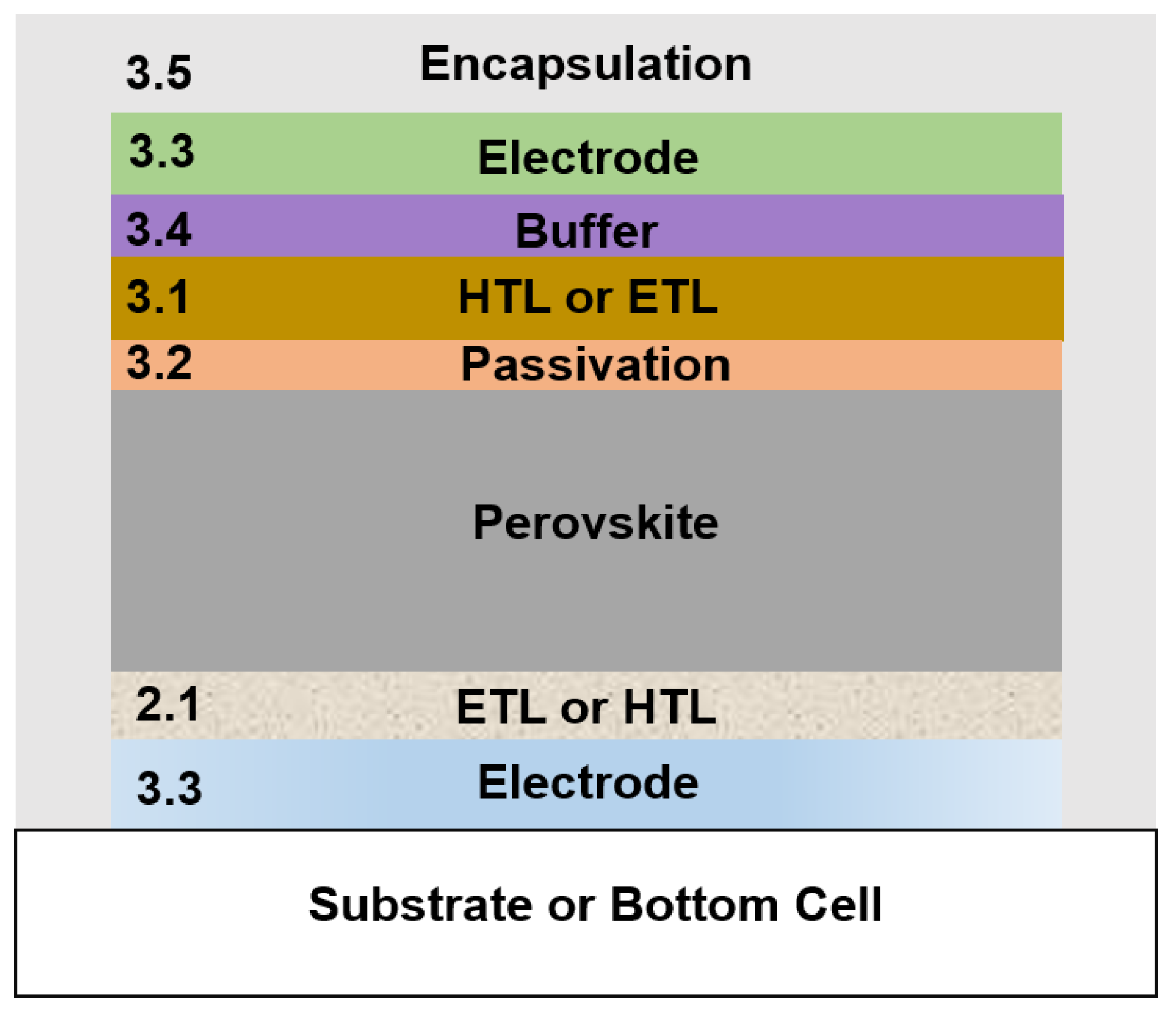
Figure 2.
Incorporation of atomic layer deposition (ALD) processes for SnO2 as electron transport layer (ETL): (a) Schematic of device configuration; (b) Cross-sectional scanning electron microscopy (SEM) image of the planar SnO2-based PSC (scale bar is 200 nm); (c) Illuminated current density vs. voltage scans for PSC with 15 nm of ALD SnO2. Reproduced from [24], with permission from the Royal Society of Chemistry, 2017. Incorporation of ALD processes for SnO2 as ETL in PSC with self-assembly monolayer (SAM) treatments: (d) Comparison of power conversion efficiency (PCE) between reverse and forward voltage scan for varying post-annealing and SAM treatments; (e) Illuminated current density vs. voltage (J–V) of optimal device. Reproducedfrom [25], with permission from Wiley, 2017. Incorporation of ALD processes for GaN as ETL in PSC: (f) Solar cell device configuration; (g) Cross-sectional SEM image of device. Reproduced from [30], with permission from the Royal Society of Chemistry, 2019.
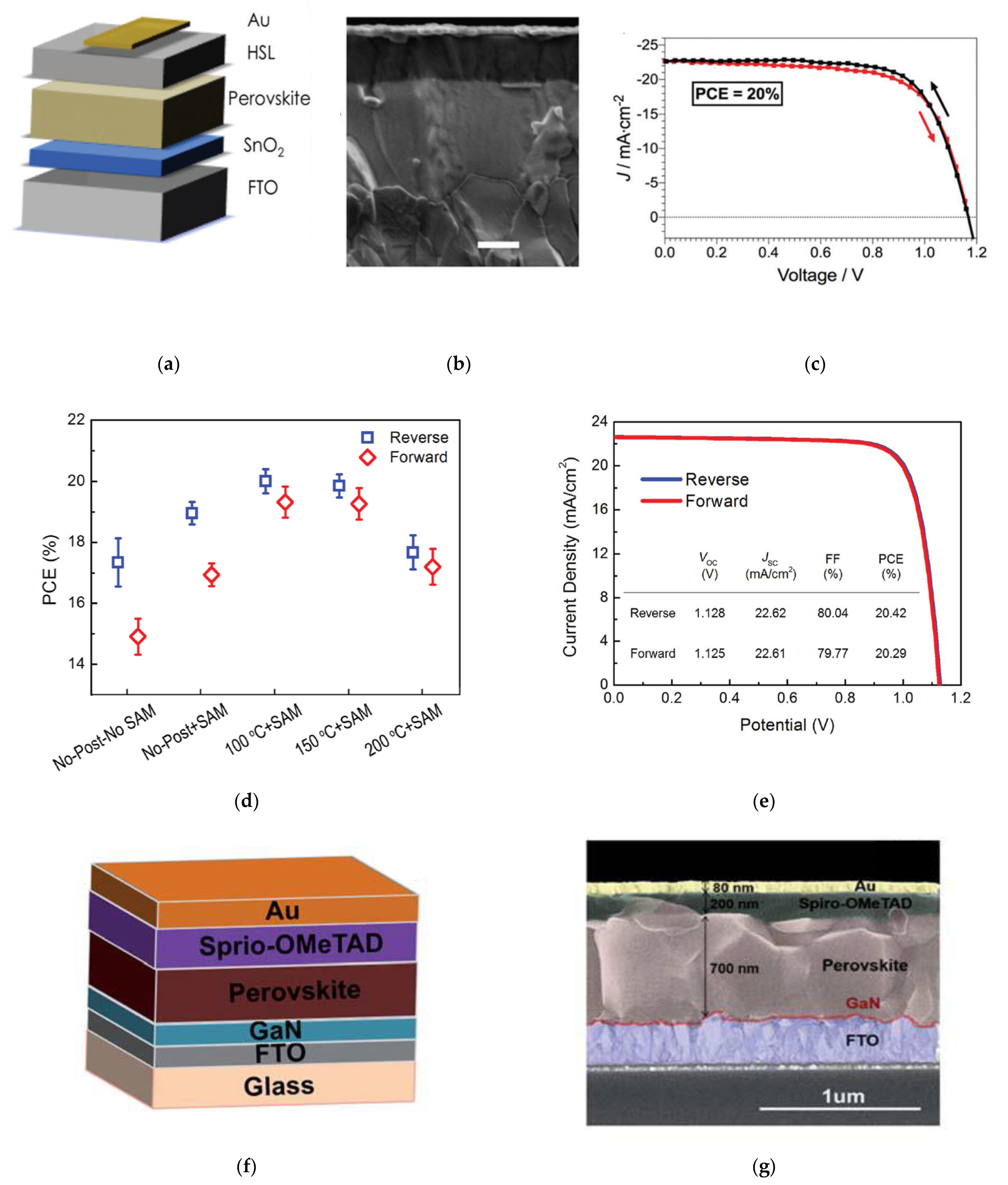
Figure 3.
Incorporation of ALD processes for NiO, TiO2, and aluminum-doped zinc oxide (AZO) in PSC: (a) Schematic of solar cell device stack and cross-sectional scanning electron microscopy image of the PSC device; (b) Illuminated J–V scans comparing PSCs with ALD TiO2 and ALD AZO. Reproduced from [47], with permission from Wiley, 2018. Incorporation of atmospheric pressure spatial ALD (s-ALD) processes for NiOx as hole transport layer (HTL) in PSC: (c) Cross-sectional SEM image of the PSC device; (d) Illuminated J–V scans comparing PSCs with the conventional HTL, poly(3,4-ethylenedioxythiophene) polystyrenesulfonate (PEDOT:PSS), and s-ALD NiOx (right). Reproduced from [45], with permission from the American Chemical Society, 2018. Incorporation of ALD processes for TiO2-IrOx as HTL in PSC: (e) Cross-sectional scanning electron microscopy image of PSC device; (f) Illuminated current density vs. voltage comparing PSCs with ALD TiO2-IrOx and nanoparticle NiO. Reproduced from [43], with permission from Wiley, 2018.
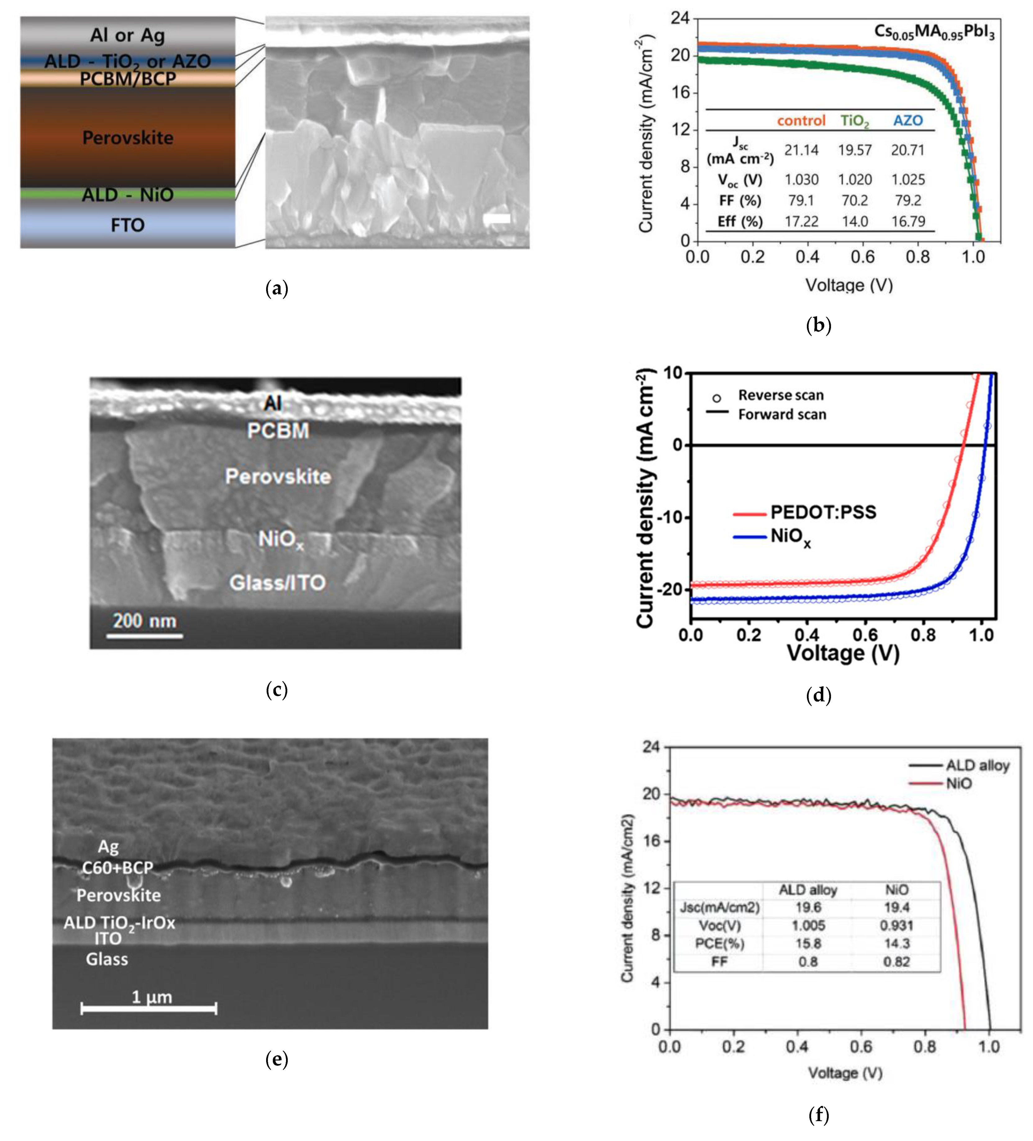
Figure 4.
Incorporation of ALD Al2O3 as passivation layer in PSC: (a) high angle annular dark field (HAADF) scanning transmission electron microscopy (TEM) image of the perovskite/Al2O3/spiro-OMeTAD interface, and the corresponding overlapping elemental mapping image; (b) Illuminated J-V scans comparing PSCs without and with Al2O3; (c) X-ray diffraction (XRD) scans of perovskite films without Al2O3; (d) X-ray diffraction (XRD) scans of perovskite films with Al2O3. Reproduced from [62], with permission from the Royal Society of Chemistry, 2017. Incorporation of ALD ZrO2 as barrier layer in PSC: (e) Illuminated current density vs. voltage comparing PSCs without and with the ALD Al2O3 barrier layer; (f) Illuminated current density vs. voltage comparing PSCs with ALD TiO2-IrOx and nanoparticle NiO. Reproduced from [74], with permission from Wiley, 2018.
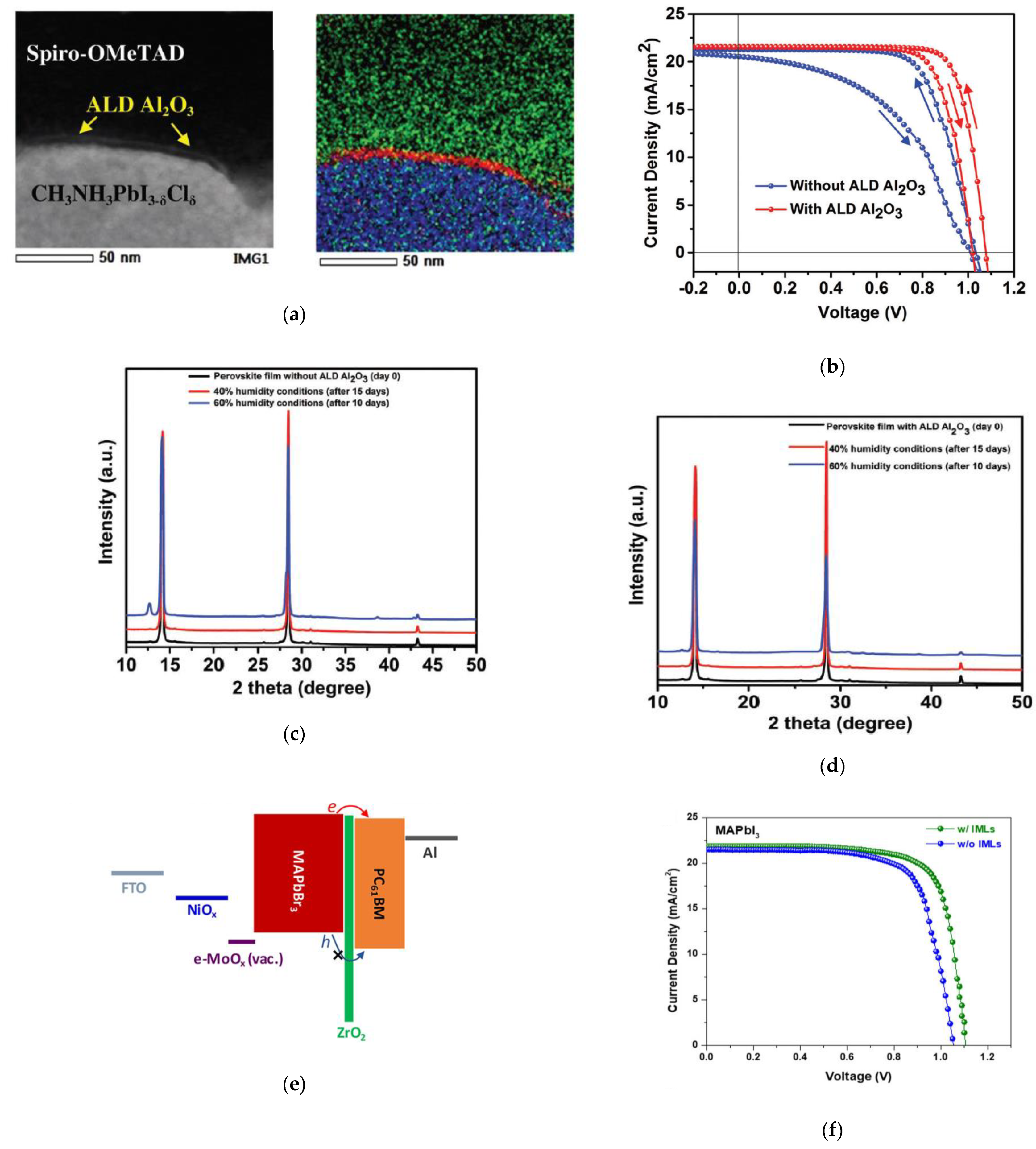
Figure 5.
Incorporation of ALD Ga2O3 as barrier layer between the ETL and top electrode in the PSC: (a) Schematic of the device configuration; (b) Illustration of degradation mechanism in the case without Ga2O3; (c) Illustration of the protection effect from degradation in the case with Ga2O3; (d) Normalized photovoltaic performance parameters as a function of ambient storage time for PSCs without Ga2O3; (e) Normalized photovoltaic performance parameters as a function of time for PSCs with Ga2O3. Reproduced from [65], with permission from Wiley, 2018.
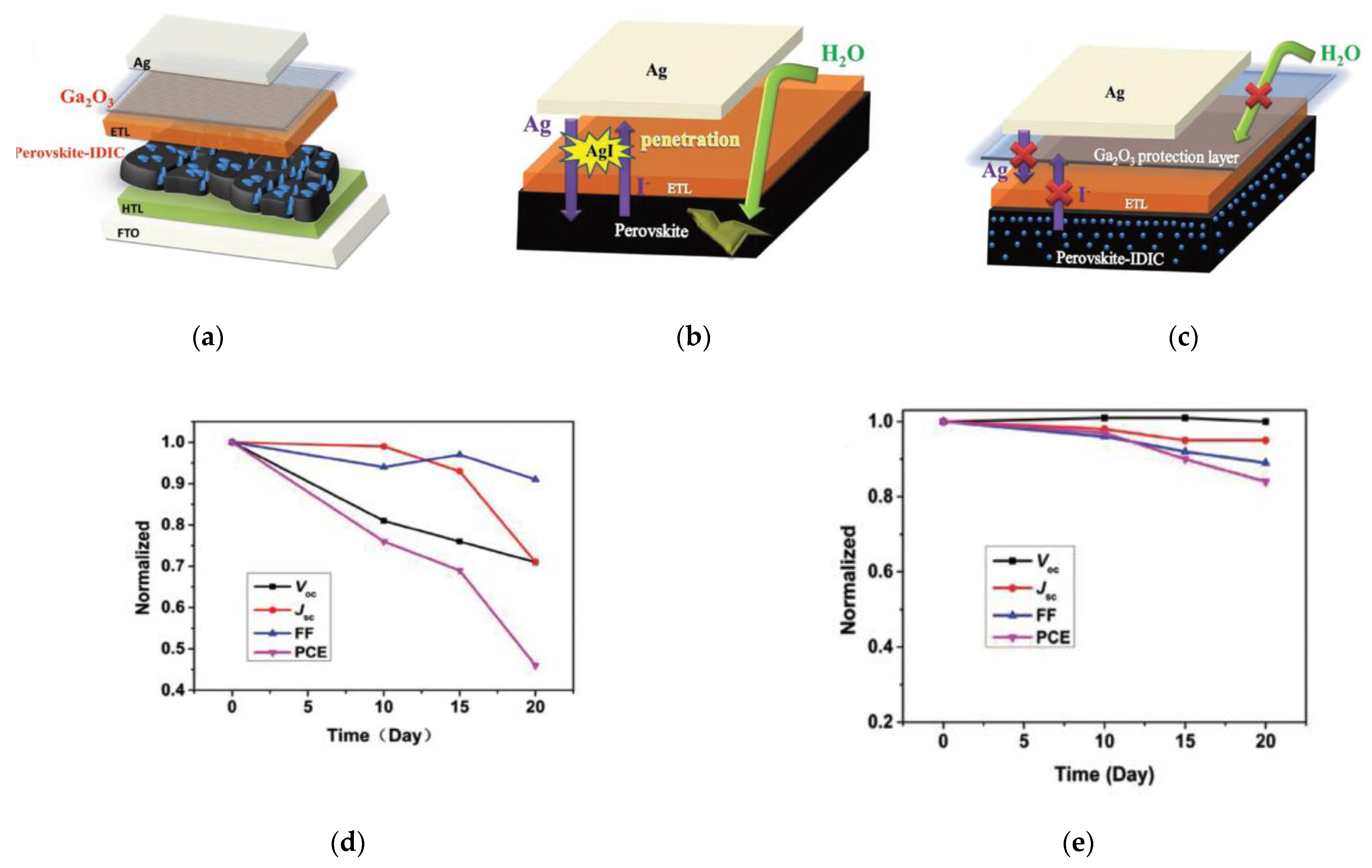
Figure 6.
Incorporation of ALD AZO as recombination layer in all-perovskite tandem solar cell: (a) Schematic of AZO without and with poly(ethylenimine) ethoxylated (PEIE) nucleation layer; (b) Cross-sectional SEM of solar cell stack; Reproduced from [63], with permission from Elsevier, 2019.
Figure 6.
Incorporation of ALD AZO as recombination layer in all-perovskite tandem solar cell: (a) Schematic of AZO without and with poly(ethylenimine) ethoxylated (PEIE) nucleation layer; (b) Cross-sectional SEM of solar cell stack; Reproduced from [63], with permission from Elsevier, 2019.

Figure 7.
Incorporation of ALD SnOx and zinc tin oxide (ZTO) in perovskite tandem devices: (a) Device stack configuration of the top perovskite cell; (b) Normalized PCE as a function of time for the various PSC devices. Reproduced from [59], with permission from the American Association for the Advancement of Science, 2019. Incorporation of atmospheric-pressure chemical vapor deposition (AP-CVD) of CuOx as a buffer layer in semitransparent PSC: (c) Schematic of band alignment of the device; (d) Cross-sectional SEM image of the device stack. Reproduced from [64], with permission from the American Chemical Society, 2020.


Table 1.
Summary of literature on ALD-grown layers below the absorber in perovskite solar cells.
| Material | Precursors | Temp. (°C) | Application/Structure | Device Stack | JSC (mA/cm2) | VOC (V) | FF (%) | η (%) | Institute, Year [Ref] |
|---|---|---|---|---|---|---|---|---|---|
| SnO2 | TDMASn + O3 | 118 | ETL/ n-i-p | FTO/SnO2 (15 nm)/FA0.85MA0.15Pb(I0.85Br0.15)3/spiro-OMeTAD/Au | 21.3 | 1.14 | 74.0 | 18.4 | EPFL, 2015 [31] |
| SnO2 | TDMASn + O3 | 100–120 | ETL/ n-i-p | FTO/d-TiO2/SnO2/FA0.85MA0.15Pb(I0.85Br0.15)3/PTAA/Au | 22.7 | 1.13 | 78.0 | 20.0 | EPFL, 2018 [32] |
| SnO2 | TDMASn + O3 | 118 | ETL/ n-i-p | FTO/SnO2 (15 nm)/Rb1(FA0.83MA0.17)99Pb(I0.83Br0.17)3/spiro-OMeTAD/Au | 23.0 | 1.17 | 71.0 | 20.0 | EPFL, 2017 [24] |
| SnO2 | TDMASn + O2 Plasma | 100 | ETL/ n-i-p | FTO/SnO2/100 °C/C60-SAM/FA0.30MA0.70PbI3/spiro-OMeTAD/Au | 22.6 | 1.13 | 80.0 | 20.4 | Toledo, 2017 [25] |
| SnO2 | TDMASn + O2 Plasma | 100 | ETL/ n-i-p | PET/ITO/SnO2/C60-SAM/FA0.30MA0.70PbI3/spiro-OMeTAD/Au | 22.1 | 1.10 | 75.4 | 18.4 | Toledo, 2017 [33] |
| SnO2 | TDMASn + O2 Plasma | 100 | ETL/ n-i-p | FTO/SnO2/C60-SAM/FA0.30MA0.70PbI3/spiro-OMeTAD/Au | 21.6 | 1.13 | 78.1 | 19.0 | Toledo, 2016 [34] |
| TiO2 | TiCl4 + H2O | 150 | ETL/ n-i-p | FTO/TiO2 (17 nm)/mp-TiO2/MAPbI3/Graphene Oxide/spiro-OMeTAD/Au | 20.2 | 1.04 | 73.0 | 15.1 | Tsinghua, 2014 [35] |
| TiO2 | TDMAT + H2O | 120 | ETL/ n-i-p | FTO/TiO2 (4 nm)/mp-TiO2/MAPbI3/spiro-OMeTAD/Au | 23.1 | 1.08 | 73.4 | 18.3 | Nanjing, 2018 [26] |
| TiO2 | TDMAT + H2O | 150 | ETL/ n-i-p | ITO/TiO2 (10 nm)/np-SnO2/PC61BM/FA0.30MA0.70Pb(I1-xClx)3/spiro-OMeTAD/Au | 23.0 | 1.08 | 78.2 | 19.5 | Xidian, 2019 [36] |
| TiO2 | TDMAT + H2O | 225 | ETL/ n-i-p | FTO/TiO2 (11 nm)/mp-TiO2/MAPbI3 | 22.3 | 1.11 | 74.0 | 18.4 | Tokyo, 2019 [37] |
| TiO2 | TDMAT + H2O | ETL/ n-i-p | FTO/mp-Sb:SnO2/TiO2 (10 nm)/MAPbI3/PTAA/Au | 23.8 | 1.10 | 77.0 | 20.1 | Soochow, 2018 [28] | |
| TiO2 | TDMAT + H2O | 120 | ETL, Passivation/ n-i-p | FTO/np-TiO2/TiO2 (2 nm)/MAPbI3/spiro-OMeTAD/Au | 17.6 | 0.97 | 67.0 | 11.5 | EPFL, 2014 [38] |
| TiO2 | TTIP + O2 Plasma | 130 | ETL/ n-i-p | ITO/CF4 plasma TiO2 (20 nm)/MAPbI3/spiro-OMeTAD/Au | 20.3 | 1.03 | 75.5 | 15.8 | Eindhoven, 2018 [39] |
| TiO2 | Ti(CpMe)(NMe2)3 + H2O | 150 | ETL Passivation/ n-i-p | ITO/ZnO (80 nm)/TiO2 (<3 nm)/Cs0.15FA0.75MA0.10PbI2.9Br0.1/spiro-OMeTAD/MoO3/Au | 22.5 | 1.03 | 74.0 | 17.1 | Soochow, 2018 [40] |
| TiO2 | TTIP + H2O | 250 | Passivation/n-i-p | FTO/c-TiO2/NR-TiO2/TiO2 (4 nm)/MAPbI3/spiro-OMeTAD/Au | 19.8 | 0.95 | 72.0 | 13.5 | CNU, 2015 [41] |
| TiN | TiCl4 + NH3 | 350 | ETL Passivation/ n-i-p | FTO/c-TiO2/mp-TiO2/TiN (<2 nm)/FA0.83MA0.17Pb(I0.83Br0.17)3/PTAA/Au | 22.5 | 1.14 | 75.0 | 19.0 | CNU, 2020 [42] |
| TiO2-IrOx | TDMAT + H2O (EtCp)Ir(CHD) + O3 | 175 | HTL/ p-i-n | ITO/TiO2-IrOx(10 nm)/Cs0.17FA0.83Pb(I0.83Br0.17)3/C60/BCP/Ag | 19.6 | 1.01 | 80.0 | 15.8 | Stanford, 2018 [43] |
| GaN | TEG + Ar/N2/H2 plasma | 280 | ETL/ n-i-p | FTO/GaN (5 nm)/FA0.85MA0.15Pb(I0.85Br0.15)3/spiro-OMeTAD/Au | 22.6 | 0.98 | 68.9 | 15.2 | UST Beijing, 2019 [30] |
| HfO2 | TEMAHf + H2O | 90 | Passivation/ n-i-p | PEN/ITO/HfO2 (<1 nm)/SnO2/Cs0.05(FA0.83MA0.17)0.95Pb(I0.83Br0.17)3 + RbI + KI/spiro-OMeTAD/Au | 21.2 | 1.14 | 79.2 | 19.1 | Xiamen, 2019 [44] |
| Nb2O5 | (tert-butylimido)bis(diethylamino)niobium + O3 | 170 | ETL/ n-i-p | FTO/Nb2O5 (15 nm)/FA0.85MA0.15Pb(I0.85Br0.15)3/spiro-OMeTAD/Au | Very low | EPFL, 2015 [31] | |||
| NiO | Ni(MeCp)2 + O2 | 350 | HTL/ p-i-n | ITO/s-ALD NiOx/FA0.2MA0.8PbI3/PC61BM/Al | 23.0 | 1.08 | 81.0 | 17.1 | Cambridge, 2018 [45] |
| NiO | Ni(MeCp)2 + O2 plasma | 150 | HTL/ p-i-n | ITO/NiO (10 nm)/Cs0.05(FA0.83MA0.17)Pb(I0.83Br0.17)3/C60/BCP/Cu | 21.8 | 1.07 | 73.4 | 17.1 | Eindhoven, 2019 [46] |
| NiO, AZO, Al2O3 | Ni(dmamb)2 + O3, TMA/DEZ + H2O | 200, 100, 100 | ETL/ p-i-n | FTO/NiO (6 nm)/Cs0.05MA0.95PbI3/PCBM/BCP/AZO (40 nm)/Ag/Al2O3 (50 nm) | 22.5 | 1.03 | 80.8 | 18.8 | SKKU, 2018 [47] |
| VOx | V(dma)4 + H2O | 50 | HTL/ p-i-n | ITO/VOx (1 nm)/MAPbI3/PC61BM/BCP/Ag | 17.9 | 0.90 | 71.2 | 11.5 | Peking, 2018 [48] |
| ZnO/Al2O3 | DEZ + H2O | 150 | ETL/ n-i-p | FTO/ZnO (50 nm)/Al2O3 (<1 nm)/mp-TiO2/MAPbI3/spiro-OMeTAD/Au | 18.9 | 1.01 | 62.0 | 15.6 | UST Beijing, 2016 [49] |
| ZnS | DEZ + H2S | 150 | Passivation/ n-i-p | FTO/c-TiO2/mp-TiO2/ZnS (<2 nm)/FA0.85MA0.15Pb(I0.85Br0.15)3/PTAA/Au | 22.5 | 1.13 | 75.0 | 18.8 | CNU, 2020 [29] |
Table 2.
Summary of literature on ALD-grown layers above the absorber in perovskite solar cells.
| Material | Precursors | Temp. (°C) | Application/Structure | Device Stack | JSC (mA/cm2) | VOC (V) | FF (%) | η (%) | Institute, Year [Ref] |
|---|---|---|---|---|---|---|---|---|---|
| Al2O3 | TMA + H2O | 100 | Passivation/ n-i-p | ITO/c-TiO2/MAPb(I1-xClx)3/Al2O3 (1 nm)/spiro-OMeTAD/Au | 21.7 | 1.07 | 77.0 | 18.0 | Eindhoven, 2017 [62] |
| NiO, AZO, Al2O3 | Ni(dmamb)2 + O3, TMA/DEZ + H2O | 200, 100, 100 | ETL/ p-i-n | FTO/NiO (6 nm)/Cs0.05MA0.95PbI3/PCBM/BCP/AZO (40 nm)/Ag/Al2O3 (50 nm) | 22.5 | 1.03 | 80.8 | 18.8 | SKKU, 2018 [47] |
| AZO | TMA/DEZ + H2O | 85 | Recombination/ p-i-n | ITO/PolyTPD/PFN/Cs0.30FA0.60MA0.10Pb(I0.80Br0.20)3/LiF/C60/PEIE/AZO (25 nm)/IZO/PEDOT:PSS/Cs0.25FA0.75Sn0.5Pb0.5I3/C60/BCP/Au | 15.6 | 1.82 | 75.0 | 21.3 | NREL, 2019 [63] |
| CuOx | Cu(dmamb)2 + H2O | 100 | Buffer/ n-i-p (ST) | FTO/c-TiO2/mp-TiO2/FA0.95MA0.05Pb(I0.95Br0.05)3/PTAA/pulsed-CVD CuOx (15 nm)/ITO | 21.7 | 1.01 | 71.1 | 15.6 | KRICT, 2020 [60] |
| CuOx | ATHFAACu + H2O | 100 | Buffer/ n-i-p (ST) | FTO/c-TiO2/mp-TiO2/Cs0.05(MA0.17FA0.83)0.95Pb(I0.83Br0.17)3/PTAA/AP-CVD CuOx (3 nm)/ITO/MgF2 | 20.6 | 1.10 | 73.7 | 16.7 | Cambridge, 2020 [64] |
| Ga2O3 | Ga2(NMe2)6 + H2O | 120 | Passivation/ p-i-n | FTO/Li:NiO/MAPbI3/IDIC/PCBM/BCP/Ga2O3 (<2 nm)/Ag | 22.4 | 1.12 | 79.4 | 19.9 | Wuhan, 2018 [65] |
| SnO2 | TDMASn + H2O | 100 | Buffer/ p-i-n (2-T) | Si PV/ITO/PTAA/Cs0.15(FA0.83MA0.17)0.85Pb(I0.7Br0.3)3/ICBA/C60/SnO2/IZO/MgF2 | 17.8 | 1.80 | 79.4 | 25.4 | UNC, 2019 [66] |
| SnO2 | TDMASn + H2O | 100 | Buffer/ p-i-n (2-T) | Si PV/spiro-TTB/CsxFA1-xPb(I1-yBry)3/LiF/C60/SnO2/IZO/MgF2 | 19.5 | 1.74 | 74.7 | 25.4 | EPFL, 2019 [67] |
| SnO2 | TDMASn + H2O | Buffer/ p-i-n (2-T) | Si PV/ITO/PTAA/Cs0.05(FA0.83MA0.17)0.95Pb(I0.83Br0.17)3/C60/SnO2 (20 nm)/IZO/AR foil | 18.5 | 1.76 | 78.5 | 25.5 | HZB, 2018 [68] | |
| SnOx/Zn:SnOx | TDMASn/DEZ + H2O | 85 | Buffer/ p-i-n (ST) | ITO/PTAA/Cs0.05FA0.80MA0.15Pb (I0.85Br0.15)3/C60/BCP/SnOx (6 nm)/Zn:SnOx (2 nm)/IZO | 20.8 | 1.12 | 79.3 | 18.5 | NREL, 2019 [59] |
| SnO2/Zn:SnOx | TDMASn/DEZ + H2O | 85 | Buffer/ p-i-n (ST) | ITO/PTAA/Cs0.15FA0.65MA0.20Pb (I0.80Br0.20)3 + PEAI + Pb(SCN)2/C60/SnOx (6 nm)/Zn:SnOx (2 nm)/IZO | 19.6 | 1.14 | 76.8 | 17.1 | NREL, 2019 [69] |
| SnO2/Zn:SnOx | TDMASn/DEZ + H2O | 90 | ETL/ p-i-n | ITO/Poly-TPD/PFN/Cs0.25FA0.75Pb(I0.80Br0.20)3/LiF/C60/PEIE/SnO2/Zn:SnOx/Au | 19.7 | 1.15 | 81.8 | 18.6 | Stanford, 2019 [70] |
| TiO2 | TDMAT + H2O | 60 | ETL/ p-i-n | ITO/NiO/MAPbI3/PC61BM (40 nm)/TiO2 (2 nm)/Ag | 22.8 | 1.04 | 76.9 | 18.3 | Nanjing, 2018 [71] |
| VOx | VTIP + H2O | 80 | Buffer/ n-i-p (ST) | ITO/np-SnO2/C60/FA0.83MA0.17Pb(I0.83Br0.17)3/spiro-TTB/VOx (9 nm)/ITO | 18.9 | 1.07 | 71.0 | 14.2 | Stanford, 2019 [72] |
| ZnO | DEZ + H2O | 80 | ETL/ p-i-n | ITO/PEDOT:PSS/MAPbI3/ZnO (40 nm)/Ag NWs/ALD Al2O3 (50 nm)-coated PET | 20.7 | 1.02 | 76.4 | 16.2 | Feng Chia, 2015 [73] |
| ZrO2 | TDMAZr + O3 | 80 | Passivation/ p-i-n | FTO/NiOx/e-MoOx (10 nm)/MAPbI3/ZrO2 (<2 nm)/PC61BM/Al | 21.9 | 1.11 | 75.0 | 18.2 | SCN, 2018 [74] |
Table 3.
Summary of advantages and disadvantages of conventional ALD and its variations.
| Deposition Method | Advantages | Disadvantages |
|---|---|---|
| Conventional ALD |
|
|
| Pulsed-CVD |
|
|
| Spatial ALD |
|
|
Publisher’s Note: MDPI stays neutral with regard to jurisdictional claims in published maps and institutional affiliations. |
© 2021 by the author. Licensee MDPI, Basel, Switzerland. This article is an open access article distributed under the terms and conditions of the Creative Commons Attribution (CC BY) license (http://creativecommons.org/licenses/by/4.0/).
Share and Cite
MDPI and ACS Style
Park, H.H. Inorganic Materials by Atomic Layer Deposition for Perovskite Solar Cells. Nanomaterials 2021, 11, 88. https://doi.org/10.3390/nano11010088
AMA Style
Park HH. Inorganic Materials by Atomic Layer Deposition for Perovskite Solar Cells. Nanomaterials. 2021; 11(1):88. https://doi.org/10.3390/nano11010088
Chicago/Turabian StylePark, Helen Hejin. 2021. "Inorganic Materials by Atomic Layer Deposition for Perovskite Solar Cells" Nanomaterials 11, no. 1: 88. https://doi.org/10.3390/nano11010088
Note that from the first issue of 2016, this journal uses article numbers instead of page numbers. See further details here.