
Progress in THz Rectifier Technology: Research and Perspectives


Abstract
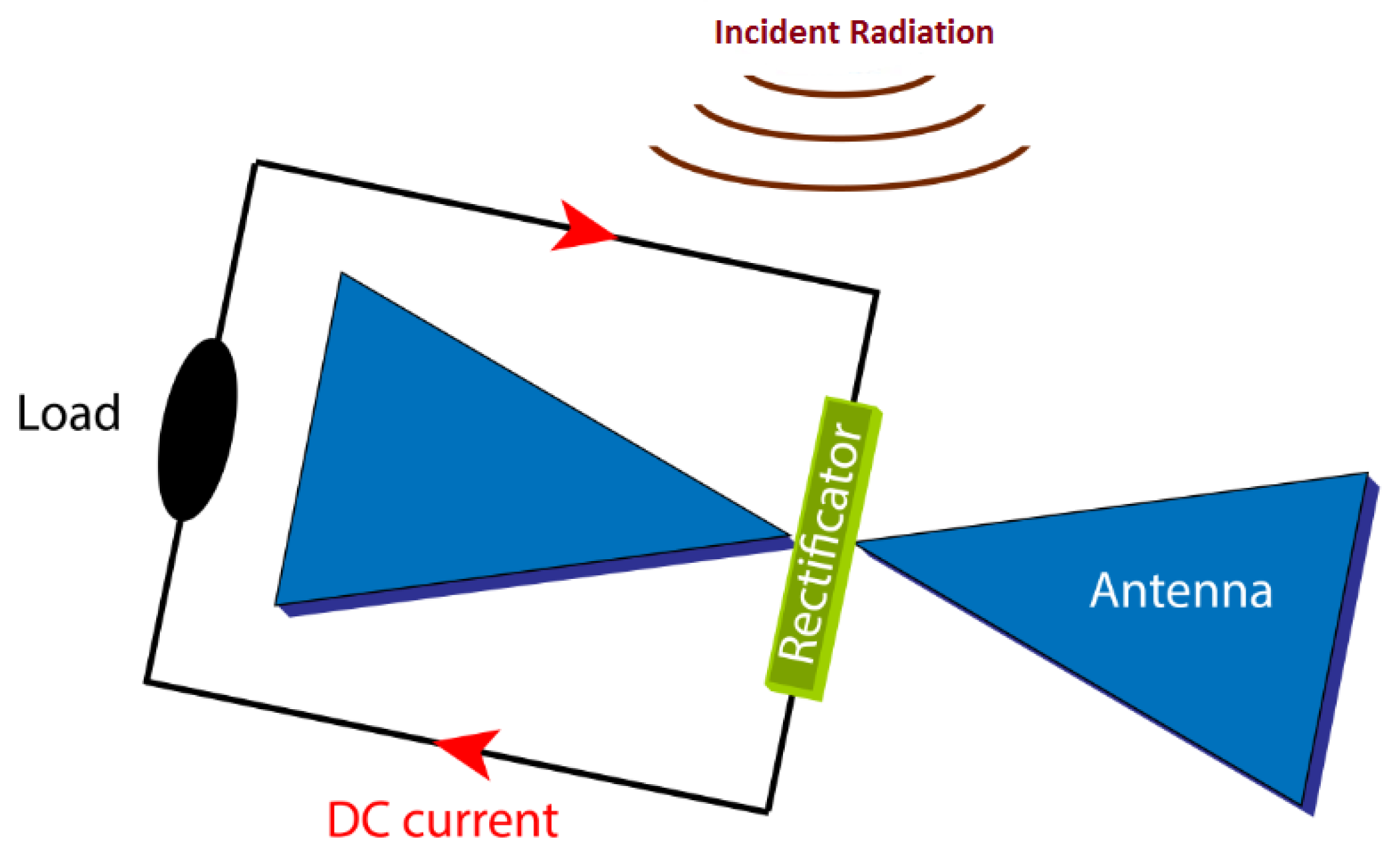
:1. Introduction
Rectification Efficiency (η)
- -
- is the efficiency of the coupling between the incident EM radiation and the antenna.
- -
- is the efficiency given by the ratio between the energy transmitted to the nanodiode and the energy collected by the nanoantenna.
- -
- is the coupling efficiency between the nanoantenna and the rectifier.
- -
- is the efficiency given by the ratio between the rectified power and the power received by the nanodiode.
2. THz Diode Technology: General Information, FOMs, Open Questions, State of the Art, and Perspectives
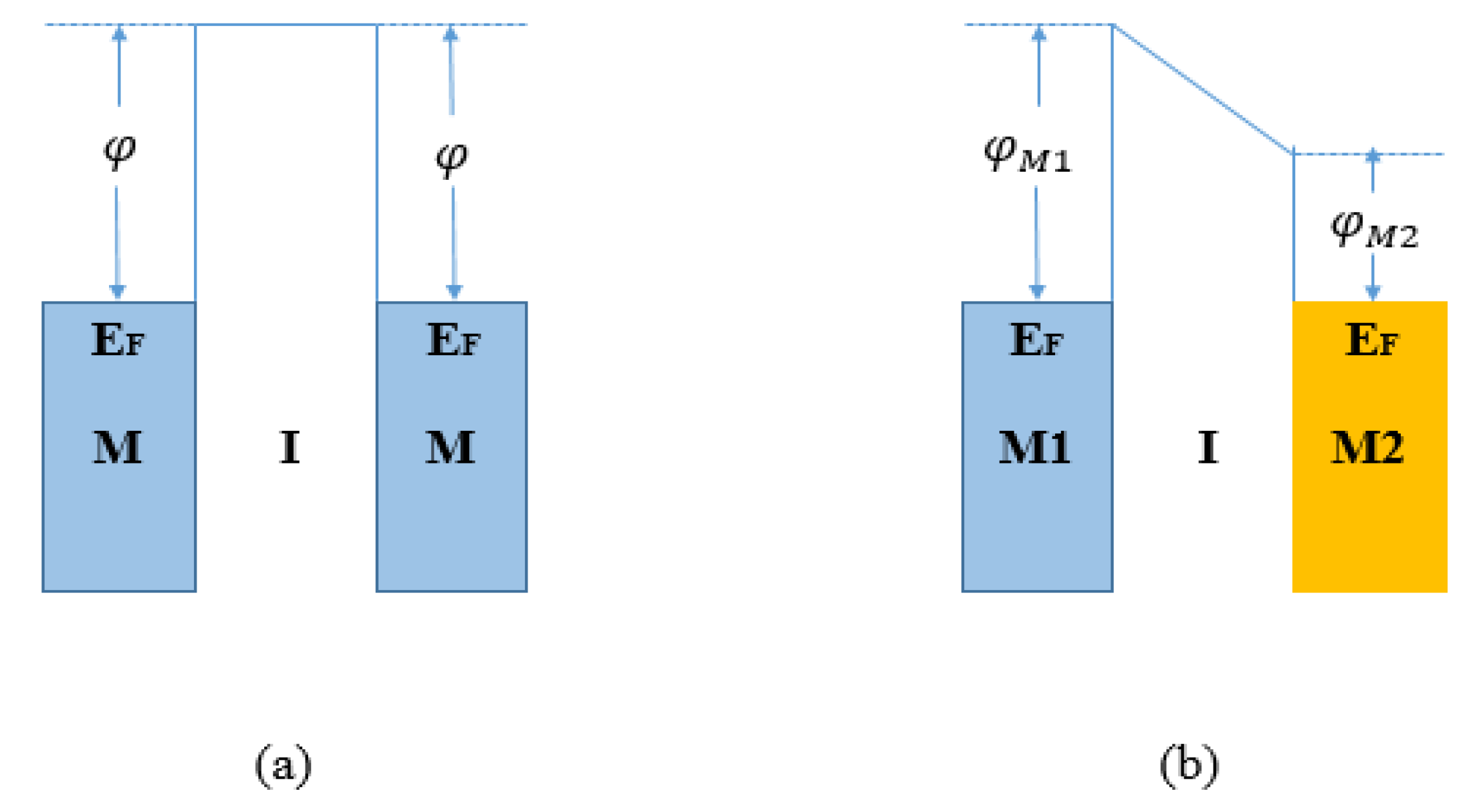
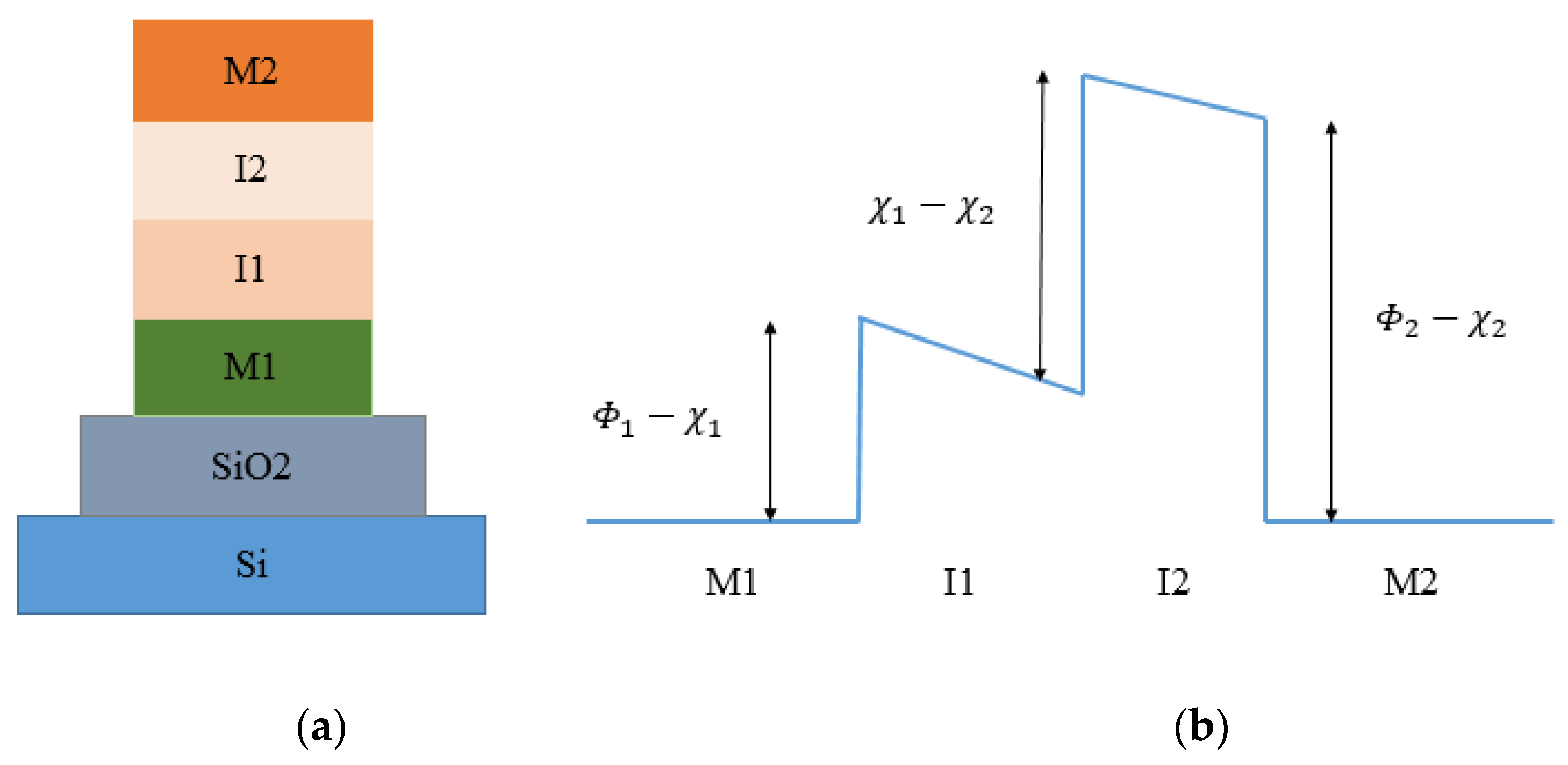
2.1. THz Diode Technology: General Information on Metal Insulator Metal (MIM) Diode
2.2. THz Diode Technology: I-V Characteristics and Figures of Merit (FOM) for MIM Diode
2.2.1. Current Density
2.2.2. Transmission Probability D
2.2.3. Turn-On Voltage (TOV)
2.2.4. Zero-Bias Resistance (ZBR)
2.2.5. Asymmetry (Asym)
2.2.6. Nonlinearity (NL)
2.2.7. Responsivity (S)
2.3. THz Diode Technology: Open Questions
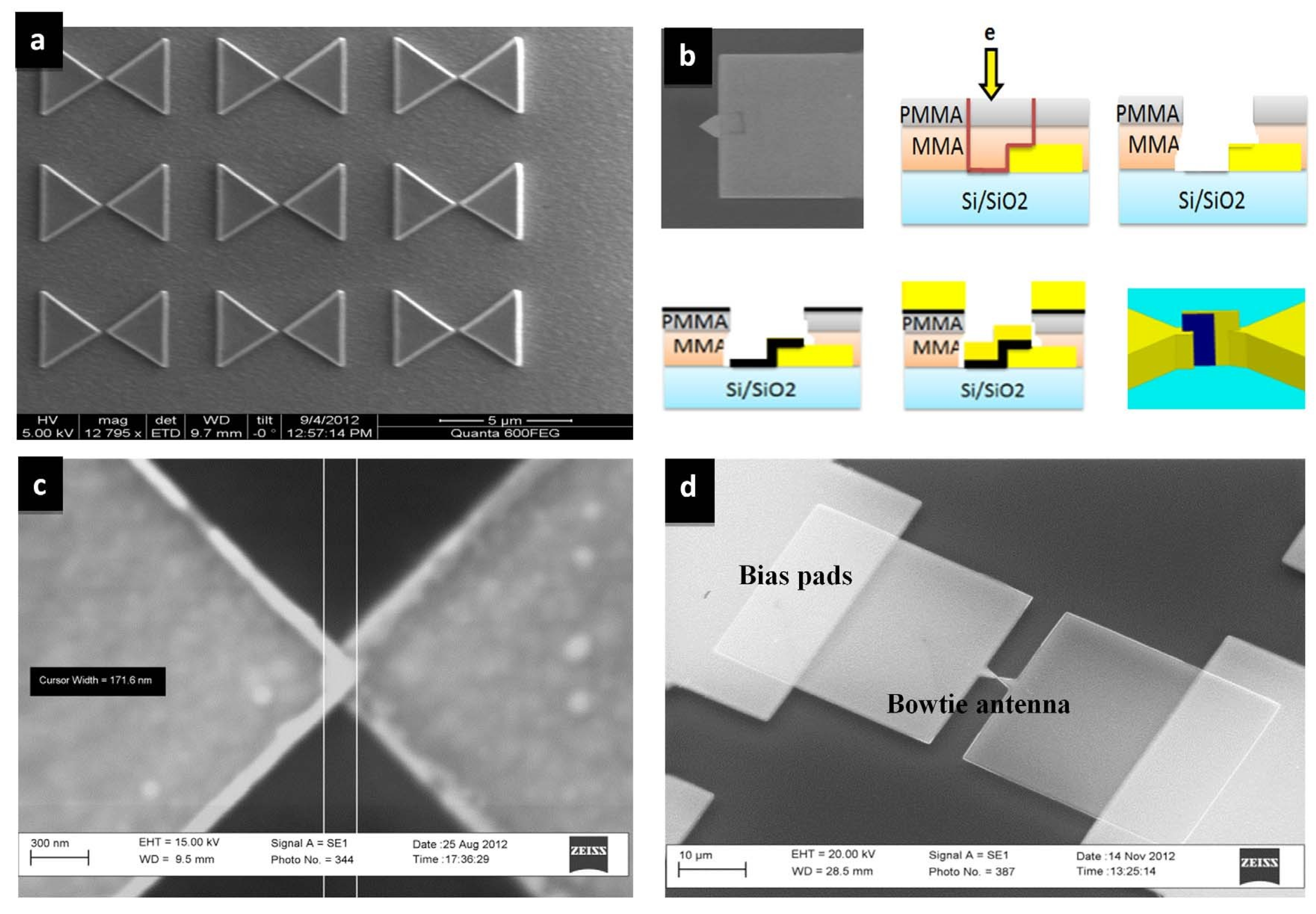
2.4. THz Diode Technology: State of the Art of Metal Insulator Metal (MIM) Diode
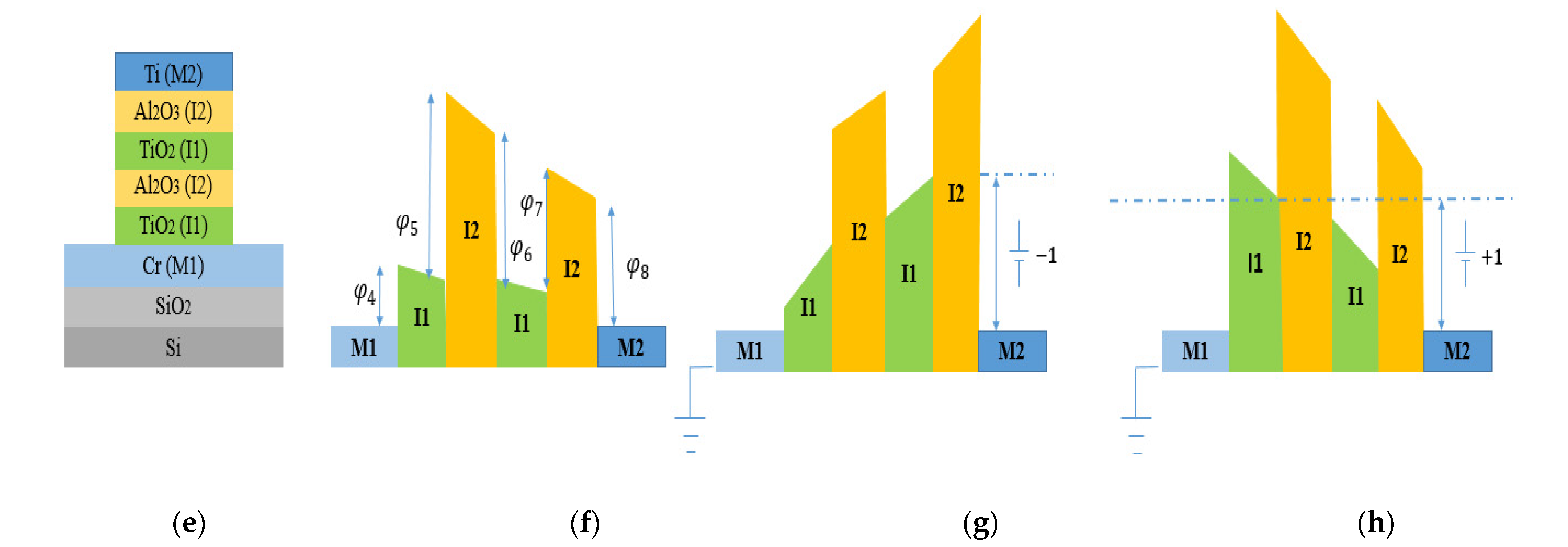
2.5. THz Diode Technology: General Information on Metal Multi-Insulator Metal (MInM) Diode
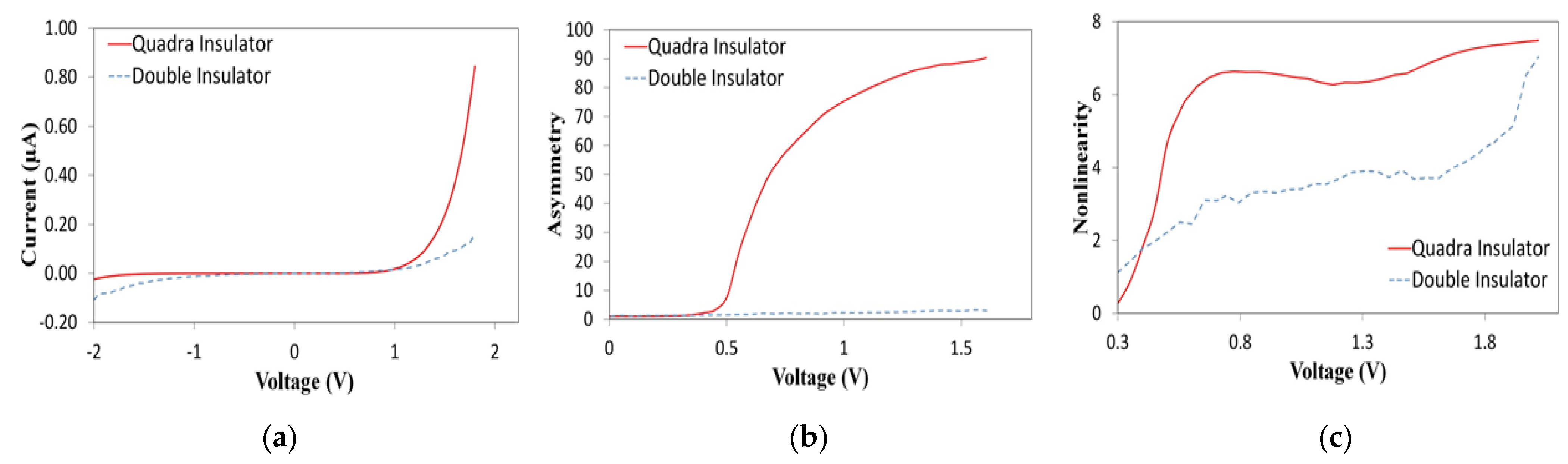
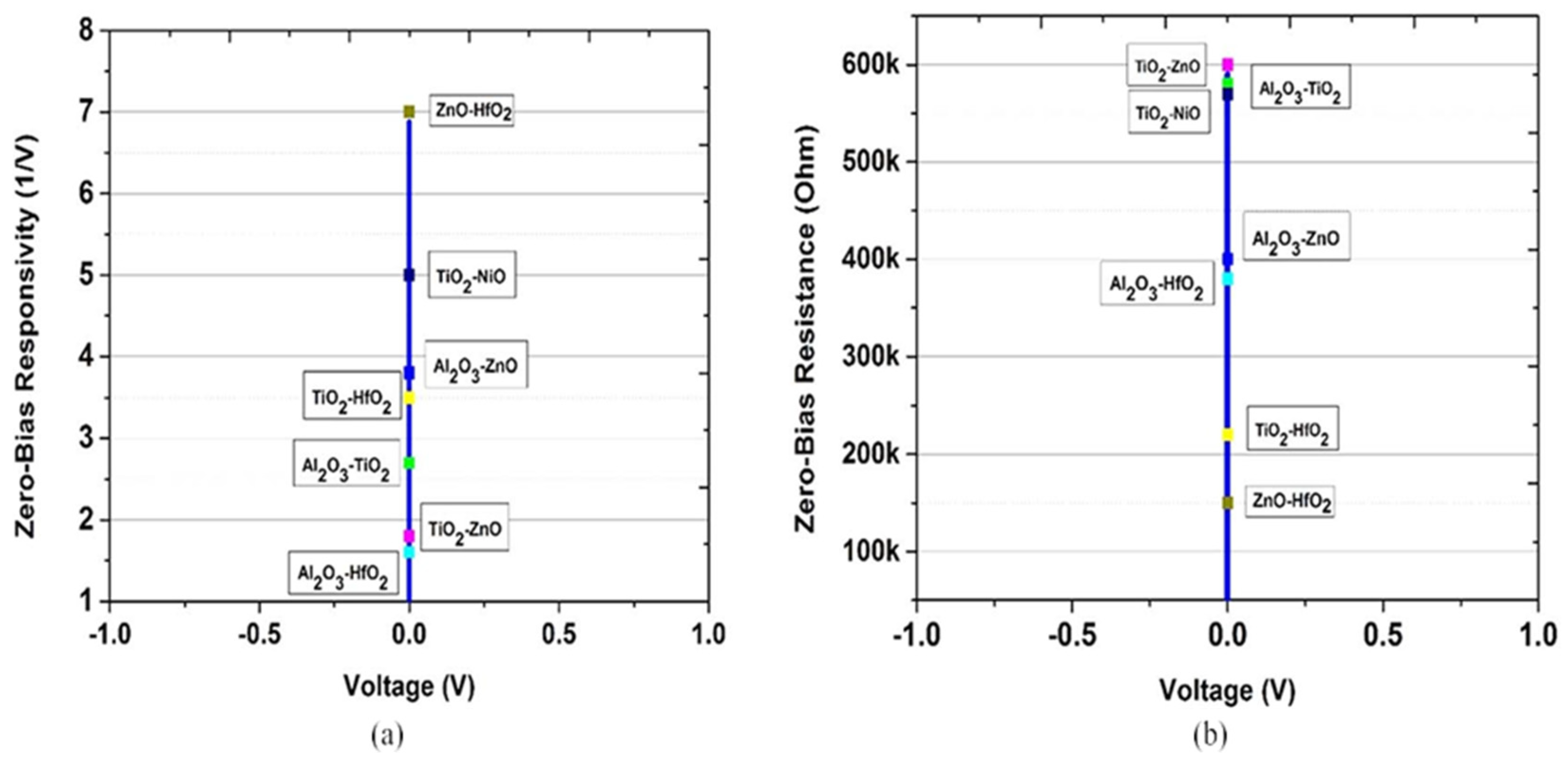
2.6. THz Diode Technology: State of the Art on Metal Multi-Insulator Metal (MInM) Diode
3. THz Diode Technology: General Information on Geometric Diode (GD)
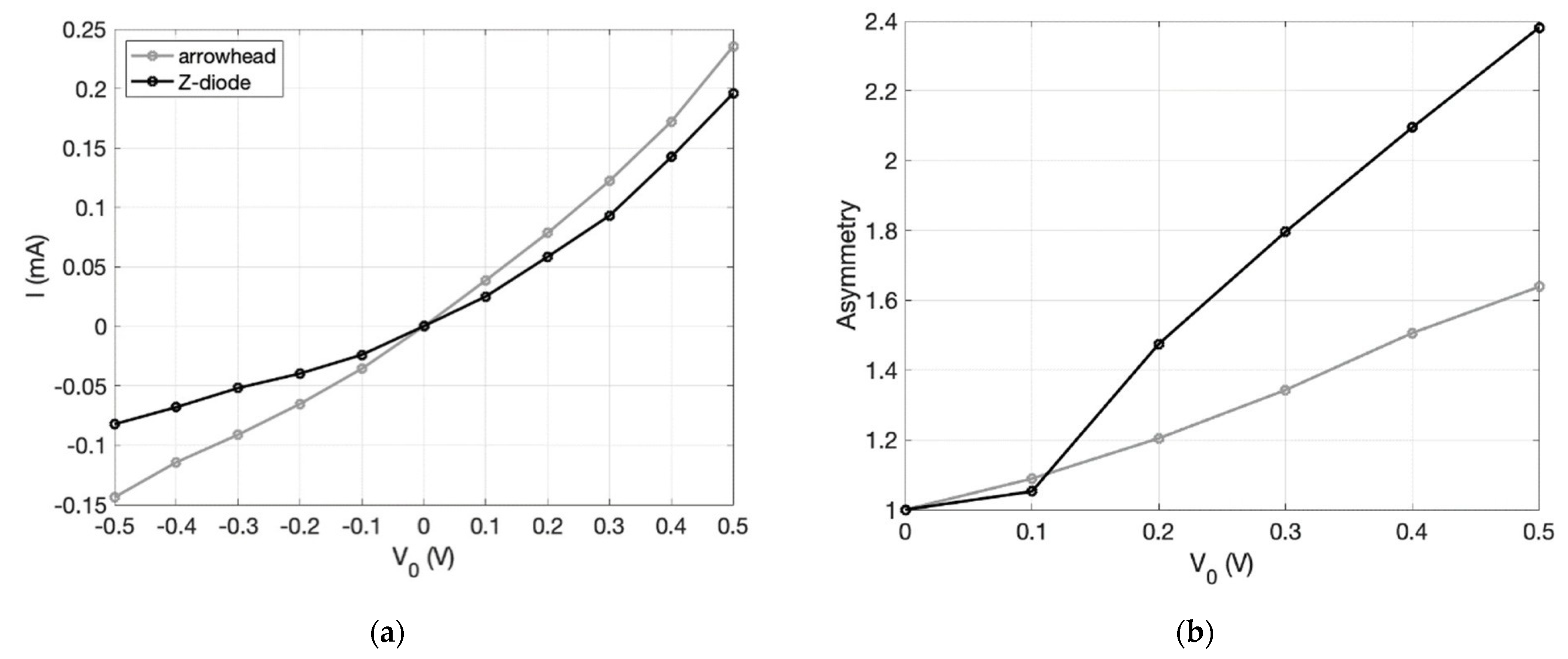
THz Diode Technology: State of the Art on Geometric Diode (GD)
4. Perspectives in THz Rectifier Technology for Energy Harvesting Applications
4.1. MIM and MInM Diodes
4.2. Geometric Diode (GD)
5. Conclusions
Author Contributions
Funding
Institutional Review Board Statement
Informed Consent Statement
Data Availability Statement
Acknowledgments
Conflicts of Interest
Abbreviations
| IR | Infrared |
| THz | Terahertz |
| DC | direct current |
| EH | energy harvesting |
| Si | Silicon |
| S&Q | Shockley–Queisser |
| EM | electromagnetic |
| Rectifying antenna | Rectenna |
| SPPs | Surface Plasmon Polaritons |
| E | electric field |
| AC | alternating current |
| LPF | Low pass filter |
| Overall efficiency | |
| Antenna collection efficiency | |
| Losses in the material | |
| Coupling or matching efficiency | |
| Antenna resistance | |
| Diode resistance | |
| Diode capacitance | |
| ω | Operating frequency |
| Quantum efficiency | |
| MIM | Metal-Insulator-Metal |
| MInM | Metal- multi-insulator-Metal |
| GD | geometric diode |
| Cut-off frequency | |
| EBL | electron beam lithography |
| MBE | molecular beam epitaxy |
| SEM | scanning electron microscopy |
| MOCVD | metalorganic chemical vapor deposition |
| PR | Photoresist |
| ICP | inductively coupled plasma |
| TMAH | tetramethylammonium hydroxide |
| PECVD | plasma-enhanced chemical vapor deposition |
| FOMs | Figure of Merits |
| Ψ | Work function |
| χ | Electron affinity |
| φ | Barrier height |
| Δφ | Barrier width |
| EF | Fermi levels |
| DT | direct tunneling |
| FNT | Fowler–Nordheim Tunneling |
| I-V | current to voltage |
| TOV | Turn-on voltage |
| ZBR | zero-bias resistivity |
| Sym | Symmetry |
| Asym | Asymmetry |
| NL | Nonlinearity |
| S | Responsivity |
| RC | Resistance-Capacitance |
| BG | Band gap |
| H-BN | hexagonal Boron Nitride |
| MIG | Metal-insulator-graphene |
| Gr-h-BN-Gr | graphene/hexagonal boron nitride (h-BN)/graphene heterostructure |
| ALD | atomic layer deposition |
| GBG-TD | graphene/h-BN/graphene tunneling diode |
| CVD | chemical vapor deposition |
| GrIM | Graphene-Oxide-Metal Diode |
| AAO | Anodic Aluminum Oxide |
| AP-CVD | atmospheric pressure chemical vapor deposition |
| PEALD | Plasma-enhanced atomic layer deposition |
| PMMA | polymethyl methacrylate |
| MIBK: IPA | methyl-isobutyl ketone: isopropanol |
| PVD | Physical Vapor Deposition |
| MIIM | metal-insulator-insulator-metal |
| M-I | Metal-interface |
| I-I | Interface-Interface |
| I-M | Interface-metal |
| QW | Quantum Well |
| MI2M | Metal-insulator-insulator-metal |
| MI4M | metal-insulator-insulator-insulator-insulator-metal |
| IPA | Isopropanol alcohol |
| MI3M | metal-insulator-insulator-insulator-metal |
| TEM | transmission electron microscope |
| MFPL | mean-free path length |
| AFM | atomic force microscopy |
| dn | neck width |
| ds | Shoulder width |
| TaN | Tantalum nitride |
References
- Citroni, R.; Di Paolo, F.; Livreri, P. Evaluation of an optical energy harvester for SHM application. Int. J. Electron. Commun. (AEÜ) 2019, 111, 152918. [Google Scholar] [CrossRef]
- Citroni, R.; Di Paolo, F.; Livreri, P. A Novel Energy Harvester for Powering Small UAVs: Performance Analysis, Model Validation and Flight Results. Sensors 2019, 19, 1771. [Google Scholar] [CrossRef] [PubMed] [Green Version]
- Byrness, S.J.; Blanchard, R.; Capasso, F. Harvesting renewable energy from Earth’s mid-infrared emissions. Proc. Natl. Acad. Sci. USA 2014, 111, 3927–3932. [Google Scholar] [CrossRef] [PubMed] [Green Version]
- Hemour, S.; Wu, K. Radio-Frequency Rectifier for Electromagnetic Energy Harvesting: Development Path and Future Outlook. Proc. IEEE 2014, 102, 1667–1691. [Google Scholar] [CrossRef]
- Bean, J.A.; Weeks, A.; Boreman, G.D. Performance Optimization of Antenna-Coupled Al/AlOx/Pt Tunnel Diode Infrared Detectors. IEEE J. Quantum Electron. 2011, 47, 126–135. [Google Scholar] [CrossRef]
- Mupparapu, R.; Cunha, J.; Tantussi, F.; Jacassi, A.; Summerer, L.; Patrini, M.; Giugni, A.; Maserati, L.; Alabastri, A.; Garoli, D.; et al. High-Frequency Light Rectification by Nanoscale Plasmonic Conical Antenna in Point-Contact-Insulator-Metal Architecture. Adv. Energy Mater. 2022, 12, 2103785. [Google Scholar] [CrossRef]
- Donchev, E.; Pang, J.S.; Gammon, P.M.; Centeno, A.; Xie, F.; Petrov, P.K.; Breeze, J.D.; Ryan, M.P.; Riley, D.J.; Alford, N.M. The rectenna device: From theory to practice (a review). MRS Energy Sustain. Rev. J. 2014, 1, E1. [Google Scholar] [CrossRef] [Green Version]
- Gadalla, M.N.; Abdel-Rahman, M.; Shamim, A. Design, optimization and fabrication of a 28.3 THz nano-rectenna for infrared detection and rectification. Sci. Rep. 2014, 4, 4270. [Google Scholar] [CrossRef]
- Davids, P.S.; Jarecki, R.L.; Starbuck, A.; Burckel, D.B.; Kadlec, E.A.; Ribaudo, T.; Shaner, E.A.; Peters, D.W. Infrared rectification in a nanoantenna-coupled metal-oxide-semiconductor tunnel diode. Nat. Nanotechnol. 2015, 10, 1033–1038. [Google Scholar] [CrossRef]
- Amara, W.; Yahyaoui, A.; Eltresy, N.; Aseeri, M.; Hakim, B.; Al-Turki, Y.; Rmili, H. Vivaldi dipole nano-rectenna for IR energy harvesting at 28.3 THz. Int. J. Numer. Model. 2021, 34, e2836. [Google Scholar] [CrossRef]
- Davids, P.S.; Kirsch, J.; Starbuck, A.; Jarecki, R.; Peters, S.D. Electrical power generation from moderate-temperature radiative thermal sources. Science 2020, 367, 1341–1345. [Google Scholar] [CrossRef] [PubMed]
- Weerakkody, A.; Belkadi, A.; Moddel, G. Nonstoichiometric Nanolayered Ni/NiO/Al2O3/CrAu Metal–Insulator–Metal Infrared Rectenna. ACS Appl. Nano Mater. 2021, 4, 2470–2475. [Google Scholar] [CrossRef]
- Belkadi, A.; Weerakkody, A.; Moddel, G. Demonstration of resonant tunneling effects in metal-double-insulator-metal (MI2M) diodes. Nat. Commun. 2021, 12, 2925. [Google Scholar] [CrossRef] [PubMed]
- Dragoman, M.; Aldrigo, M. Graphene rectenna for efficient energy harvesting at terahertz frequencies. Appl. Phys. Lett. 2016, 109, 113105. [Google Scholar] [CrossRef]
- Hemmetter, A.; Yang, X.; Wang, Z.; Otto, M.; Uzlu, B.; Andree, M.; Pfeiffer, U.; Vorobiev, A.; Stake, J.; Lemme, M.C.; et al. Terahertz Rectennas on Flexible Substrates Based on One-Dimensional Metal–Insulator–Graphene Diodes. ACS Appl. Electron. Mater. 2021, 3, 3747–3753. [Google Scholar] [CrossRef]
- Sharma, A.; Singh, V.; Bougher, T.L.; Cola, B.A. A carbon nanotube optical rectenna. Nat. Nanotechnol. 2015, 10, 1027–1032. [Google Scholar] [CrossRef] [PubMed]
- Anderson, E.C.; Bougher, T.L.; Cola, B.A. High performance multiwall carbon nanotube–insulator–metal tunnel diode arrays for optical rectification. Adv. Electron. Mater. 2018, 4, 1700446. [Google Scholar] [CrossRef]
- EAnderson, C.; Cola, B.A. Photon-assisted tunneling in carbon nanotube optical rectennas: Characterization and modeling. ACS Appl. Electron. Mater. 2019, 1, 692–700. [Google Scholar] [CrossRef]
- Bhatt, K.; Shriwastava, S.; Kumar, S.; Tripathi, S.; Tripathi, C.C. Chapter Terahertz Detectors (THzDs): Bridging the Gap for Energy Harvesting. In Terahertz Spectroscopy—A Cutting Edge Technology; InTech: Rijeka, Croatia, 2017. [Google Scholar]
- Vandenbosch, G.A.E.; Ma, Z. Upper bounds for the solar energy harvesting efficiency of nano-antennas. Nano Energy 2012, 1, 494–502. [Google Scholar] [CrossRef]
- Zhuang, C.; Wang, L.; Dai, Z.; Yang, D. High Frequency Ni-NiO-Ag Metal-Insulator-Metal Tunnel Diodes Fabricated via Anodic Aluminum Oxide Templates. ECS Solid State Lett. 2015, 4, 39–42. [Google Scholar] [CrossRef]
- Hamied, F.M.A.; Mahmoud, K.R.; Hussein, M.; Obayya, S.A.A. Design and analysis of a nano-rectenna based on multi-insulator tunnel barrier for solar energy harvesting. Opt. Quant. Electron. 2022, 54, 144. [Google Scholar] [CrossRef]
- Shriwastava, S.; Tripathi, C.C. Metal–Insulator–Metal Diodes: A Potential High Frequency Rectifier for Rectenna Application. J. Electron. Mater. 2019, 48, 2635–2652. [Google Scholar] [CrossRef]
- Moddel, G.; Grover, S. Rectenna Solar Cells; Springer Science + Business Media: New York, NY, USA, 2013. [Google Scholar]
- Chien Chiu, F. A Review on Conduction Mechanisms in Dielectric Films. Adv. Mater. Sci. Eng. 2014, 2014, 578168. [Google Scholar] [CrossRef] [Green Version]
- Khan, A.A.; Jayaswal, G.; Gahaffar, F.A.; Shamim, A. Metal-insulator-metal diodes with sub-nanometre surface roughness for energy-harvesting applications. Microelectron. Eng. 2017, 181, 34–42. [Google Scholar] [CrossRef] [Green Version]
- China, M.L.; Periasamy, P.; O’Regan, T.P.; Amani, M.; Tan, C.; O’Hayre, R.P.; Berry, J.J.; Osgood, R.M.; Parilla, P.A.; Ginley, D.S.; et al. Planar Metal-Insulator-Metal Diodes Based on the Nb/Nb2O5/X Material System. J. Vac. Sci. Technol. 2013, 31, 051204. [Google Scholar] [CrossRef]
- Shilpi; Bhatt, K.; Sandeep; Kumar, S.; Tripathi, C.C. Potential challenges and issues in implementation of MIM diodes for rectenna application. In Proceedings of the 2017 International Conference on Inventive Communication and Computational Technologies (ICICCT), Coimbatore, India, 10–11 March 2017; pp. 83–88. [Google Scholar]
- Periasamy, P.; Guthrey, H.L.; Abdulagatov, A.I.; Ndione, P.F.; Berry, J.J.; Ginley, D.S.; George, S.M.; Parilla, P.A.; O’Hayre, R.P. Metal–Insulator–Metal Diodes: Role of the Insulator Layer on the Rectification Performance. Adv. Mater. 2013, 25, 1301–1308. [Google Scholar] [CrossRef]
- Giannini, V.; Fernández-Domínguez, A.I.; Heck, S.C.; Maier, S.A. Plasmonic Nanoantennas: Fundamentals and Their Use in Controlling the Radiative Properties of Nanoemitters. Chem. Rev. 2011, 111, 3888–3912. [Google Scholar] [CrossRef]
- Biagioni, P.; Huang, J.S.; Hecht, B. Nanoantennas for visible and infrared radiation. Rep. Prog. Phys. 2012, 75, 024402. [Google Scholar] [CrossRef] [Green Version]
- Patel, S.K.; Argyropoulos, C. Plasmonic nanoantennas: Enhancing light-matter interactions at the nanoscale. EPJ Appl. Metamater. 2015, 2, 4. [Google Scholar] [CrossRef] [Green Version]
- Nazarov, A.; Balestra, F.; Kilchytska, V.; Flandre, D. Functional Nanomaterials and Devices for Electronics, Sensors and Energy Harvesting; Springer: Berlin/Heidelberg, Germany, 2014. [Google Scholar]
- Citroni, R.; Di Paolo, F.; Di Carlo, A. Replacing Noble Metals with Alternative Metals in MID-IR Frequency: A Theoretical Approach. AIP Conf. Proc. 2018, 1990, 020004. [Google Scholar]
- Mescia, L.; Massaro, A. New Trends in Energy Harvesting from Earth Long-Wave Infrared Emission. Adv. Mater. Sci. Eng. 2014, 2014, 252879. [Google Scholar] [CrossRef]
- Livreri, P.; Beccaccio, F. Optical Plasmonic Nanoantenna-MWCNT diode Energy Harvester for Solar Powered Wireless Sensors. In Proceedings of the IEEE Sensors, Sydney, Australia, 31 October–3 November 2021; pp. 6–8. [Google Scholar]
- Di Garbo, C.; Livreri, P.; Vitale, G. Optimal matching between optical rectennas and harvester circuits. In Proceedings of the 2017 IEEE International Conference on Environment and Electrical Engineering and 2017 IEEE Industrial and Commercial Power Systems Europe (EEEIC/I&CPS Europe), Milan, Italy, 6–9 June 2017; pp. 1–6. [Google Scholar]
- Di Garbo, C.; Livreri, P.; Vitale, G. Solar Nanoantennas energy based characterization. Renew. Energy Power Qual. J. 2016, 1, 862–867. [Google Scholar] [CrossRef]
- Mistry, K.; Yavuz, M.; Musselman, K.P. Simulated electron affinity tuning in metal-insulator-metal (MIM) diodes. J. Appl. Phys. 2017, 121, 184504. [Google Scholar] [CrossRef]
- Citroni, R.; Leggieri, A.; Passi, D.; Di Paolo, F.; Di Carlo, A. Nano Energy Harvesting with Plasmonic Nano-Antennas: A review of MID-IR Rectenna and Application. Adv. Electromagn. 2017, 6, 1–13. [Google Scholar] [CrossRef] [Green Version]
- Citroni, R.; Passi, D.; Leggieri, A.; Di Paolo, F.; Di Carlo, A. The next generation: Miniaturized objects, self-powered using nanostructures to harvest ambient energy. In Proceedings of the 18th Italian National Conference on Photonic Technologies (Fotonica 2016), Rome, Italy, 6–8 June 2016; pp. 1–4. [Google Scholar]
- Shaygan, M.; Wang, Z.; Elsayed, M.S.; Otto, M.; Iannaccone, G.M.; Ghareeb, A.H.; Fiori, G.; Negra, R.; Neumaier, D. High performance metal–insulator–graphene diodes for radio frequency power detection application. Nanoscale 2017, 9, 11944–11950. [Google Scholar] [CrossRef] [Green Version]
- Urcuyo, R.; Duong, D.L.; Jeong, H.Y.; Burghard, M.; Kern, K. Hot carrier extraction from multilayer graphene. Adv. Electron. Mater. 2016, 2, 9. [Google Scholar]
- Hwan Lee, S.; Sup Choi, M.; Lee, J.; Ho Ra, C.; Liu, X.; Hwang, E.; Hee Choi, J.; Zhong, J.; Chen, W.; Jong Yoo, W. High performance vertical tunneling diodes using graphene/hexagonal boron nitride/graphene hetero-structure. Appl. Phys. Lett. 2014, 104, 053103. [Google Scholar] [CrossRef] [Green Version]
- Rawal, Y.; Ganguly, S.; Baghini, M.S. Fabrication and Characterization of New Ti-TiO2-Al and Ti-TiO2-Pt Tunnel Diodes. Act. Passiv. Electron. Compon. 2012, 2012, 694105. [Google Scholar] [CrossRef] [Green Version]
- Periasamy, P.; Berry, J.J.; Dameron, A.A.; Bergeson, J.D.; Ginley, D.S.; O’Hayre, R.P.; Parilla, P.A. Fabrication and Characterization of MIM Diodes Based on Nb/Nb2O5 via a Rapid Screening Technique. Adv. Mater. 2011, 23, 3080–3085. [Google Scholar] [CrossRef]
- Gadalla, M.N.; Shamim, A. 28.3 THz Bowtie Antenna Integrated Rectifier for Infrared Energy Harvesting. In Proceedings of the 2014 44th European Microwave Conference, Rome, Italy, 6–9 October 2014; pp. 652–655. [Google Scholar]
- Grover, S.; Dmitriyeva, O.; Estes, M.J.; Moddel, G. Traveling-wave metal/insulator/metal diodes for improved infrared bandwidth and efficiency of antenna-coupled rectifiers. IEEE Trans. Nanotechn. 2010, 9, 716–722. [Google Scholar] [CrossRef]
- Jin, J.; Wang, L.; Zheng, Z.; Zhang, J.; Hu, X.; Lu, J.R.; Etor, D.; Pearson, C.; Song, A.; Wood, D.; et al. Metal-insulator-metal diodes based on alkyltrichlorosilane self-assembled monolayers. AIP Adv. 2019, 9, 065017. [Google Scholar] [CrossRef] [Green Version]
- Lee, J.H.; Lin, Y.C.; Chen, B.H.; Tsai, C.Y. New metal-insulator-metal capacitor based on SrTiO3/Al2O3/SrTiO3 laminate dielectric. In Proceedings of the 2010 10th IEEE International Conference on Solid-State and Integrated Circuit Technology, Shanghai, China, 1–4 November 2010; pp. 1024–1026. [Google Scholar]
- Abdel-Rahman MSyaryadhi, M.; Debbar, N. Fabrication and characterization of high sensitivity copper-copper oxide-copper (Cu-CuO-Cu) metal-insulator-metal tunnel junctions. Electron. Lett. 2013, 49, 363–364. [Google Scholar] [CrossRef]
- Alshehri, A.H.; Mistry, K.; Nguyen, V.H.; Ibrahim, K.H.; Muñoz-Rojas, D.; Yavuz, M.; Musselman, K.P. Quantum-Tunneling Metal-Insulator-Metal Diodes Made by Rapid Atmospheric Pressure Chemical Vapor Deposition. Adv. Funct. Mater. 2018, 29, 1805533. [Google Scholar] [CrossRef]
- Inac, M.; Shafique, A.; Ozcan, M.; Gurbuz, Y. Model, design, and fabrication of antenna coupled metal-insulator-metal diodes for IR sensing. In Proceedings Volume 9451, Infrared Technology and Applications XLI; SPIE: Bellingham, WA, USA, 2015; p. 94511L. [Google Scholar]
- Kotter, D.K.; Novack, S.D.; Slafer, W.D.; Pinhero, P.J. Theory and Manufacturing Processes of Solar Nanoantenna Electromagnetic Collectors. J. Sol. Energy Eng. 2010, 132, 011014. [Google Scholar] [CrossRef]
- Najafabadi, A.T. Emerging applications of graphene and its derivatives in carbon capture and conversion: Current status and future prospects. Renew. Sustain. Energy Rev. 2015, 41, 1515–1545. [Google Scholar] [CrossRef]
- Matthaiakakis, N. Dynamic Modulation of Plasmon Excitations in Monolayer Graphene. Ph.D. Thesis, University of Southampton, Southampton, UK, September 2017. [Google Scholar]
- Ullah, Z.; Witjaksono, G.; Nawi, I.; Tansu, N.; Irfan Khattak, M.; Junaid, M. A Review on the Development of Tunable Graphene Nanoantennas for Terahertz Optoelectronic and Plasmonic Applications. Sensors 2020, 20, 1401. [Google Scholar] [CrossRef] [PubMed] [Green Version]
- Galiffi, E.; Pendry, J.; Arroyo Huidobro, P. Singular graphene metasurfaces. EPJ Appl. Metamater. 2019, 6, 10. [Google Scholar] [CrossRef] [Green Version]
- Grover, S.; Moddel, G. Engineering the current–voltage characteristics of metal–insulator–metal diodes using double-insulator tunnel barriers. Solid-State Electron. 2012, 67, 94–99. [Google Scholar] [CrossRef]
- Aydinoglu, F.; Alhazmi, M.; Cui, B.; Ramahi, O.M.; Irannejad, M.; Brzezinski, A.; Yavuz, M. Higher Performance Metal-Insulator-Metal Diodes using Multiple Insulator Layers. Austin J. Nanomed. Nanotechnol. 2014, 1, 3. [Google Scholar]
- Weerakkody, A.D.; Sedghi, N.; Mitrovic, I.Z.; van Zalinge, H.; Nemr Noureddine, I.; Hall, S.; Wrench, J.S.; Chalker, P.R.; Phillips, L.J.; Treharne, R.; et al. Enhanced low voltage nonlinearity in resonant tunneling metal–insulator–insulator–metal nanostructures. Microelectron. Eng. 2015, 147, 298–301. [Google Scholar] [CrossRef]
- Herner, S.B.; Weerakkody, A.D.; Belkadi, A.; Moddel, G. High performance MIIM diode based on cobalt oxide/titanium oxide. Appl. Phys. Lett. 2017, 110, 223901. [Google Scholar] [CrossRef] [Green Version]
- Elsharabasy, A.Y.; Alshehri, A.H.; Bakr, M.H.; Deen, M.J.; Musselman, K.P.; Yavuz, M. Near zero-bias MIIM diode based on TiO2/ZnO for energy harvesting applications. AIP Adv. 2019, 9, 115207. [Google Scholar] [CrossRef] [Green Version]
- Maraghechi, P.; Foroughi-Abari, A.; Cadien, K.; Elezzabi, A.Y. Observation of resonant tunneling phenomenon in metal-insulator-insulator-insulator-metal electron tunnel devices. Appl. Phys. Lett. 2012, 100, 113503. [Google Scholar] [CrossRef]
- Matsuura, D.; Shimizu, M.; Yugami, H. High-current density and high asymmetry MIIM diode based on oxygen-non-stoichiometry controlled homointerface structure for optical rectenna. Sci. Rep. 2019, 9, 19639. [Google Scholar] [CrossRef] [PubMed]
- Alisson, B.J. Metal–Insulator–Metal Diodes for Solar Energy Conversion. Ph.D. Thesis, University of Colorado at Boulder, Boulder, CO, USA, 2001. [Google Scholar]
- Maraghechi, P.; Foroughi-Abari, A.; Cadien, K.; Elezzabi, A.Y. Enhanced rectifying response from metal-insulator-insulator-metal junctions. Appl. Phys. Lett. 2011, 99, 253503. [Google Scholar] [CrossRef]
- Alimardani, N.; Conley, J.F., Jr. Step tunneling enhanced asymmetry in asymmetric electrode metal-insulator-insulator-metal tunnel diodes. Appl. Phys. Lett. 2013, 102, 143501. [Google Scholar] [CrossRef] [Green Version]
- Ajayi, O.A. DC and RF Characterization of High Frequency ALD Enhanced Nanostructured Metal-Insulator-Metal Diodes. Ph.D. Thesis, University of South Florida, Tampa, FL, USA, 30 June 2014. [Google Scholar]
- Elsharabasy, A.Y.; Bakr, M.H.; Deen, M.J. Towards an optimal MIIM diode for rectennas at 10.6 μm. Results Mater. 2021, 11, 100204. [Google Scholar] [CrossRef]
- Singha, A.; Ratnaduraib, R.; Kumara, R.; Krishnana, S.; Emirovc, Y.; Bhansali, S. Fabrication and current–voltage characteristics of NiOx/ZnO based MIIM tunnel diode. Appl. Surf. Sci. 2015, 334, 197–204. [Google Scholar] [CrossRef]
- Alodhayb, A.; Meredov, A.; Dawar, P. A simulation study of multi-junction insulator tunnel diode for solar energy harvesting applications. Mater. Res. Express 2021, 8, 095509. [Google Scholar] [CrossRef]
- Moddel, G.M.; Zhu, Z.Z.; Grover, S.G. Solar power conversion using diodes coupled to antennas. SPIE Newsroom. 2011, 1–4. [Google Scholar] [CrossRef] [Green Version]
- Paniagua-Domingueza, R.; Lukyanchuk, B.; Kuznetsova, A.I. Control of Scattering by Isolated Dielectric Nanoantennas, Dielectric Metamaterials; Elsevier: Amsterdam, The Netherlands, 2020. [Google Scholar]
- Philip Wong, H.S.; Akinwande, D. Carbon Nanotube and Graphene Device Physics; Cambridge University Press: Cambridge, UK, 2011. [Google Scholar]
- Available online: https://nanoravi.wordpress.com/2011/12/08/nanoscience-research-proposalgraphene-plasmonics-for-optical-antenna (accessed on 1 January 2020).
- Dai, X.; Jiang, L.; Xiang, Y. Low threshold optical bistability at terahertz frequencies with graphene surface plasmons. Sci. Rep. 2015, 5, 12271. [Google Scholar] [CrossRef] [PubMed] [Green Version]
- Ullah, Z.; Nawi, I.; Witjaksono, G.; Tansu, N.; Khattak, M.I.; Junaid, M.; Siddiqui, M.A.; Magsi, S.A. Dynamic Absorption Enhancement and Equivalent Resonant Circuit Modeling of Tunable Graphene-Metal Hybrid Antenna. Sensors 2020, 20, 3187. [Google Scholar] [CrossRef] [PubMed]
- Yahyaoui, A.; Elsharabasy, A.; Yousaf, J.; Rmili, H. Numerical Analysis of MIM-Based Log-Spiral Rectennas for Efficient Infrared Energy Harvesting. Sensors 2020, 20, 7023. [Google Scholar] [CrossRef]
- Depine, R.A. Graphene Optics: Electromagnetic Solution of Canonical Problems; IOP Concise Physics; Morgan & Claypool Publishers: San Rafael, CA, USA, 2016. [Google Scholar]
- Bhatt, K.; Tripathi, C.C. Comparative analysis of efficient diode design for terahertz wireless power transmission system. Indian J. Pure Appl. Phys. 2015, 53, 827–836. [Google Scholar]
- Abadal, G.; Alda, J.; Agustí, J. Electromagnetic Radiation Energy Harvesting–The Rectenna Based Approach. In ICT-Energy—Concepts towards Zero—Power Information and Communication Technology; InTech Open: London, UK, 2014. [Google Scholar]
- Joshi, S.; Zhu, Z.; Grover, S.; Moddel, G. Infrared optical response of geometric diode rectenna solar cells. In Proceedings of the 2012 38th IEEE Photovoltaic Specialists Conference, Austin, TX, USA, 3–8 June 2012; pp. 002976–002978. [Google Scholar]
- Zhu, Z.; Grover, S.; Krueger, K.; Moddel, G. Optical rectenna solar cells using graphene geometric diodes. In Proceedings of the 2011 37th IEEE Photovoltaic Specialists Conference, Seattle, WA, USA, 19–24 June 2011; pp. 002120–002122. [Google Scholar]
- Zhu, Z.; Joshi, S.; Grover, S.; Moddel, G. Graphene geometric diodes for terahertz rectennas. J. Phys. D Appl. Phys. 2013, 46, 185101. [Google Scholar] [CrossRef]
- Wang, H.; Jayaswal, G.; Deokar, G.; Stearns, J.; Costa, P.M.F.J.; Moddel, G.; Shamim, A. CVD-Grown Monolayer Graphene-Based Geometric Diode for THz Rectennas. Nanomaterials 2021, 11, 1986. [Google Scholar] [CrossRef]
- Stearns, J.; Moddel, G. Simulation of Z-Shaped Graphene Geometric Diodes Using Particle-in-Cell Monte Carlo Method in the Quasi-Ballistic Regime. Nanomaterials 2021, 11, 2361. [Google Scholar] [CrossRef]
- Enrichi, F.; Righini, G.G. Solar Cells and Light Management; Elsevier Ltd.: Amsterdam, The Netherlands, 2020. [Google Scholar]
- Shanawani, M.; Masotti, D.; Costanzo, A. THz Rectennas and Their Design Rules. Electronics 2017, 6, 99. [Google Scholar] [CrossRef] [Green Version]
- Brown, E.R.; Young, A.C.; Zimmerman, J.; Kazemi, H.; Gossard, A.C. Advances in Schottky rectifier performance. IEEE Microw. Mag. 2007, 8, 54–59. [Google Scholar] [CrossRef]
- Hoefle, M.; Haehnsen, K.; Oprea, I.; Cojocari, O.; Penirschke, A.; Jakoby, R. Highly responsive planar millimeter wave zero-bias Schottky detector with impedance matched folded dipole antenna. In Proceedings of the 2013 IEEE MTT-S International Microwave Symposium Digest (MTT), Seattle, WA, USA, 2–7 June 2013. [Google Scholar]
- Giovine, E.; Casini, R.; Dominijanni, D.; Notargiacomo, A.; Ortolani, M.; Foglietti, V. Fabrication of Schottky diodes for terahertz imaging. Microelectron. Eng. 2011, 88, 2544–2546. [Google Scholar] [CrossRef]
- Mehdi, I.; Siles, J.V.; Lee, C.; Schlecht, E. THz Diode Technology: Status, Prospects, and Applications. Proc. IEEE 2017, 105, 990–1007. [Google Scholar] [CrossRef]
- Stratton, R. Volt-current characteristics for tunneling through insulating films. J. Phys. Chem. Solids 1962, 23, 1177–1190. [Google Scholar] [CrossRef]
- Grover, S.; Moddel, G. Applicability of Metal/Insulator/Metal (MIM) diodes to solar rectennas. IEEE J. Photovolt. 2011, 1, 78–83. [Google Scholar] [CrossRef]
- Lutiani Silva, L.; Almeida, V.R.; Adriano dos Santos Gomes, N. Metal-insulator-metal tunnel diodes on micro/nano antennas for energy harvesting and detector applications. In Proceedings of the 2017 SBMO/IEEE MTT-S International Microwave and Optoelectronics Conference (IMOC), Aguas de Lindoia, Brazil, 27–30 August 2017; pp. 1–5. [Google Scholar]
- Andersson, M.A.; Özçelikkale, A.; Johansson, M.; Engström, U.; Vorobiev, A.; Stake, J. Feasibility of Ambient RF Energy Harvesting for Self-Sustainable M2M Communications Using Transparent and Flexible Graphene Antennas. IEEE Access 2016, 4, 5850–5857. [Google Scholar] [CrossRef]
- Hill, E.W.; Vijayaragahvan, A.; Novoselov, K. Graphene sensors. IEEE Sens. J. 2011, 11, 3161–3170. [Google Scholar] [CrossRef]
- Zhu, J.; Yang, D.; Yin, Z.; Yan, Q.; Zhang, H. Graphene and graphene based materials for energy storage applications. Small 2014, 10, 3480–3498. [Google Scholar] [CrossRef]
- Wu, B.; Hao, Y. Material region division and antenna application of monolayer and multilayer graphene. In Proceedings of the The 8th European Conference on Antennas and Propagation (EuCAP 2014), The Hague, The Netherlands, 6–11 April 2014; pp. 497–498. [Google Scholar]
- Khrapach, I.; Withers, F.; Bointon, T.H.; Polyushkin, D.K.; Barnes, W.L.; Russo, S.; Craciun, M.F. Novel highly conductive and transparent graphene-based conductors. Adv Mater. 2012, 24, 2844–2849. [Google Scholar] [CrossRef] [Green Version]
- Li, Z.; Li, D.; Wang, H.; Chen, P.; Pi, L.; Zhou, X.; Zhai, T. Intercalation Strategy in 2D Materials for Electronics and Optoelectronics. Small Methods 2021, 5, 9. [Google Scholar] [CrossRef]
- He, P.; Cao, J.; Ding, H.; Zhao, X.; Li, Z. Electronic devices based on solution-processed two-dimensional materials. In Synthesis, Modeling, and Characterization of 2D Materials, and Their Heterostructures; Elsevier: Amsterdam, The Netherlands, 2020; pp. 351–384. [Google Scholar] [CrossRef]


| Parameter | Description | Benefits | Common Issues |
|---|---|---|---|
| η | Overall efficiency | Up to 100% under monochromatic illumination; Up to 44% under broadband solar illumination | The real total efficiency is around 0.001% due to: choice of materials and antenna design; antenna/diode mismatch; very low responsivity |
| J | Tunneling-current density | Able to convert AC to DC | An insulator layer with a thickness less than 3 nm remains challenging |
| Cut-off frequency | At present the maximum cut-off frequency is 343 THz | involves thickness of the insulator layer beyond 5 nm which reduces the tunneling current and increases the diode resistance | |
| Asymmetry | indicates rectification in the diode | An insulator layer with a thickness less than 3 nm remains challenging | |
| NL | Nonlinearity | indicates the measure of the deviation from a linear resistor | As the insulator layer increases, the value of the tunneling current decreases and diode resistance increases |
| S | Responsivity | the diode rectifies the signal efficiently | An increase in high barrier involves large resistance |
| Diode resistance | it involves: maximum transfer of the energy captured by the antenna toward the load; high tunneling-current density | If the resistance value is very low, the diode shows very low values for responsivity and non-linearity | |
| TOV | It represents the positive voltage in order to “turn on“ the diode | TOV has a low value for thin insulator layer | Very low nonlinearity |
| MIM diode | Ultrathin insulator layer in between two dissimilar metal contacts | The current state of the art indicates rectification signals up to 343 THz | Higher FOMs and low resistance cannot be obtained with a single insulator layer |
| MI2M or MInM diodes | Multiple insulator layers sandwiched in between two similar or dissimilar metal contacts | Higher efficiency compared to MIM; higher FOMs and low resistance compared to MIM; similar metals can also be used as contacts | Higher bias to move the electrons out of the quantum well (QW); by inserting two or more insulator layers, the tunneling resistance becomes high, by reducing the current. |
| Material | JON | Asym | NL | S (V−1) |
|---|---|---|---|---|
| Al/AlOx/Gr [23] | 1.0 A/cm2 @ ± 1 V | 2500 @ ± 1 V | 3.8 | - |
| Gr/TiO2/Ti [42] | 7.5 A/cm2 @ ± 1 V | 520 | 15 | 26 |
| Ti/TiO2/Bilayer Graphene [43] | 0.1 A/cm2 @ ± 1 V | 9000 | 8 | 10 |
| Gr-h-BN-Gr [44] | 0.02 A/cm2 @ ± 1 V | 1000 | 40 | 12 |
| Material | Cut-Off Frequency | Thickness | JON | Asym | NL | S (V−1) | Zero-Bias S (V−1) |
|---|---|---|---|---|---|---|---|
| Cu (100 nm)-CuO-Au (100 nm) (0.0045 μm2) [8] | 28.3 THz | CuO (0.7 nm) Au/Cu (100 nm) | - | - | - | 6 | 4 |
| Ti-TiO2-Al (21,287 µm2) [45] | Up to 150 THz | TiO2 (9 nm) | 10−1 A/cm2 | - | 6.5 | 18 | - |
| Ti-TiO2-Pt (21,287 µm2) [45] | Up to 150 THz | TiO2 (9 nm) | 10−0 A/cm2 | - | 15 | 15 | - |
| Nb/Nb2O5/Pt [46] | Up to 150 THz | Nb2O5 (15 nm) | - | 1500 | 4 | 20 | - |
| Nb/Nb2O5/Cu [46] | Up to 150 THz | Nb2O5 (15 nm) | - | 1500 | 8 | 20 | - |
| Nb/Nb2O5/Ag [46] | Up to 150 THz | Nb2O5 (15 nm) | - | 1500 | 8 | 20 | - |
| Nb/Nb2O5/Au [46] | Up to 150 THz | Nb2O5 (15 nm) | - | 1500 | 8 | 20 | - |
| Au/Al2O3/Pt [47] | Up to 28.3 THz | Al2O3 (1.4 nm) Au/Pt (100 nm) | - | - | 6 | - | 10 |
| Ni-NiO-Ag (3.1 × 10⁻⁴ µm2) [48] | Up to 343 THz | NiO (6 nm) | - | 5 | 3 | 8.5 | 5.8 |
| Pt-SiCl3-(CH2)17-CH3-Ti (100 μm2) [49] | Up to 150 THz | SiCl3-(CH2)17-CH3 (2.23 nm) | - | 117.8 | 6.8 | 20.8 | 8.0 |
| Nb/TiO2/Pt [29] | Up to 30 THz | TiO2 (13 nm) | - | 80 | 3.5 | - | - |
| Nb/Nb2O5/Ni [29] | Up to 150 THz | Nb2O5 (15 nm) Nb/ Ni (90–100 nm) | 1 × 10⁻¹⁰ A/cm2 | 396.5 | 7.1 | 8.5 | - |
| Nb/Nb2O5 (15 nm)/Au [27] | Up to 150 THz | Nb2O5 (15 nm) Nb/Au (90–100 nm) | - | 1430.8 | 8.0 | 7.0 | - |
| SrTiO3 (STO)/Al2O3/SrTiO3 (STO) [50] | Up to RF | - | 5 × 10⁻⁹ A/cm2 | - | - | - | - |
| Cu-CuO-Cu (2 × 2 μm2) [51] | Up to 150 THz | CuO (2 nm) Cu (100 nm) | - | - | - | 4.497 | - |
| Pt/Al2O3/Al [52] | Up to 150 THz | Al2O3 (6 nm) Pt/Al (100 nm) | - | 110 for AP-CVD 30 for PEALD | 6 for AP-CVD 30 for PEALD | 9 for AP-CVD 22 for PEALD | - |
| Al-Al2O3-Au [53] | Up to 60 THz | Al/Au (65 nm) | 4.0 μA/cm2 | - | - | 14.46 | - |
| Al-Al2O3-Cr [19] | Up to 28.3 THz | Al2O3 (3 nm) Al /Cr (100 nm) | 2 × 10⁻⁴ A/cm2 | - | 3.1 | - | - |
| Oxide | Dielectric Constant | Thickness (nm) | Cut-Off Frequency (THz) |
|---|---|---|---|
| Al2O3–TiO2 | 0.304–1.34 | 2 | 29.3 |
| Al2O3–ZnO | 0.304–3.57 | 2–3 | 27.0 |
| Al2O3–HfO2 | 0.304–3.92 | 2 | 25.9 |
| TiO2–ZnO | 1.34–3.57 | 2–3 | 10.1 |
| TiO2–HfO2 | 1.34–3.92 | 2–3 | 9.88 |
| ZnO–HfO2 | 3.57–3.92 | 2–3 | 4.88 |
| Oxide | Electron Affinity (eV) | Zero-Bias Responsivity (V−1) | Dynamic Resistance at Zero-Bias (Ohm) | Nonlinear Factor (at 0.4 V) |
|---|---|---|---|---|
| Al2O3/TiO2 | 2/4.05 | 2.7 | 580 K | 2.3 |
| Al2O3/ZnO | 2/4.2 | 3.8 | 400 K | 2 |
| Al2O3/HfO2 | 2/2.14 | 1.6 | 380 K | 2.1 |
| TiO2/ZnO | 4.05/4.2 | 1.8 | 600 K | 2 |
| TiO2/HfO2 | 4.05/2.14 | 3.5 | 220 K | 2 |
| ZnO/HfO2 | 4.2/2.14 | 7 | 150 K | 2.8 |
| TiO2/NiO | 4.05/4.9 | 5 | 570 K | 2.5 |
| Material | Cut-Off Frequency | JON | Asym | NL | S (V−1) | Zero-Bias S (V−1) | Resistance |
|---|---|---|---|---|---|---|---|
| W/Nb2O5 (3 nm) /Ta2O5 (1 nm) /W [59] W/Nb2O5 (1 nm)/Ta2O5 (1 nm) /W [59] | Up to 150 THz | - - | - - | - - | 11 11 | - - | - - |
| Cr (60 nm)/TiO2 (1.5 nm) /Al2O3 (1.5 nm) /Ti (60 nm) [60] Cr (60 nm)/TiO2 (0.75 nm) /Al2O3 (0.75 nm)/TiO2 (0.75 nm)/Al2O3 (0.75 nm)/Ti (60 nm) [60] | Up to 150 THz | - - | - - | 6 7 | 3 90 | - - | - - |
| Al (60 nm)/Ta2O5 (3–6 nm)/Al2O3 (1 nm)/Al (60 nm) [61] Al (60 nm)/Nb2O5 (3–6 nm)/Al2O3 (1 nm)/Al (60 nm) [61] | Up to 150 THz | 102A/m2 | 18 | 7.5 | 9 | - | - |
| Co/Co3O4 (1.1 nm)/TiO2 (1.05 nm)/Ti [62] | Up to 30 THz | 105 A/cm2 | - | - | 4.4 | 2.2 | 18 KΩ |
| Ti/TiO2 (1 nm)/ZnO (0.5 nm)/Al [63] | Up to 17.4 THz | - | - | - | 5.1 | 1.6 | 312 Ω |
| Cr/Cr2O3 (2 nm)/HfO2 (2 nm)/Al2O3 (2 nm)/Cr [64] Cr/Cr2O3 (2 nm)/Al2O3 (2 nm)/HfO2 (2 nm)/Cr [64] | Up to 30 THz | - - | 5 4 | 4 5 | - - | - - | - - |
| Pt (70 nm)/TiO2 (2 nm)/TiO1.4 (0.6 nm)/Ti (50 nm) [65] | Up to 30 THz | 4.2 × 10⁶ A/m2 | 7.3 | - | - | - | - |
| Cr (100 nm)/Cr2O3 (3 nm)/Al2O3 (3 nm)/Ag (100 nm) [66] | Up to 30 THz | 3 mA/cm2 | >280 | - | - | - | - |
| Cr (100 nm)/Al2O3 (2 nm)/HfO2 (2 nm)/Cr [67] | Up to 30 THz | 70 µA/cm2 | 9 | 10 | 4.8 | - | - |
| ZCAN (ZrCuAlNi 150 nm)/HfO2 (5 nm)/Al2O3 (3 nm)/Al (150 nm) [68] | Up to 30 THz | - | >10 | >5 | - | - | - |
| Pt (150 nm)/HfO2 (1.5 nm)/TiO2 (1.5 nm)/Ti (150 nm) [69,70] | Up to 30 THz | - | 10 | >5.5 | 2 × 10⁴ | - | 0.1 MΩ |
| Pt (150 nm)/Al2O3 (1.5 nm)/TiO2 (1.5 nm)/Ti (150 nm) [69,70] | Up to 30 THz | - | 17 | >5.5 | 2 × 10⁴ | - | 0.1 MΩ |
| Ni (150 nm)/NiO (1.5 nm)/ZnO (1.5 nm)/Cr (150 nm) [71] | Up to 30 THz | - | 16 | - | - | - | - |
| Diode Configuration | Nanoantenna | Operating Frequency (THz) | Maximum Responsivity (V−1) | Zero-Bias Responsivity (V−1) | Zero-Bias Resistance (Ω) |
|---|---|---|---|---|---|
| Exfoliated monolayer graphene- based arrowhead-shaped diode [83] | metal bowtie 15 nm Cr/40 nm Au | 28.3 | 0.2 for VDS = 1.5 V | 0.18 for VDS = 0 V | 13 K |
| Exfoliated monolayer graphene- based arrowhead-shaped diode [84] | metal bowtie 15 nm Cr/40 nm Au | Up to 160 | 0.8 for VDS = 0.4 V | 0.3 for VDS = 0 V | 19 K |
| Exfoliated monolayer graphene- based arrowhead-shaped diode [85] | metal bowtie 15 nm Cr/40 nm Au | 28.3 | 0.2 for VDS (V) = 1.4 V | 0.12 for VDS = 0 V | 3 K |
| (CVD) monolayer graphene- based arrowhead-shaped diode [86] | metal bowtie Ti (10 nm)/Au (40 nm) | 28.3 | 0.3 for VDS (V) = 0.5 V | 0.1 for VDS (V) = 0 V | 5 K |
| Z-Shaped graphene geometric diodes [87] | - | 28.3 | 2.4 for V0 (V) = 0.5 V | - | - |
Publisher’s Note: MDPI stays neutral with regard to jurisdictional claims in published maps and institutional affiliations. |
© 2022 by the authors. Licensee MDPI, Basel, Switzerland. This article is an open access article distributed under the terms and conditions of the Creative Commons Attribution (CC BY) license (https://creativecommons.org/licenses/by/4.0/).
Share and Cite
Citroni, R.; Di Paolo, F.; Livreri, P. Progress in THz Rectifier Technology: Research and Perspectives. Nanomaterials 2022, 12, 2479. https://doi.org/10.3390/nano12142479
Citroni R, Di Paolo F, Livreri P. Progress in THz Rectifier Technology: Research and Perspectives. Nanomaterials. 2022; 12(14):2479. https://doi.org/10.3390/nano12142479
Chicago/Turabian StyleCitroni, Rocco, Franco Di Paolo, and Patrizia Livreri. 2022. "Progress in THz Rectifier Technology: Research and Perspectives" Nanomaterials 12, no. 14: 2479. https://doi.org/10.3390/nano12142479