Abstract
High-performance p-type thin-film transistors (pTFTs) are crucial for realizing low-power display-on-panel and monolithic three-dimensional integrated circuits. Unfortunately, it is difficult to achieve a high hole mobility of greater than 10 cm2/V·s, even for SnO TFTs with a unique single-hole band and a small hole effective mass. In this paper, we demonstrate a high-performance GeSn pTFT with a high field-effect hole mobility (μFE), of 41.8 cm2/V·s; a sharp turn-on subthreshold slope (SS), of 311 mV/dec, for low-voltage operation; and a large on-current/off-current (ION/IOFF) value, of 8.9 × 10⁶. This remarkably high ION/IOFF is achieved using an ultra-thin nanosheet GeSn, with a thickness of only 7 nm. Although an even higher hole mobility (103.8 cm2/V·s) was obtained with a thicker GeSn channel, the IOFF increased rapidly and the poor ION/IOFF (75) was unsuitable for transistor applications. The high mobility is due to the small hole effective mass of GeSn, which is supported by first-principles electronic structure calculations.
1. Introduction
Thin-film transistors (TFTs) [1,2,3,4,5,6,7,8,9,10,11,12,13,14,15,16,17,18,19,20,21,22,23,24,25,26,27,28,29] have been investigated intensively in the past few decades [1,2,3] because of their ultra-low-energy-using process, usage of a small amount of material, and light transparency [4,5,6,7]. To realize system-on-panel (SoP) and monolithic three-dimensional (3D) integrated circuits (ICs) [8,9,10,11], high-performance n-type and p-type TFT devices (nTFT and pTFT, respectively) are required to form low-DC-power complementary TFTs (CTFTs) [12,13,14,15]. For oxide nTFTs, excellent device performance with a high field-effect mobility (μFE), of ~100 cm2/V·s; a sharp turn-on subthreshold swing (SS), of ~100 mV/dec; and a large on-current/off-current (ION/IOFF) ratio, of >106, has been achieved using a SnO2 channel material [16,17,18,19,20]. However, because of the fundamental physical restrictions [30,31], the mobility of oxide pTFTs is generally less than 10 cm2/V·s [22,23,24,25], which remains a basic challenge for CTFTs. Although single-hole energy bands and small hole effective masses have been reported in metal-oxide SnO materials, the hole mobility of pTFTs is restrained by the requisite low-temperature process [22]. Alternatively, GeSn material also has a small hole effective mass and a direct energy bandgap [32,33,34]. In this paper, we report poly-GeSn pTFT with a high μFE (41.8 cm2/V·s), a sharp SS (311 mV/dec), and a large ION/IOFF value (8.9 × 10⁶). Although an even larger hole mobility, of 103.8 cm2/V·s, is obtained in a thicker GeSn channel, there is a tradeoff with a poor IOFF, with an ION/IOFF of only 75. The crucially large ION/IOFF was achieved using an ultra-thin (7 nm) nanosheet GeSn. The IOFF leakage is the crucial issue for highly scaled 3 and 2 nm node silicon (Si) transistors. To decrease the IOFF, an ultra-thin (7 nm) channel layer is used for Si nanosheet FETs on 12-inch wafers. It is important to note that although many papers have reported the device performance using the monolayer two-dimensional (2D) materials, there is no manufacture solution for a 12-inch Si wafer till date. X-ray photoelectron spectroscopy (XPS) analysis revealed that the Ge/Sn ratio in the GeSn film was 7. First-principles electronic structure calculations show that the high mobility is due to the smaller hole effective mass of Ge0.875Sn0.125, which is lower than that of Ge. The low fabrication temperature (350 °C) and a high-performance nanosheet GeSn TFT are an enabling technology for SoP, monolithic 3D ICs, and 3D brain-mimicking ICs.
2. Materials and Methods
A 500 nm thick SiO2 layer was formed on a p-type Si wafer to mimic a glass substrate. Subsequently, 50 nm of TaN was deposited by a reactive sputtering system and served as the gate electrode. Then, the gate insulator was deposited with a 40 nm thick high-dielectric constant (high-κ) HfO2 layer and a 2 nm SiO2 interfacial layer. The gate insulator was subjected to 350 °C post-deposition annealing in ambient O2 for 30 min. Thereafter, GeSn layers with a thickness of 5, 7, or 9 nm were deposited by sputtering Ge and Sn targets at 80 and 10 W, respectively, under an Ar gas flow of 24 sccm. Next, the GeSn layer was annealed at 350 °C for 30 s by rapid thermal annealing in N2 ambient. Finally, 30 nm of Ni was deposited and patterned as the source and drain electrodes to form the TFTs. The length and width of the bottom-gate GeSn pTFTs were 50 and 500 μm, respectively. The electrical characteristics were measured using an HP 4155 B parameter analyzer and a probe station. All the devices were measured at 25 °C, the room temperature in a lab environment. The GeSn channel layer was analyzed by X-ray photoelectron spectroscopy (XPS, Thermo Nexsa, MA, USA). The device structure was examined using high-resolution transmission electron microscopy (TEM, FEI Talos F200X, OR, USA). The crystallinity of the GeSn layer was measured by X-ray diffraction (XRD) using a Bede D1 high-resolution XRD analyzer (Durham, England). First-principles electronic structure calculations were carried out using the Vienna ab initio simulation package (VASP) [35] and aimed to disclose the electronic structure of Ge0.875Sn0.125. The projector augmented wave (PAW) approach was applied to describe the interactions between the core electrons and nuclei [36,37]. The valence electrons explicitly treated were (4s2, 4p2) and (5s2, 5p2) for Ge and Sn, respectively. The exchange correlation of electrons was described using Heyd–Scuseria –Ernzerhof (HSE) hybrid functionals [38]. The self-consistent calculation converged at 10−6 eV. The structures were optimized using a conjugated-gradient algorithm until the ionic forces were smaller than 0.0001 eV/Å with a plane wave cutoff of 400 eV, and the corresponding k-point mesh of 5 × 5 × 5 was applied to the optimized structure of the diamond cubic model with a lattice constant of 5.763 Å, containing eight atoms (Figure S1). Density of state (DOS) calculations were performed using a denser k-point mesh, of 6 × 6 × 6. The SUMO Python Package [39,40] and Vaspkit code [41] were employed to generate symmetry K-Path for the band structure calculation and for post processing of the effective mass extraction from the band.
3. Results
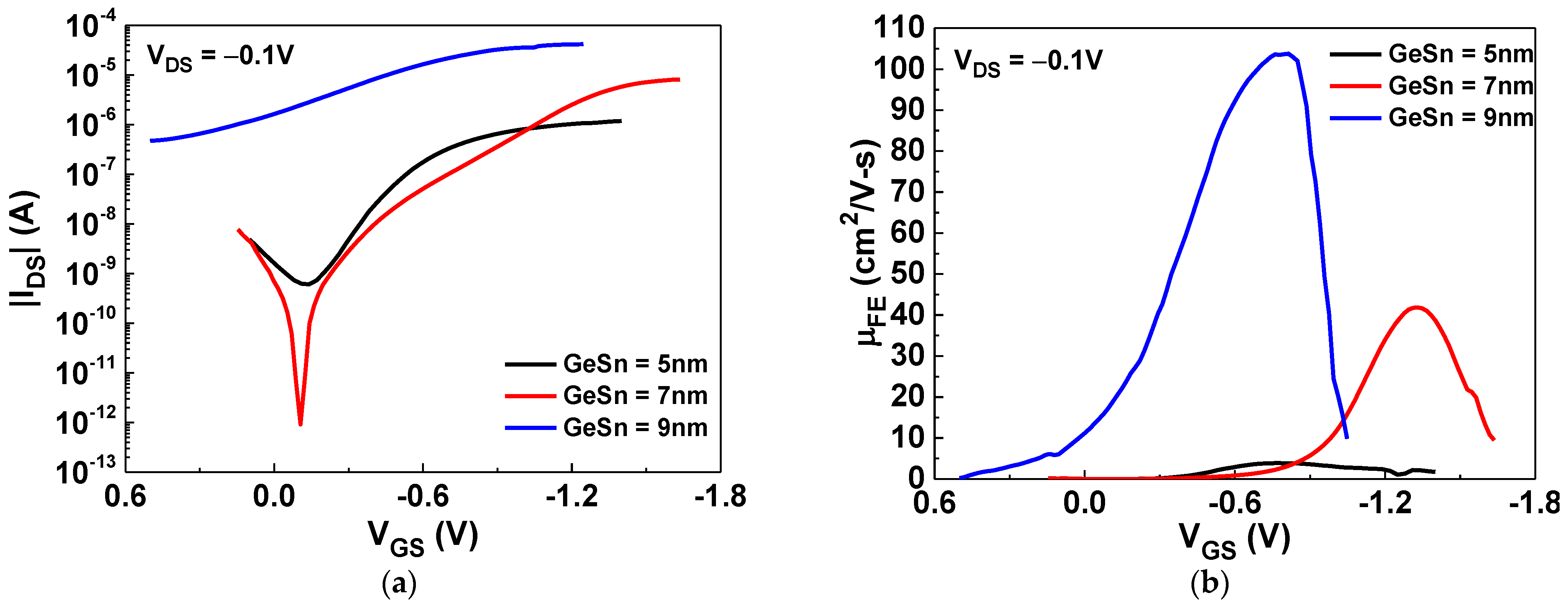
Figure 1a shows the drain-source current versus the gate-source voltage (IDS-VGS) characteristics of GeSn/SiO2/HfO2 pTFTs with GeSn thicknesses of 5, 7, or 9 nm. The device with a channel thickness of 7 nm exhibited the best performance, with an ION/IOFF value of 8.9 × 10⁶. The gate-source current versus the gate-source voltage (|IGS|−VGS) of the TFT devices with different GeSn film thicknesses is displayed in Figure S2. Figure 1b displays the field-effect mobility versus the gate-source voltage (μFE-VGS) characteristics of the GeSn pTFTs, which were measured under a small VDS (−0.1 V). Here, the hole mobility values increase with the GeSn layer thickness, which is consistent with the increasing trend of ION. This is due to the decreased depletion width of GeSn by the gate and surface potential, which provides more carriers to transport from the source to the drain. The peak mobilities of the GeSn TFTs with GeSn thicknesses of 5, 7, and 9 nm were 3.9, 41.8, and 103.8 cm2/V·s, respectively. Although the device with a GeSn thickness of 9 nm showed the highest mobility, the poor SS (1560 mV/dec) and an ION/IOFF of only 75 make it unsuitable for device applications. The thin (5 nm) channel thickness exhibited 10 times lower mobility than the 7 nm GeSn device, which is attributed to the lack of carriers and strong interfacial scattering [26,27]. The 7 nm GeSn TFT device showed a large ION/IOFF, of 8.9 × 10⁶; a good SS value, of 311 mV/dec; and a high μFE, of 41.8 cm2/V·s, which is much better than those of traditional oxide pTFTs and shows the high potential for future SoP and monolithic brain-mimicking IC applications. In addition, such a high hole mobility is similar to that of the single-crystal Si used for standard ICs [42]. It is important to note that the nanosheet GeSn thickness of 7 nm is exactly the same as that of the single-crystal Si nanosheet FET used for 2 nm node technology manufacture.
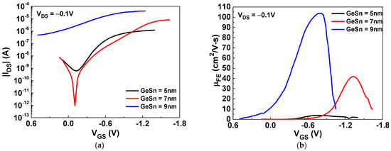
Figure 1.
The (a) |IDS|–VGS and (b) μFE–VGS characteristics of the GeSn/SiO2/HfO2 pTFTs with different channel thicknesses.
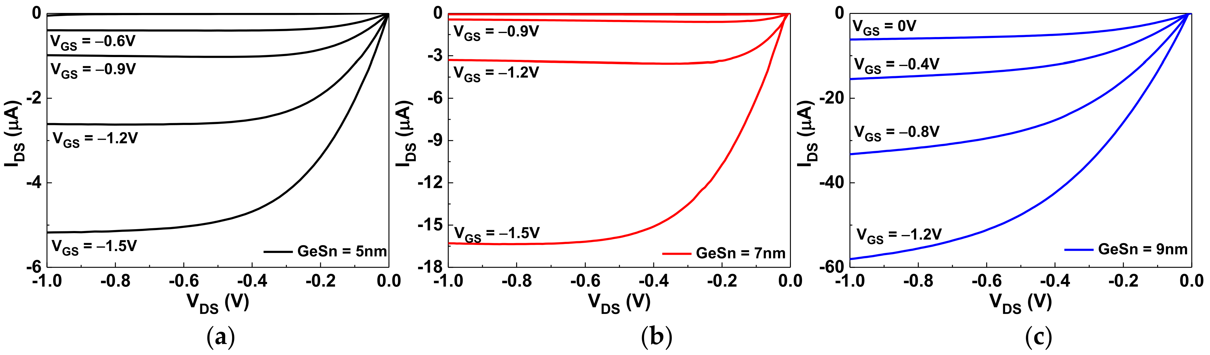
The drain-source current versus the drain-source voltage (IDS-VDS) characteristics of GeSn pTFT devices with GeSn thicknesses of 5, 7, or 9 nm are shown in Figure 2a–c, respectively. The saturation IDS increases with increasing GeSn channel thickness, and a higher IDS leads to a higher μFE, as shown in Figure 1b. The IDS–VDS curves for 5 and 7 nm thicknesses of GeSn display good IDS saturation characteristics. In contrast, the 9 nm thick GeSn device shows poor saturation characteristics, which is due to excessive carrier conduction and poor channel pinch-off. In addition, the non-negligible IDS at VGS = 0 V will lead to high standby power.
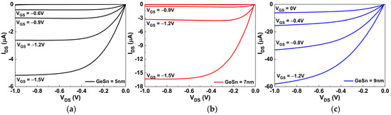
Figure 2.
The IDS–VDS characteristics of the GeSn/SiO2/HfO2 pTFTs with (a) 5 nm, (b) 7 nm, and (c) 9 nm channel thicknesses.
Figure 3a illustrates the schematic device structure diagram of the bottom-gate GeSn pTFT. High-work-function Ni was formed on GeSn and used as the drain and source electrodes. The HfO2 and thin SiO2 stack served as the gate dielectric, in which SiO2 was used to minimize the remote phonon scattering effects from high-κ HfO2 [17,20,43,44,45]. In this study, a high-κ gate dielectric was used to increase the gate capacitance and ION, which is widely used for Si metal-oxide-semiconductor (MOS) FET and TFT devices. The device structure was further verified using cross-sectional TEM. As depicted in Figure 3b, the thicknesses of the GeSn channel layer and the SiO2 interfacial layer on high-k HfO2 are 7 and 2 nm, respectively. Here, the crystal grains in the TEM image are marked with a yellow dashed line. Figure S3a and Figure S3b show the TEM images of the device with GeSn layers annealed at 300 and 350 °C, respectively. A 2 nm SiO2 layer is added between HfO2 and GeSn. Via an atomic force microscope (AFM), Figure S4 exhibits the surface roughness of the GeSn layer annealed at different temperatures. The surface roughness of the GeSn layer degrades with increasing annealing temperature. The device annealed at 300 °C displays the best surface smoothness and uniformity (Figure S4a); however, the hole μFE is only 3.71 cm2/V·s, as depicted in Figure S5. The crystalline size depends on the GeSn thickness and annealing temperature. However, the increasing GeSn thickness increases the device IOFF leakage. The increasing annealing temperature degrades mobility by increasing surface roughness (Figure S4c). Therefore, there is a tradeoff between the channel layer surface roughness, uniformity, and carrier mobility. The 350 °C annealing is the best condition to increase μFE of the nanosheet FET. Further hole μFE and IOFF tradeoff may be possible by using a 6 nm GeSn layer.
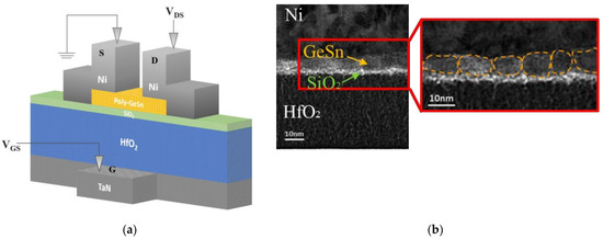
Figure 3.
(a) The schematic device diagram and (b) the cross-sectional TEM image of a bottom-gate GeSn pTFT.
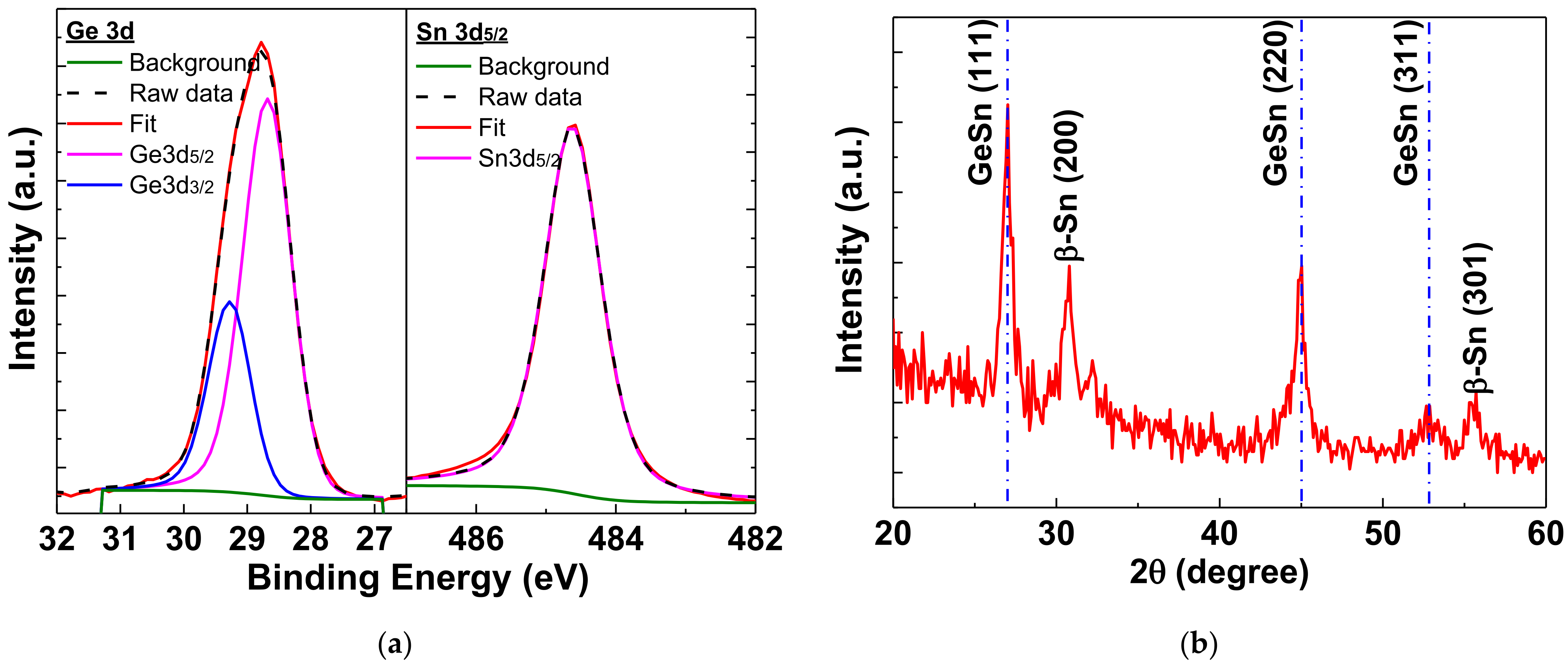
XPS analysis was conducted to examine the composition of the GeSn layer. Through XPS measurements, as depicted in Figure S6, the ratio of Ge/Sn was determined to be 7. Figure 4a shows the Ge 3d and Sn 3d5/2 core spectra. There is no oxide compound signal of GeOx or SnOx in the Ge 3d and Sn3d5/2 spectra [46], which is one of the reasons for the high mobility. As depicted in Figure 4b, the XRD analysis reveals that the GeSn layer is polycrystalline after annealing at 350 °C. The diffraction peaks related to GeSn are crystal orientations GeSn (111), GeSn (220), and GeSn (311), corresponding to 2θ values of 27.0°, 45.0°, and 52.7°, respectively, which are similar to previously published data [29,47,48,49]. Additionally, at 2θ = 30.79° and 55.03°, diffraction peaks of β-Sn (200) and β-Sn (301) were observed [22,49,50], which could be the Sn precipitated during the rapid thermal annealing at 350 °C.
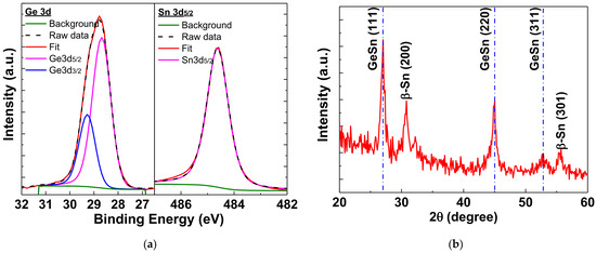
Figure 4.
The (a) XPS spectra of Ge 3d and Sn 3d5/2 and (b) XRD analyses of GeSn film annealed at 350 °C.
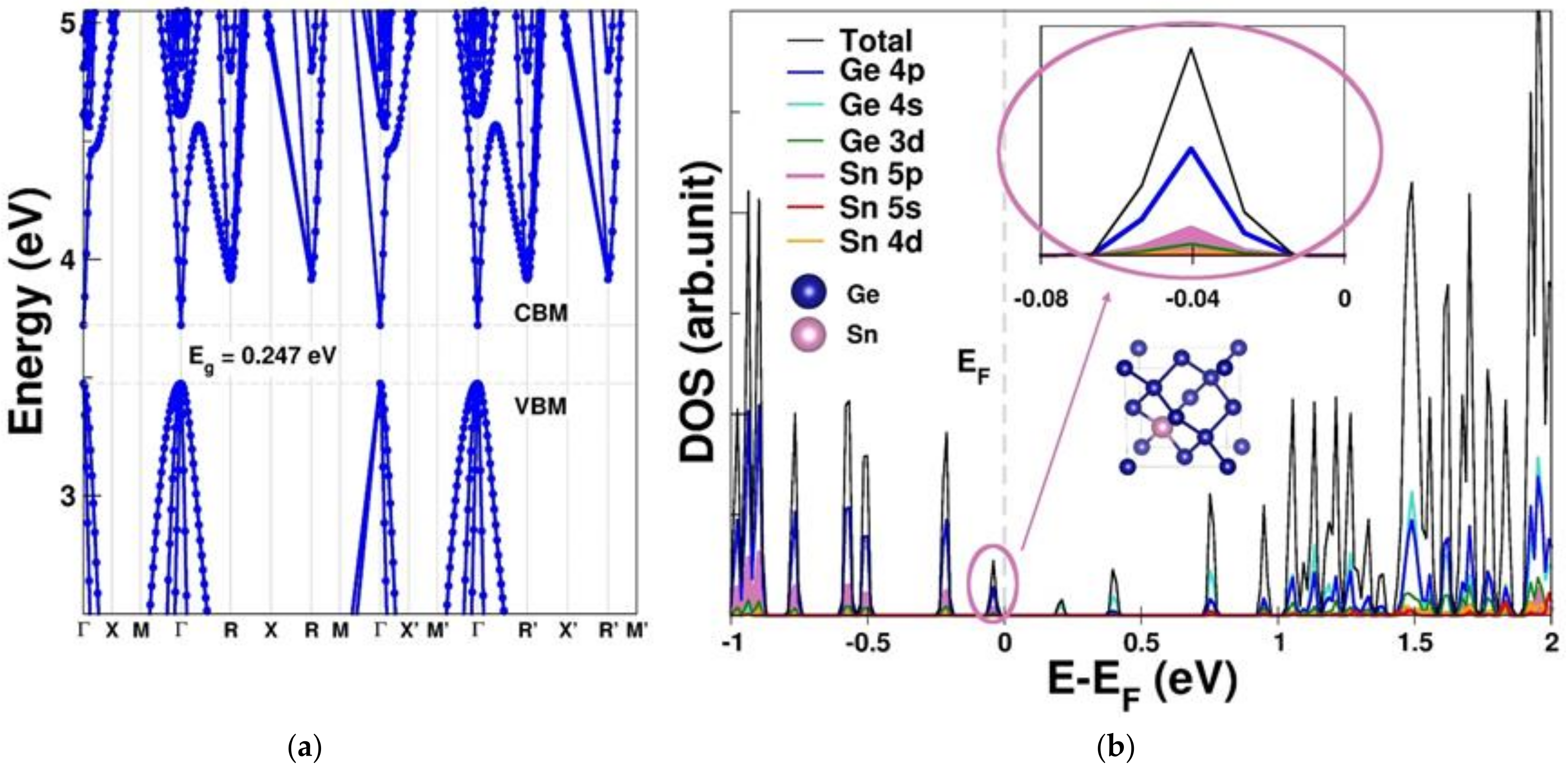
To thoroughly comprehend the fundamental physical properties related to the hole mobility of the GeSn pTFT, the electronic structure and hole effective mass were computed based on first principles. Figure 5a,b present the band structure and density of states (DOS) of Ge0.875Sn0.125, respectively, revealing a direct bandgap of 0.25 eV. Our calculated outcome is analogous to that of previous work, where the bandgap of GeSn is expected to turn directly when the Sn/Ge ratio is larger than 8% [33]. The contributions of each orbital in the valence band maximum (VBM) of were further investigated using the total DOS, the orbital-decomposed DOS, the projected DOS of Sn, and the local DOS near the VBM, as shown in Figure 5b. These results lead to the following conclusions: (1) Both the valence band and the conduction band are primarily contributed by the Ge orbitals (Figure S7). (2) Figure 5b shows that the topmost valence band is predominantly contributed by both Ge 4p and Sn 5p orbitals, reinforcing the electron density in the vicinity of the VBM. (3) In contrast, for the region near and beyond the conduction band minimum (CBM), the major contribution is from all Ge orbitals (4s > 4p > 3d), but not the Sn orbitals, supporting the predominant contribution of Sn orbitals to the VBM. In addition, the calculated effective mass and the energy bandgap of Ge0.875Sn0.125 from Figure 5a are summarized in Table 1. The heavy-hole effective mass at the point () is −0.225 (the unit of free electron mass), while the light-hole effective mass at the point () is −0.028 , indicating that the heavy-hole effective mass dominates the total transport mass. Table 1 also shows that the of Ge0.875Sn0.125 is less than that (0.28 m0) of Ge and half that of Si (0.49 m0) [51]. This is the reason why GeSn has been proposed for pMOS or pTFT. However, the reported GeSn pTFTs in the literature suffered from poor ION/IOFF [26,27,28,29], which is due to the leakage current of the small energy bandgap.

Figure 5.
(a) The band structure and (b) the total density of states (DOS), the orbital-decomposed DOS, the projected DOS of Sn, and the local DOS near the VBM (insert) of Ge0.875Sn0.125.

Table 1.
Comparison of effective masses at gamma of heavy-hole () and light-hole () direct and indirect bandgaps ( and ) of Ge0.875Sn0.125, Ge [51], and Si [51].
Table 2 displays the crucial TFT device parameters of various poly-GeSn TFTs [26,27,28,29]. The remarkably high ION/IOFF and relatively sharp SS are the advantages of this study. The excellent device performance is due to the ultra-thin nanosheet GeSn layer, with a thickness of only 7 nm. Although the mobility can reach higher than 100 cm2/V·s with a thickness of 9 nm, the SS and ION/IOFF values are degraded and unfavorable for transistor applications. The low process temperature (350 °C) and high-performance nanosheet GeSn pTFT in this work are promising for SoP and monolithic 3D IC applications.
Table 2.
Comparison of several important parameters among various poly-GeSn TFT devices.
4. Conclusions
In this study, a high-performance poly-GeSn pTFT was achieved with an excellent transistor performance (41.8 cm2/V·s), a sharp SS (0.31 V/dec), and a large ION/IOFF value (8.9 × 10⁶). This was achieved using an ultra-thin (7 nm) nanosheet GeSn layer that can be depleted by gate and surface potentials. The high hole mobility is related to its small heavy-hole effective mass, of 0.225m0. The remarkably high performance and low thermal budget of the nanosheet GeSn pTFT are an enabling technology for CTFTs, SoP, monolithic 3D ICs, and 3D brain-mimicking ICs.
Supplementary Materials
The following are available online at https://www.mdpi.com/article/10.3390/nano12020261/s1, Figure S1: Optimized structure of the diamond cubic model with the lattice constant of 5.763 Å, containing eight atoms by first-principles calculations, Figure S2: The |IGS|−VGS characteristics of the GeSn/SiO2/HfO2 pTFTs with different channel thickness, Figure S3: The cross-sectional TEM image of GeSn pTFT with GeSn annealed at (a) 300 and (b) 350 °C, Figure S4: The surface roughness of GeSn films annealed at (a) 300 °C, (b) 350 °C and (c) 400 °C measured by AFM, Figure S5: The |IDS|−VGS and μFE−VGS characteristics of the GeSn pTFTs with 7 nm channel thickness and annealed at 300 °C, Figure S6: The XPS spectrum of , Figure S7: Total density of state (DOS) and projected DOS of Ge and Sn of by first-principles calculations.
Author Contributions
T.J.Y. did the experiments; A.C. is the principal investigator (PI) to monitor the project; W.K.C. and H.-Y.T.C. did the simulation; V.G. is the co-PI for this work. All authors have read and agreed to the published version of the manuscript.
Funding
This research was funded by the Ministry of Science and Technology of Taiwan, project no. 110-2221-E-A49-137-MY3 and 108-2112-M-007-023-MY3. The computing resource were supported by TAIWANIA in the National Center for High-Performance Computing (NCHC) in Taiwan.
Institutional Review Board Statement
Not applicable.
Informed Consent Statement
Not applicable.
Data Availability Statement
The data presented in this study are available on request from the corresponding author. The data are not publicly available due to privacy.
Acknowledgments
We would like to thank the National Yang Ming Chiao Tung University Nano Facility Center and the Taiwan Semiconductor Research Institute for providing the laboratory instruments. We would also like to thank C. C. Huang for assisting in the device fabrication during his master’s degree study.
Conflicts of Interest
The authors declare no conflict of interest.
References
- Kwon, J.Y.; Son, K.S.; Jung, J.S.; Kim, T.S.; Ryu, A.K.; Park, K.B.; Yoo, B.W.; Kim, J.W.; Lee, Y.G.; Park, K.C.; et al. Bottom-gate Gallium Indium Zinc Oxide thin-film transistor array for high-resolution AMOLED display. IEEE Electron. Device Lett. 2008, 29, 1309–1311. [Google Scholar] [CrossRef]
- Petti, L.; Munzenrieder, N.; Vogt, C.; Faber, H.; Buthe, L.; Cantarella, G.; Bottacchi, F.; Anthopoulos, T.D.; Troster, G. Metal oxide semiconductor thin-film transistors for flexible electronics. Appl. Phys. Rev. 2016, 3, 021303. [Google Scholar] [CrossRef] [Green Version]
- Fortunato, E.; Barquinha, P.; Martins, R. Oxide semiconductor thin-film transistors: A review of recent advances. Adv. Mater. 2012, 24, 2945–2986. [Google Scholar] [CrossRef] [PubMed]
- Nomura, K.; Ohta, H.; Takagi, A.; Kamiya, T.; Hirano, M.; Hosono, H. Room-temperature fabrication of transparent flexible thin-film transistors using amorphous oxide semiconductors. Nature 2004, 432, 488–492. [Google Scholar] [CrossRef] [PubMed]
- Yin, X.; Deng, S.; Li, G.; Zhong, W.; Chen, R.; Li, G.; Yeung, F.S.Y.; Wong, M.; Kwok, H.S. Low leakage current vertical thin-film transistors with InSnO-stabilized ZnO Channel. IEEE Electron. Device Lett. 2019, 41, 248–257. [Google Scholar] [CrossRef]
- Su, N.C.; Wang, S.J.; Huang, C.C.; Chen, Y.H.; Huang, H.Y.; Chiang, C.K.; Chin, A. Low-voltage-driven flexible InGaZnO thin-film transistor with small subthreshold swing. IEEE Electron. Device Lett. 2010, 31, 680–682. [Google Scholar]
- Nomura, K.; Kamiya, T.; Hosono, H. Ambipolar oxide thin-film transistor. Adv. Mater. 2011, 23, 3431–3434. [Google Scholar] [CrossRef]
- Chin, A.; Yen, T.J.; Shih, C.W.; Chen, Y.D. High mobility metal-oxide devices for display SoP and 3D brain-mimicking IC. Proc. Int. Disp. Workshops 2019, 26, 455–457. [Google Scholar] [CrossRef]
- Chin, A.; Chen, Y.D. Technologies toward three-dimensional brain-mimicking IC architecture. In Proceedings of the 2019 Electron Devices Technology and Manufacturing Conference (EDTM), Singapore, 12–15 March 2019; pp. 472–474. [Google Scholar]
- Chin, A.; Yen, T.J.; Chen, Y.D.; Shih, C.W.; Gritsenko, V. High Mobility Oxide Complementary TFTs for System-on-Display and Three-Dimensional Brain-Mimicking IC. In Proceedings of the International Conference on Display Technology, Wuhan, China, 11–13 October 2020; pp. 292–294. [Google Scholar]
- Felfel, A.M.; Datta, K.; Dutt, A.; Veluri, H.; Zaky, A.; Thean, A.V.Y.; Aly, M.M.S. Quantifying the benefits of monolithic 3D computing systems enabled by TFT and RRAM. In Proceedings of the 2020 Design, Automation & Test in Europe Conference & Exhibition (DATE), Grenoble, France, 9–13 March 2020; pp. 43–48. [Google Scholar]
- Kwon, J.; Takeda, Y.; Shiwaku, R.; Tokito, S.; Cho, K.; Jung, S. Three-dimensional monolithic integration in flexible printed organic transistors. Nat. Commun. 2019, 10, 54. [Google Scholar] [CrossRef] [Green Version]
- Liang, L.Y.; Cao, H.T.; Chen, X.B.; Liu, Z.M.; Zhuge, F.; Luo, H.; Li, J.; Lu, Y.C.; Lu, W. Ambipolar inverters using SnO thin-film transistors with balanced electron and hole mobilities. Appl. Phys. Lett. 2012, 100, 263502. [Google Scholar] [CrossRef]
- Ohshima, H.; Morozumi, S. Future trends for TFT integrated circuits on glass substrates. In Proceedings of the International Electron Devices Meeting (IEDM) Technical Digest, Washington, DC, USA, 7–9 December 1989; pp. 157–160. [Google Scholar]
- Zhong, C.W.; Lin, H.C.; Liu, K.C.; Huang, T.Y. Improving electrical performances of p-type SnO thin-film transistors using double-gated structure. IEEE Electron Device Lett. 2015, 36, 1053–1055. [Google Scholar] [CrossRef]
- Shih, C.W.; Chin, A.; Lu, C.F.; Yi, S.H. Extremely high mobility ultra-thin metal-oxide with ns2np2 configuration. In Proceedings of the International Electron Devices Meeting (IEDM) Technical Digest, Washington, DC, USA, 7–9 December 2015; pp. 145–148. [Google Scholar]
- Yen, T.J.; Chin, A.; Gritsenko, V. High performance top-gate thin film transistor with an ultra-thin channel layer. Nanomaterials 2020, 10, 2145. [Google Scholar] [CrossRef]
- Shih, C.W.; Chin, A.; Lu, C.F.; Su, W.F. Remarkably high mobility ultra-thin-film metal-oxide transistor with strongly overlapped orbitals. Sci. Rep. 2016, 6, 19023. [Google Scholar] [CrossRef] [Green Version]
- Shih, C.W.; Yen, T.J.; Chin, A.; Lu, C.F.; Su, W.F. Low-temperature processed tin oxide transistor with ultraviolet irradiation. IEEE Electron Device Lett. 2019, 40, 909–912. [Google Scholar] [CrossRef]
- Shih, C.W.; Chin, A. New material transistor with record-high field-effect mobility among wide-band-gap semiconductors. ACS Appl. Mater. Interfaces 2016, 8, 19187–19191. [Google Scholar] [CrossRef] [Green Version]
- Shih, C.W.; Chin, A. Remarkably High mobility thin-film transistor on flexible substrate by novel passivation material. Sci. Rep. 2017, 7, 1147. [Google Scholar] [CrossRef] [PubMed] [Green Version]
- Shih, C.W.; Chin, A.; Lu, C.F.; Su, W.F. Remarkably high hole mobility metal-oxide thin-film transistors. Sci. Rep. 2018, 8, 889. [Google Scholar] [CrossRef] [Green Version]
- Yen, T.J.; Chin, A.; Gritsenko, V. Exceedingly high performance top-gate p-type SnO thin film transistor with a nanometer scale channel layer. Nanomaterials 2021, 11, 92. [Google Scholar] [CrossRef] [PubMed]
- Pattanasattayavong, P.; Thomas, S.; Adamopoulos, G.; McLachlan, M.A.; Anthopoulos, T.D. P-channel thin-film transistors based on spray-coated Cu2O films. Appl. Phys. Lett. 2013, 102, 163505. [Google Scholar] [CrossRef] [Green Version]
- Lin, T.; Li, X.; Jang, J. High performance p-type NiOX thin-film transistor by Sn doping. Appl. Phys. Lett. 2016, 108, 233503. [Google Scholar] [CrossRef]
- Zhang, L.; Hong, H.; Yu, C.; Li, C.; Chen, S.; Huang, W.; Wang, J.; Wang, H. Poly-GeSn junctionless thin-film transistors on insulators fabricated at low temperatures via pulsed laser annealing. Phys. Status Solidi RRL 2019, 13, 1900420. [Google Scholar] [CrossRef]
- Galluccio, E.; Dohert, J.; Biswas, S.; Holmes, J.D.; Duffy, R. Field-effect transistor figures of merit for vapor–liquid–solid-grown Ge1−xSnx (x = 0.03–0.09) nanowire devices. ACS Appl. Electron. Mater. 2020, 2, 1226–1234. [Google Scholar] [CrossRef]
- Chou, C.P.; Lin, Y.X.; Wu, Y.H. Implementing p-Channel junctionless thin-film transistor on poly-Ge0.95Sn0.05 film formed by amorphous GeSn deposition and annealing. IEEE Electron Device Lett. 2018, 39, 1187–1190. [Google Scholar]
- Miyazaki, R.; Hara, A. Four-terminal polycrystalline Ge1−xSnx thin film transistors using copper-induced crystallization on glass substrates and their application to enhancement/depletion inverters. Jpn. J. Appl. Phys. 2020, 59, 051008. [Google Scholar] [CrossRef]
- Nakano, Y.; Saeki, S.; Morikawa, T. Optical bandgap widening of p-type Cu2O films by nitrogen doping. Appl. Phys. Lett. 2009, 94, 022111. [Google Scholar] [CrossRef] [Green Version]
- Hautier, G.; Miglio, A.; Ceder, G.; Rignanese, G.-M.; Gonze, X. Identification and design principles of low hole effective mass p-type transparent conducting oxides. Nat. Commun. 2013, 4, 2292. [Google Scholar] [CrossRef] [Green Version]
- Lei, D.; Wang, W.; Zhang, Z.; Pan, J.; Gong, X.; Liang, G.; Tok, E.S.; Yeo, Y.C. Ge0.83Sn0.17 p-channel metal-oxide-semiconductor field-effect transistors: Impact of sulfur passivation on gate stack quality. J. Appl. Phys. 2016, 119, 024502. [Google Scholar] [CrossRef] [Green Version]
- Gupta, S.; Chen, R.; Magyari-Kope, B.; Lin, H.; Yang, B.; Nainani, A.; Nishi, Y.; Harris, J.S.; Saraswat, K.C. GeSn technology: Extending the Ge electronics roadmap. In Proceedings of the International Electron Devices Meeting (IEDM) Technical Digest, Washington, DC, USA, 5–7 December 2011; pp. 398–401. [Google Scholar]
- Sau, J.D.; Cohen, M.L. Possibility of increased mobility in Ge-Sn alloy system. Phys. Rev. B 2007, 75, 045208. [Google Scholar] [CrossRef]
- Kresse, G.; Furthmüller, J. Efficiency of ab-initio total energy calculations for metals and semiconductors using a plane-wave basis set. Comput. Mater. Sci. 1996, 6, 15–50. [Google Scholar] [CrossRef]
- Blöchl, P.E. Projector augmented-wave method. Phys. Rev. B 1994, 50, 17953–17979. [Google Scholar] [CrossRef] [Green Version]
- Kresse, G.; Joubert, J. From ultrasoft pseudopotentials to the projector augmented-wave method. Phys. Rev. B 1999, 59, 1758–1775. [Google Scholar] [CrossRef]
- Krukau, A.V.; Vydrov, O.A.; Izmaylov, A.F.; Scuseria, G.E. Influence of the exchange screening parameter on the performance of screened hybrid functionals. J. Chem. Phys. 2006, 125, 224106. [Google Scholar] [CrossRef] [PubMed]
- Hinuma, Y.; Pizzi, G.; Kumagai, Y.; Oba, F.; Tanaka, I. Band structure diagram paths based on crystallography. Comput. Mater. Sci. 2017, 128, 140–184. [Google Scholar] [CrossRef] [Green Version]
- Togo, A.; Tanaka, I. Spglib: A software library for crystal symmetry search. arXiv 2018, arXiv:1808.01590. [Google Scholar]
- Wang, V.; Xu, N.; Liu, J.C.; Tang, G.; Geng, W.T. VASPKIT: A user-friendly interface facilitating high-throughput computing and analysis using vasp code. Comput. Phys. Commun. 2021, 267, 108033. [Google Scholar] [CrossRef]
- Sun, G.; Sun, Y.; Nishida, T.; Thompson, E.S. Hole mobility in silicon inversion layers: Stress and surface orientation. J. Appl. Phys. 2007, 102, 084501. [Google Scholar] [CrossRef]
- Yu, D.S.; Chin, A.; Laio, C.C.; Lee, C.F.; Cheng, C.F.; Chen, W.J.; Zhu, C.; Li, M.-F.; Yoo, W.J.; McAlister, S.P.; et al. 3D GOI CMOSFETs with novel IrO2(Hf) dual gates and high-κ dielectric on 1P6M-0.18 μm-CMOS. In Proceedings of the International Electron Devices Meeting (IEDM) Technical Digest, San Francisco, CA, USA, 13–15 December 2004; pp. 181–184. [Google Scholar]
- Cheng, C.F.; Wu, C.H.; Su, N.C.; Wang, S.J.; McAlister, S.P.; Chin, A. Very low Vt [Ir-Hf]/HfLaO CMOS using novel self-aligned low temperature shallow junctions. In Proceedings of the International Electron Devices Meeting (IEDM) Technical Digest, Washington, DC, USA, 10–12 December 2007; pp. 333–336. [Google Scholar]
- Yu, X.; Zhu, C.; Yu, M.; Li, M.F.; Chin, A.; Tung, C.H.; Gui, D.; Kwong, D.L. Advanced MOSFETs using HfTaON/SiO2 gate dielectric and TaN metal gate with excellent performances for low standby power application. In Proceedings of the International Electron Devices Meeting (IEDM) Technical Digest, Washington, DC, USA, 5 December 2005. [Google Scholar] [CrossRef]
- Wang, W.; Lei, D.; Dong, Y.; Gong, X.; Tok, E.S.; Yeo, Y.C. Digital etch technique for forming ultra-scaled germanium-tin (Ge1−xSnx) fin structure. Sci. Rep. 2017, 7, 1835. [Google Scholar] [CrossRef] [Green Version]
- Kim, M.; Fan, W.J.; Seo, J.H.; Cho, N.; Liu, S.C.; Geng, D.; Liu, Y.H.; Gong, S.Q.; Wang, X.D.; Zhou, W.D.; et al. Polycrystalline GeSn thin films on Si formed by alloy evaporation. Appl. Phys. Express 2015, 8, 061301. [Google Scholar] [CrossRef]
- Li, H.; Brouillet, J.; Salas, A.; Wang, X.; Liu, J. Low temperature growth of high crystallinity GeSn on amorphous layers for advanced optoelectronics. Opt. Mater. Express 2013, 3, 1385–1396. [Google Scholar] [CrossRef]
- Cho, Y.J.; Kim, C.H.; Im, H.S.; Myung, Y.; Kim, H.S.; Back, S.H.; Lim, Y.R.; Jung, C.S.; Jang, D.M.; Park, J.; et al. Germanium−Tin alloy nanocrystals for high-performance lithium ion batteries. Phys. Chem. Chem. Phys. 2013, 15, 11691–11695. [Google Scholar] [CrossRef]
- Mittal, J.; Lin, K.L. Crystal structure variations of Sn nanoparticles upon heating. J. Electron. Mater. 2018, 47, 2394–2401. [Google Scholar] [CrossRef]
- Van Zeghbroeck, B. Principles of Semiconductor Devices; Colarado University: Boulder, CO, USA, 2004; p. 34. [Google Scholar]

Publisher’s Note: MDPI stays neutral with regard to jurisdictional claims in published maps and institutional affiliations. |
© 2022 by the authors. Licensee MDPI, Basel, Switzerland. This article is an open access article distributed under the terms and conditions of the Creative Commons Attribution (CC BY) license (https://creativecommons.org/licenses/by/4.0/).