
STEM Tools for Semiconductor Characterization: Beyond High-Resolution Imaging


Abstract
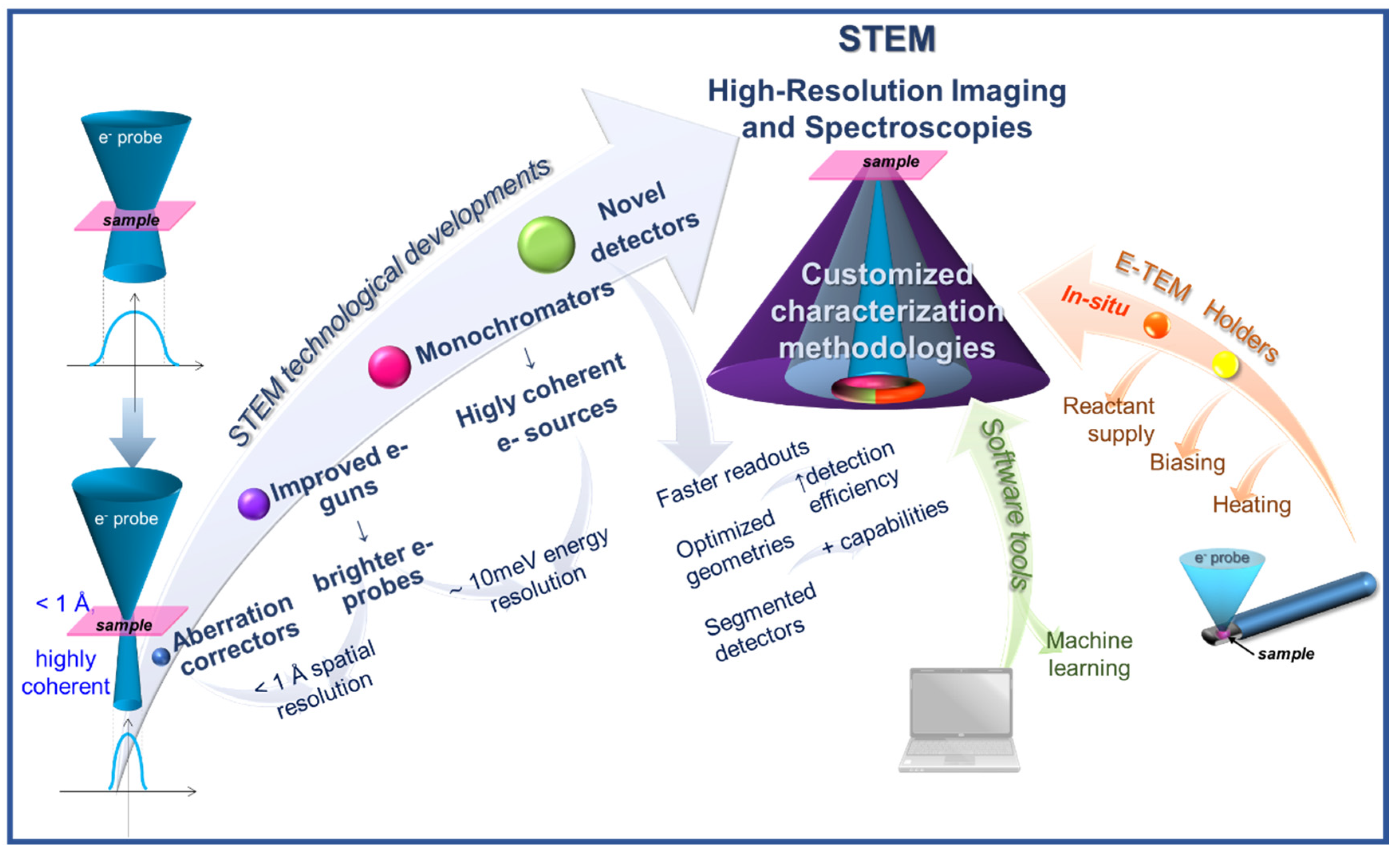
:1. Why Choose STEM
2. STEM Imaging Techniques
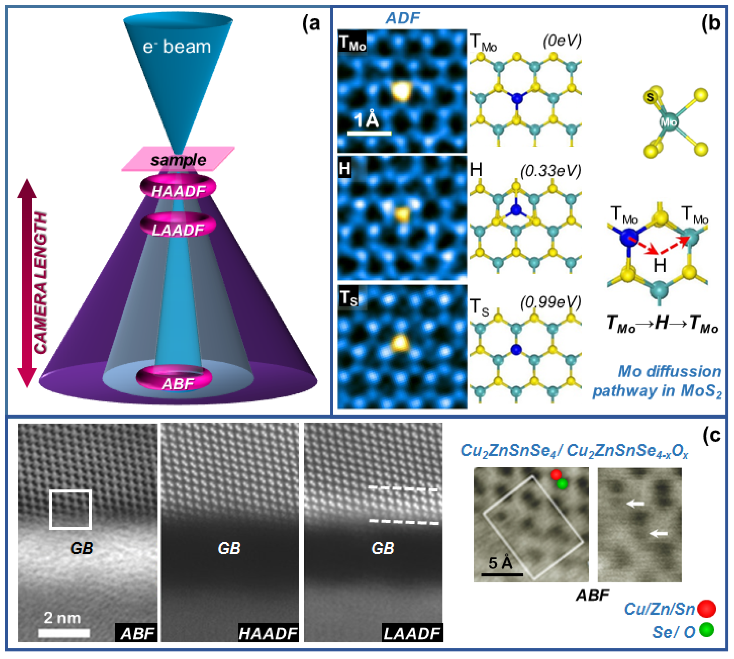
2.1. Annular Detectors
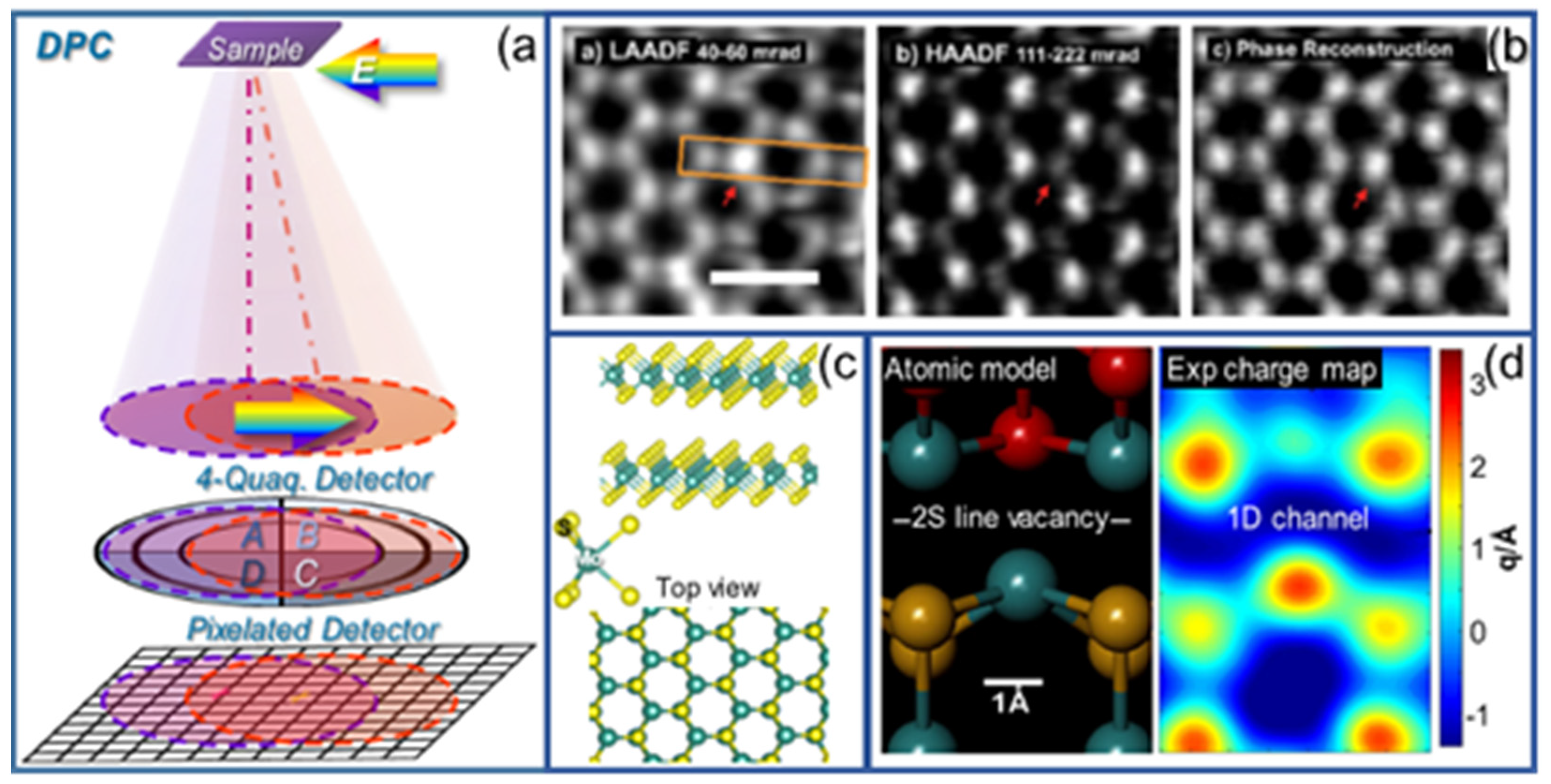
2.2. Segmented Detectors: 4D-STEM
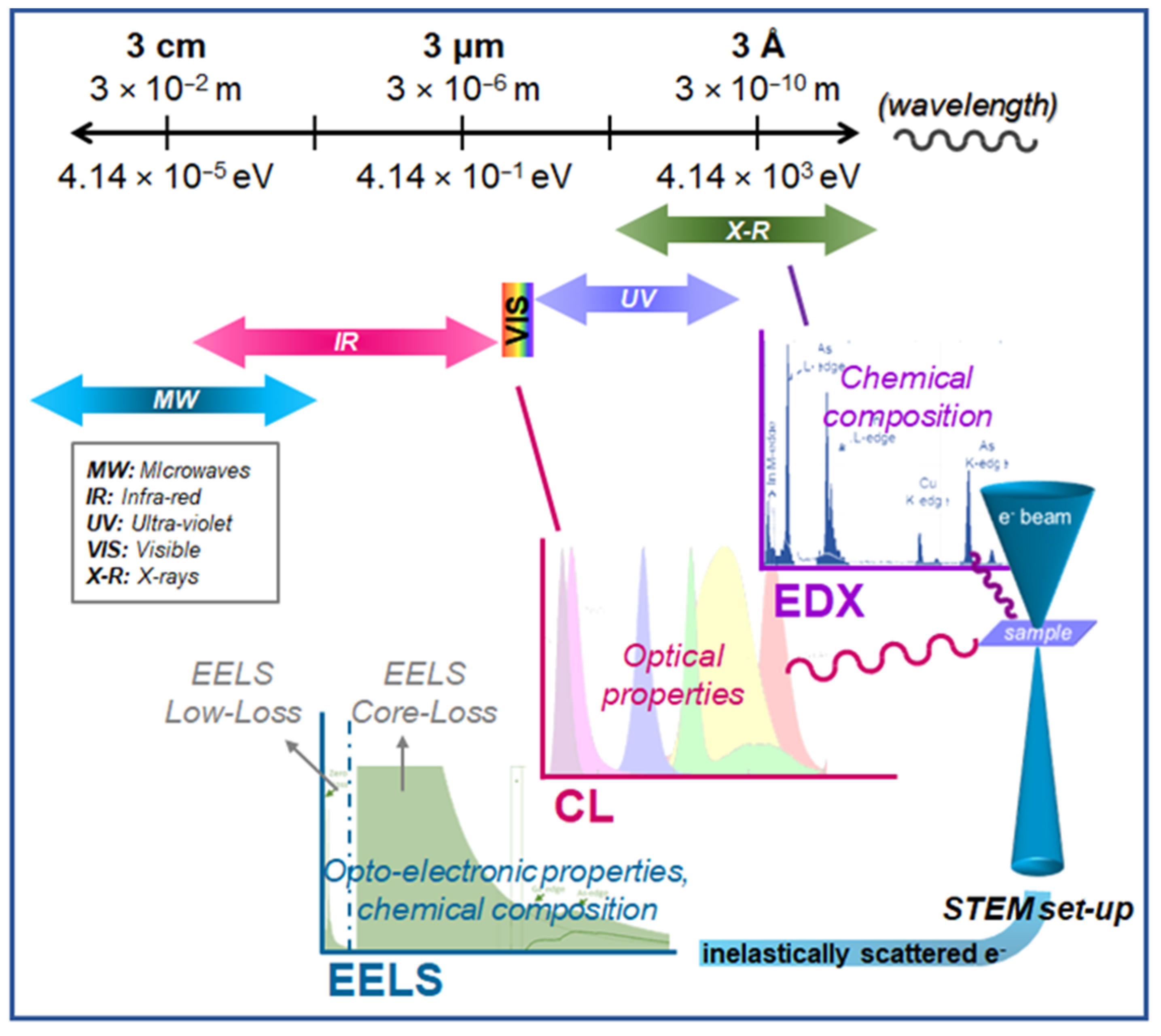
3. Spectroscopy in STEM
3.1. Electron Energy-Loss Spectroscopy (EELS)
3.1.1. Core-Loss EELS
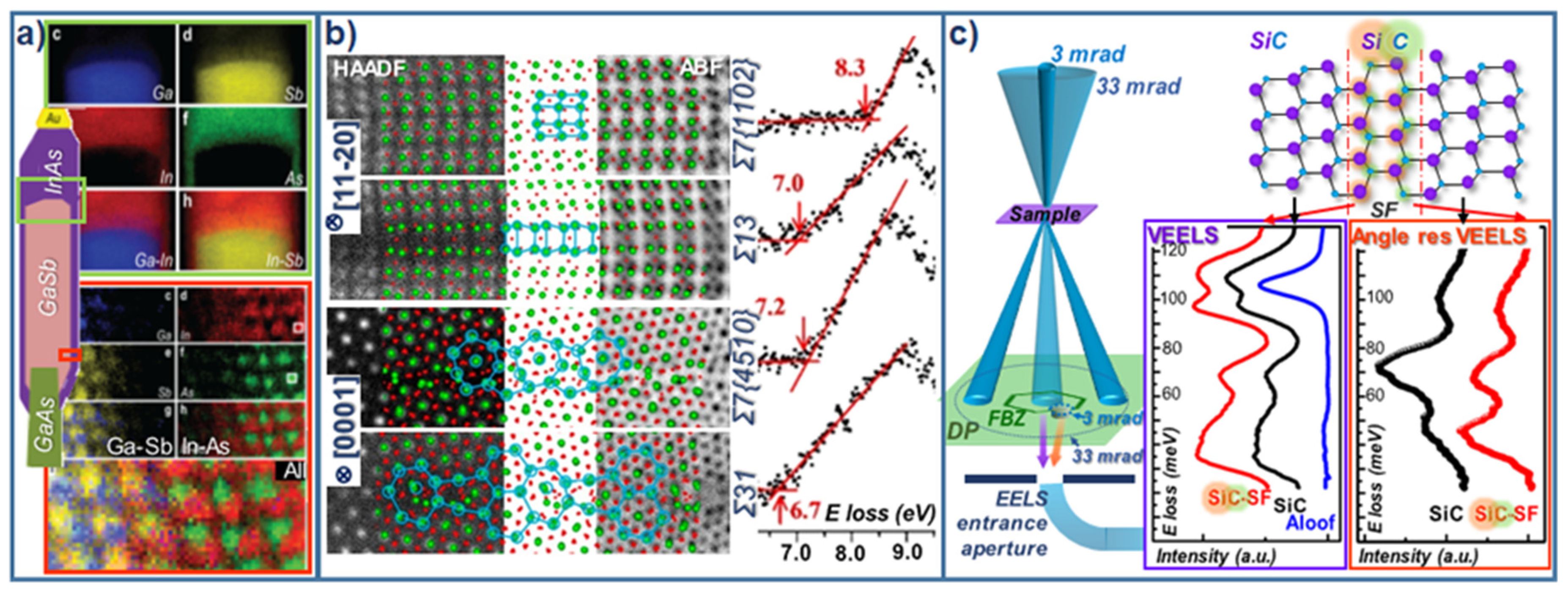
3.1.2. Low-Loss EELS
3.2. Further STEM Spectroscopies
3.2.1. Energy Dispersive X-ray Spectroscopy
3.2.2. Cathodoluminiscence
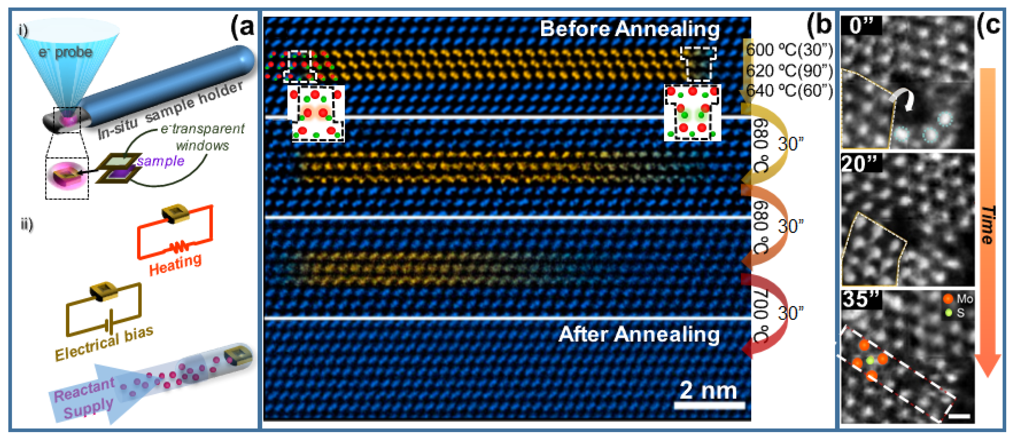
4. In Situ STEM
5. Machine Learning and STEM
6. Overview and Outlook
Author Contributions
Funding
Institutional Review Board Statement
Informed Consent Statement
Acknowledgments
Conflicts of Interest
References
- Humphreys, C.J. Fundamental concepts of STEM imaging. Ultramicroscopy 1981, 7, 7–12. [Google Scholar] [CrossRef]
- Ciston, J.; Johnson, I.J.; Draney, B.R.; Ercius, P.; Fong, E.; Goldschmidt, A.; Joseph, J.M.; Lee, J.R.; Mueller, A.; Ophus, C.; et al. The 4D Camera: Very High Speed Electron Counting for 4D-STEM. Microsc. Microanal. 2019, 25, 1930–1931. [Google Scholar] [CrossRef] [Green Version]
- Zamani, R.R.; Arbiol, J. Understanding semiconductor nanostructures via advanced electron microscopy and spectroscopy. Nanotechnology 2019, 30, 262001. [Google Scholar] [CrossRef]
- Nellist, P.D.; Chisholm, M.F.; Dellby, N.; Krivanek, O.L.; Murfitt, M.F.; Szilagyi, Z.S.; Lupini, A.R.; Borisevich, A.; Sides, W.H.; Pennycook, S.J. Direct Sub-Angstrom Imaging of a Crystal Lattice. Science 2004, 305, 1741. [Google Scholar] [CrossRef] [PubMed]
- Crewe, A.V.; Wall, J.; Langmore, J. Visibility of Single Atoms. Science 1970, 168, 1338–1340. [Google Scholar] [CrossRef] [PubMed]
- Hong, J.; Pan, Y.; Hu, Z.; Lv, D.; Jin, C.; Ji, W.; Yuan, J.; Zhang, Z. Direct Imaging of Kinetic Pathways of Atomic Diffusion in Monolayer Molybdenum Disulfide. Nano Lett. 2017, 17, 3383–3390. [Google Scholar] [CrossRef] [PubMed] [Green Version]
- Kim, J.H.; Choi, S.Y.; Choi, M.; Gershon, T.; Lee, Y.S.; Wang, W.; Shin, B.; Chung, S.Y. Atomic-Scale Observation of Oxygen Substitution and Its Correlation with Hole-Transport Barriers in Cu2ZnSnSe4 Thin-Film Solar Cells. Adv. Energy Mater. 2016, 6, 1501902. [Google Scholar] [CrossRef]
- Wang, Z.W.; Li, Z.Y.; Park, S.J.; Abdela, A.; Tang, D.; Palmer, R.E. Quantitative Z-contrast imaging in the scanning transmission electron microscope with size-selected clusters. Phys. Rev. B 2011, 84, 73408. [Google Scholar] [CrossRef]
- Allen, J.E.; Hemesath, E.R.; Perea, D.E.; Lensch-Falk, J.L.; Li, Z.Y.; Yin, F.; Gass, M.H.; Wang, P.; Bleloch, A.L.; Palmer, R.E.; et al. High-resolution detection of Au catalyst atoms in Si nanowires. Nat. Nanotechnol. 2008, 3, 168–173. [Google Scholar] [CrossRef]
- Molina, S.I.; Sales, D.L.; Galindo, P.L.; Fuster, D.; González, Y.; Alén, B.; González, L.; Varela, M.; Pennycook, S.J. Column-by-column compositional mapping by Z-contrast imaging. Ultramicroscopy 2009, 109, 172–176. [Google Scholar] [CrossRef]
- Dwyer, C. Quantitative annular dark-field imaging in the scanning transmission electron microscope—A review. J. Phys. Mater. 2021, 4, 42006. [Google Scholar] [CrossRef]
- Galindo, P.L.L.; Pizarro, J.; Guerrero, E.; Guerrero-Lebrero, M.P.P.; Scavello, G.; Yáñez, A.; Núñez-Moraleda, B.M.M.; Maestre, J.M.M.; Sales, D.L.L.; Herrera, M.; et al. A methodology for the extraction of quantitative information from electron microscopy images at the atomic level. J. Phys. Conf. Ser. 2014, 522, 012013. [Google Scholar] [CrossRef]
- Molina, S.I.; Beltrán, A.M.; Ben, T.; Galindo, P.L.; Guerrero, E.; Taboada, A.G.; Ripalda, J.M.; Chisholm, M.F. High resolution electron microscopy of GaAs capped GaSb nanostructures. Appl. Phys. Lett. 2009, 94, 2–4. [Google Scholar] [CrossRef] [Green Version]
- Khan, A.A.; Herrera, M.; Pizarro, J.; Galindo, P.L.; Carrington, P.J.; Fujita, H.; Krier, A.; Molina, S.I. Modified qHAADF method for atomic column-by-column compositional quantification of semiconductor heterostructures. J. Mater. Sci. 2019, 54, 3230–3241. [Google Scholar] [CrossRef] [Green Version]
- Firoozabadi, S.; Kükelhan, P.; Hepp, T.; Beyer, A.; Volz, K. Optimization of imaging conditions for composition determination by annular dark field STEM. Ultramicroscopy 2021, 113387. [Google Scholar] [CrossRef] [PubMed]
- De La Mata, M.; Magén, C.; Caroff, P.; Arbiol, J. Atomic scale strain relaxation in axial semiconductor III-V nanowire heterostructures. Nano Lett. 2014, 14, 6614–6620. [Google Scholar] [CrossRef] [PubMed] [Green Version]
- Guerrero, E.; Galindo, P.L.; Yáñez, A.; Pizarro, J.; Guerrero-Lebrero, M.P.; Molina, S.I. Accuracy assessment of strain mapping from Z -contrast images of strained nanostructures. Appl. Phys. Lett. 2009, 95, 14–16. [Google Scholar] [CrossRef]
- Van Tendeloo, G.; Bals, S.; Van Aert, S.; Verbeeck, J.; Van Dyck, D. Advanced electron microscopy for advanced materials. Adv. Mater. 2012, 24, 5655–5675. [Google Scholar] [CrossRef] [PubMed]
- Collins, S.M.; Midgley, P.A. Progress and opportunities in EELS and EDS tomography. Ultramicroscopy 2017, 180, 133–141. [Google Scholar] [CrossRef] [Green Version]
- Ishikawa, R.; Okunishi, E.; Sawada, H.; Kondo, Y.; Hosokawa, F.; Abe, E. Direct imaging of hydrogen-atom columns in a crystal by annular bright-field electron microscopy. Nat. Mater. 2011, 10, 278–281. [Google Scholar] [CrossRef]
- Aoki, T.; Lu, J.; McCartney, M.R.; Smith, D.J. Bright-field imaging of compound semiconductors using aberration-corrected scanning transmission electron microscopy. Semicond. Sci. Technol. 2016, 31, 094002. [Google Scholar] [CrossRef]
- Kotaka, Y. Direct visualization method of the atomic structure of light and heavy atoms with double-detector Cs-corrected scanning transmission electron microscopy. Appl. Phys. Lett. 2012, 101, 133107. [Google Scholar] [CrossRef]
- Phillips, P.J.; De Graef, M.; Kovarik, L.; Agrawal, A.; Windl, W.; Mills, M.J. Atomic-resolution defect contrast in low angle annular dark-field STEM. Ultramicroscopy 2012, 116, 47–55. [Google Scholar] [CrossRef]
- De La Mata, M.; Zamani, R.R.; Martí-Sánchez, S.; Eickhoff, M.; Xiong, Q.; Fontcuberta Morral, A.; Caroff, P.; Arbiol, J. The Role of Polarity in Nonplanar Semiconductor Nanostructures. Nano Lett. 2019, 19, 3396–3408. [Google Scholar] [CrossRef] [Green Version]
- Schuster, F.; Laumer, B.; Zamani, R.; Arbiol, J.; Stutzmann, M. p—GaN/n—ZnO heterojunction nanowires for UV—LEDs including simulations of the polarity—Dependent bandstructure. ACS Nano 2014, 8, 4376–4384. [Google Scholar] [CrossRef]
- McKeon, B.S.; Liu, X.; Furdyna, J.K.; Smith, D.J. Atomic-Resolution Structure Imaging of Misfit Dislocations at Heterovalent II-VI/III-V Interfaces. ACS Appl. Electron. Mater. 2021, 3, 2573–2579. [Google Scholar] [CrossRef]
- Ruiz-Marín, N.; Reyes, D.F.; Braza, V.; Gonzalo, A.; Ben, T.; Flores, S.; Utrilla, A.D.; Ulloa, J.M.; González, D. Nitrogen mapping from ADF imaging analysis in quaternary dilute nitride superlattices. Appl. Surf. Sci. 2019, 475, 473–478. [Google Scholar] [CrossRef]
- Baladés, N.; Herrera, M.; Sales, D.L.; Guerrero, M.P.; Guerrero, E.; Galindo, P.L.; Molina, S.I. Influence of the crosstalk on the intensity of HAADF-STEM images of quaternary semiconductor materials. J. Microsc. 2019, 273, 81–88. [Google Scholar] [CrossRef] [PubMed] [Green Version]
- Seki, T.; Ikuhara, Y.; Shibata, N. Toward quantitative electromagnetic field imaging by differential-phase-contrast scanning transmission electron microscopy. Microscopy 2021, 70, 148–160. [Google Scholar] [CrossRef]
- Ophus, C. Four-Dimensional Scanning Transmission Electron Microscopy (4D-STEM): From Scanning Nanodiffraction to Ptychography and Beyond. Microsc. Microanal. 2019, 25, 563–582. [Google Scholar] [CrossRef] [Green Version]
- Schmid, H.; Okunishi, E.; Oikawa, T.; Mader, W. Structural and Elemental Analysis of Iron and Indium Doped Zinc Oxide by Spectroscopic Imaging in Cs-Corrected STEM.; Elsevier Ltd.: Amsterdam, The Netherlands, 2012; Volume 43, pp. 49–56. [Google Scholar]
- Shibata, N.; Findlay, S.D.; Sasaki, H.; Matsumoto, T.; Sawada, H.; Kohno, Y.; Otomo, S.; Minato, R.; Ikuhara, Y. Imaging of built-in electric field at a p-n junction by scanning transmission electron microscopy. Sci. Rep. 2015, 5, 10040. [Google Scholar] [CrossRef] [PubMed] [Green Version]
- Lohr, M.; Schregle, R.; Jetter, M.; Wächter, C.; Wunderer, T.; Scholz, F.; Zweck, J. Differential phase contrast 2.0-Opening new «fields» for an established technique. Ultramicroscopy 2012, 117, 7–14. [Google Scholar] [CrossRef]
- Edström, A.; Lubk, A.; Rusz, J. Quantum mechanical treatment of atomic-resolution differential phase contrast imaging of magnetic materials. Phys. Rev. B 2019, 99, 174428. [Google Scholar] [CrossRef] [Green Version]
- Campanini, M.; Erni, R.; Yang, C.H.; Ramesh, R.; Rossell, M.D. Periodic Giant Polarization Gradients in Doped BiFeO3Thin Films. Nano Lett. 2018, 18, 717–724. [Google Scholar] [CrossRef] [Green Version]
- Pennycook, T.J.; Lupini, A.R.; Yang, H.; Murfitt, M.F.; Jones, L.; Nellist, P.D. Efficient phase contrast imaging in STEM using a pixelated detector. Part 1: Experimental demonstration at atomic resolution. Ultramicroscopy 2015, 151, 160–167. [Google Scholar] [CrossRef] [PubMed] [Green Version]
- Yang, H.; Pennycook, T.J.; Nellist, P.D. Efficient phase contrast imaging in STEM using a pixelated detector. Part II: Optimisation of imaging conditions. Ultramicroscopy 2015, 151, 232–239. [Google Scholar] [CrossRef] [PubMed]
- Wen, Y.; Ophus, C.; Allen, C.S.; Fang, S.; Chen, J.; Kaxiras, E.; Kirkland, A.I.; Warner, J.H. Simultaneous Identification of Low and High Atomic Number Atoms in Monolayer 2D Materials Using 4D Scanning Transmission Electron Microscopy. Nano Lett. 2019, 19, 6482–6491. [Google Scholar] [CrossRef]
- Shibata, N.; Findlay, S.D.; Kohno, Y.; Sawada, H.; Kondo, Y.; Ikuhara, Y. Differential phase-contrast microscopy at atomic resolution. Nat. Phys. 2012, 8, 611–615. [Google Scholar] [CrossRef]
- Gao, W.; Addiego, C.; Wang, H.; Yan, X.; Hou, Y.; Ji, D.; Heikes, C.; Zhang, Y.; Li, L.; Huyan, H.; et al. Real-space charge-density imaging with sub-ångström resolution by four-dimensional electron microscopy. Nature 2019, 575, 480–484. [Google Scholar] [CrossRef]
- Hachtel, J.A.; Idrobo, J.C.; Chi, M. Sub-Ångstrom electric field measurements on a universal detector in a scanning transmission electron microscope. Adv. Struct. Chem. Imaging 2018, 4, 10. [Google Scholar] [CrossRef]
- Shibata, N.; Seki, T.; Sánchez-Santolino, G.; Findlay, S.D.; Kohno, Y.; Matsumoto, T.; Ishikawa, R.; Ikuhara, Y. Electric field imaging of single atoms. Nat. Commun. 2017, 8, 15631. [Google Scholar] [CrossRef] [Green Version]
- Zhang, Y.; Lu, P.-H.; Rotunno, E.; Troiani, F.; van Schayck, J.P.; Tavabi, A.H.; Dunin-Borkowski, R.E.; Grillo, V.; Peters, P.J.; Ravelli, R.B.G. Single-particle cryo-EM: Alternative schemes to improve dose efficiency. J. Synchrotron Radiat. 2021, 28, 1343–1356. [Google Scholar] [CrossRef] [PubMed]
- Fang, S.; Wen, Y.; Allen, C.S.; Ophus, C.; Han, G.G.D.; Kirkland, A.I.; Kaxiras, E.; Warner, J.H. Atomic electrostatic maps of 1D channels in 2D semiconductors using 4D scanning transmission electron microscopy. Nat. Commun. 2019, 10, 1127. [Google Scholar] [CrossRef] [PubMed] [Green Version]
- Lazić, I.; Bosch, E.G.T.; Lazar, S. Phase contrast STEM for thin samples: Integrated differential phase contrast. Ultramicroscopy 2016, 160, 265–280. [Google Scholar] [CrossRef] [PubMed]
- Müller, K.; Krause, F.F.; Béché, A.; Schowalter, M.; Galioit, V.; Löffler, S.; Verbeeck, J.; Zweck, J.; Schattschneider, P.; Rosenauer, A. Atomic electric fields revealed by a quantum mechanical approach to electron picodiffraction. Nat. Commun. 2014, 5, 5653. [Google Scholar] [CrossRef] [PubMed] [Green Version]
- Müller-Caspary, K.; Krause, F.F.; Grieb, T.; Löffler, S.; Schowalter, M.; Béché, A.; Galioit, V.; Marquardt, D.; Zweck, J.; Schattschneider, P.; et al. Measurement of atomic electric fields and charge densities from average momentum transfers using scanning transmission electron microscopy. Ultramicroscopy 2017, 178, 62–80. [Google Scholar] [CrossRef]
- Egerton, R.F. Electron energy-loss spectroscopy in the TEM. Rep. Prog. Phys. 2008, 72, 16502. [Google Scholar] [CrossRef]
- Krivanek, O.L.; Dellby, N.; Hachtel, J.A.; Idrobo, J.C.; Hotz, M.T.; Plotkin-Swing, B.; Bacon, N.J.; Bleloch, A.L.; Corbin, G.J.; Hoffman, M.V.; et al. Progress in ultrahigh energy resolution EELS. Ultramicroscopy 2019, 203, 60–67. [Google Scholar] [CrossRef]
- Haruta, M.; Nii, A.; Hosaka, Y.; Ichikawa, N.; Saito, T.; Shimakawa, Y.; Kurata, H. Extraction of the local coordination and electronic structures of FeO6 octahedra using crystal field multiplet calculations combined with STEM-EELS. Appl. Phys. Lett. 2020, 117, 132902. [Google Scholar] [CrossRef]
- Potapov, P.; Svistunova, E.L.; Gulyaev, A.A. Mapping Chemical Bonds in Semiconductor Devices by Monitoring the Shifts of EELS Edges. Microsc. Microanal. 2017, 23, 926–931. [Google Scholar] [CrossRef]
- Zamani, R.R.; Hage, F.S.; Lehmann, S.; Ramasse, Q.M.; Dick, K.A. Atomic-Resolution Spectrum Imaging of Semiconductor Nanowires. Nano Lett. 2018, 18, 1557–1563. [Google Scholar] [CrossRef] [PubMed] [Green Version]
- Mishra, T.P.; Syaranamual, G.J.; Deng, Z.; Chung, J.Y.; Zhang, L.; Goodman, S.A.; Jones, L.; Bosman, M.; Gradecak, S.; Pennycook, S.J.; et al. Unlocking the origin of compositional fluctuations in InGaN light emitting diodes. Phys. Rev. Mater. 2021, 5, 024605. [Google Scholar] [CrossRef]
- Wei, J.; Ogawa, T.; Feng, B.; Yokoi, T.; Ishikawa, R.; Kuwabara, A.; Matsunaga, K.; Shibata, N.; Ikuhara, Y. Direct Measurement of Electronic Band Structures at Oxide Grain Boundaries. ACS Appl. Mater. Interfaces 2020, 20, 2530–2536. [Google Scholar] [CrossRef] [PubMed]
- Yan, X.; Liu, C.; Gadre, C.A.; Gu, L.; Aoki, T.; Lovejoy, T.C.; Dellby, N.; Krivanek, O.L.; Schlom, D.G.; Wu, R.; et al. Single-defect phonons imaged by electron microscopy. Nature 2021, 589, 65–69. [Google Scholar] [CrossRef]
- Ramasse, Q.M.; Seaboume, C.R.; Kepaptsoglou, D.M.; Zan, R.; Bangert, U.; Scott, A.J. Probing the bonding and electronic structure of single atom dopants in graphene with electron energy loss spectroscopy. Nano Lett. 2012, 13, 4989–4995. [Google Scholar] [CrossRef] [PubMed]
- Hofer, C.; Skákalová, V.; Görlich, T.; Tripathi, M.; Mittelberger, A.; Mangler, C.; Monazam, M.R.A.; Susi, T.; Kotakoski, J.; Meyer, J.C.; et al. Direct imaging of light-element impurities in graphene reveals triple-coordinated oxygen. Nat. Commun. 2019, 10, 4570. [Google Scholar] [CrossRef] [Green Version]
- Gu, L.; Srot, V.; Sigle, W.; Koch, C.; Van Aken, P.; Scholz, F.; Thapa, S.B.; Kirchner, C.; Jetter, M.; Rühle, M. Band-gap measurements of direct and indirect semiconductors using monochromated electrons. Phys. Rev. B—Condens. Matter Mater. Phys. 2007, 75, 195214. [Google Scholar] [CrossRef]
- Virdi, K.S.; Kauffmann, Y.; Ziegler, C.; Ganter, P.; Blaha, P.; Lotsch, B.V.; Kaplan, W.D.; Scheu, C. Band Gap Extraction from Individual Two-Dimensional Perovskite Nanosheets Using Valence Electron Energy Loss Spectroscopy. J. Phys. Chem. C 2016, 120, 11170–11179. [Google Scholar] [CrossRef]
- Brescia, R.; Toso, S.; Ramasse, Q.; Manna, L.; Shamsi, J.; Downing, C.; Calzolari, A.; Bertoni, G. Bandgap determination from individual orthorhombic thin cesium lead bromide nanosheets by electron energy-loss spectroscopy. Nanoscale Horizons 2020, 5, 1610–1617. [Google Scholar] [CrossRef]
- Dileep, K.; Sahu, R.; Sarkar, S.; Peter, S.C.; Datta, R. Layer specific optical band gap measurement at nanoscale in MoS2 and ReS2 van der Waals compounds by high resolution electron energy loss spectroscopy. J. Appl. Phys. 2016, 119. [Google Scholar] [CrossRef]
- Zamani, R.R.; Hage, F.S.; Eljarrat, A.; Namazi, L.; Ramasse, Q.M.; Dick, K.A. Electronic band structure of narrow-bandgap p-n nanojunctions in heterostructured nanowires measured by electron energy loss spectroscopy. arXiv 2021, arXiv:2103.04632. [Google Scholar]
- Benaissa, M.; Sigle, W.; Benabdallah, I.; ElAfandy, R.T.; Ng, T.K.; van Aken, P.A. Optical properties of freestanding GaN nanomembranes using monochromated valence-EELS. Mater. Sci. Eng. B 2021, 272, 115333. [Google Scholar] [CrossRef]
- Aguiar, J.A.; Patel, M.; Aoki, T.; Wozny, S.; Al-Jassim, M. Contrasting the Material Chemistry of Cu2ZnSnSe4 and Cu2ZnSnS(4−x)Sex. Adv. Sci. 2015, 3, 1500320. [Google Scholar] [CrossRef] [PubMed]
- Qi, Y.; Kauffmann, Y.; Kosinova, A.; Kilmametov, A.R.; Straumal, B.B.; Rabkin, E. Gradient bandgap narrowing in severely deformed ZnO nanoparticles. Mater. Res. Lett. 2021, 9, 58–64. [Google Scholar] [CrossRef]
- Deitz, J.I.; Paul, P.K.; Farshchi, R.; Poplavskyy, D.; Bailey, J.; Arehart, A.R.; McComb, D.W.; Grassman, T.J. Direct Nanoscale Characterization of Deep Levels in AgCuInGaSe2 Using Electron Energy-Loss Spectroscopy in the Scanning Transmission Electron Microscope. Adv. Energy Mater. 2019, 9, 1901612. [Google Scholar] [CrossRef]
- Zhan, W.; Venkatachalapathy, V.; Aarholt, T.; Kuznetsov, A.Y.; Prytz, Ø. Band gap maps beyond the delocalization limit: Correlation between optical band gaps and plasmon energies at the nanoscale. Sci. Rep. 2018, 8, 848. [Google Scholar] [CrossRef] [PubMed] [Green Version]
- Yankovich, A.B.; Munkhbat, B.; Denis, G.B.; Cuadra, J.; Olsén, E.; Lourenço-Martins, H.; Tizei, L.H.G.; Kociak, M.; Olsson, E.; Shegai, T. Visualizing Spatial Variations of Plasmon−Exciton Polaritons at the Nanoscale Using Electron Microscopy. Nano Lett. 2019, 19, 8171–8181. [Google Scholar] [CrossRef] [Green Version]
- Hachtel, J.A.; Lupini, A.R.; Idrobo, J.C. Exploring the capabilities of monochromated electron energy loss spectroscopy in the infrared regime. Sci. Rep. 2018, 8, 5637. [Google Scholar] [CrossRef] [Green Version]
- Hage, F.S.; Radtke, G.; Kepaptsoglou, D.M.; Lazzeri, M.; Ramasse, Q.M. Single-atom vibrational spectroscopy in the scanning transmission electron microscope. Science 2020, 367, 1124–1127. [Google Scholar] [CrossRef] [Green Version]
- Hachtel, J.A.; Jokisaari, J.R.; Krivanek, O.L.; Idrobo, J.C.; Klie, R.F. Isotope-Resolved Electron Energy Loss Spectroscopy in a Monochromated Scanning Transmission Electron Microscope. Micros. Today 2021, 29, 36–41. [Google Scholar] [CrossRef]
- Mukherjee, S.; Givan, U.; Senz, S.; Bergeron, A.; Francoeur, S.; De La Mata, M.; Arbiol, J.; Sekiguchi, T.; Itoh, K.M.; Isheim, D.; et al. Phonon Engineering in Isotopically Disordered Silicon Nanowires. Nano Lett. 2015, 15, 3885–3893. [Google Scholar] [CrossRef] [PubMed] [Green Version]
- D’Alfonso, a. J.; Freitag, B.; Klenov, D.; Allen, L.J.; D’Alfonso, A.J.; Freitag, B.; Klenov, D.; Allen, L.J. Atomic-resolution chemical mapping using energy-dispersive x-ray spectroscopy. Phys. Rev. B—Condens. Matter Mater. Phys. 2010, 81, 2–5. [Google Scholar] [CrossRef]
- Jacob, M.; Sorel, J.; Pinhiero, R.B.; Mazen, F.; Grenier, A.; Epicier, T.; Saghi, Z. Correlative STEM-HAADF and STEM-EDX tomography for the 3D morphological and chemical analysis of semiconductor devices. Semicond. Sci. Technol. 2021, 36, 035006. [Google Scholar] [CrossRef]
- Schlossmacher, P.; Klenov, D.O.; Freitag, B.; Harrach, S. Von; Steinbach, A. Nanoscale Chemical Compositional Analysis with an Innovative S/TEM-EDX System. Microsc. Anal. Nanotechnol. Suppl. 2010, 24, S5–S8. [Google Scholar]
- Sistani, M.; Luong, M.A.; Hertog, M.I. den; Robin, E.; Spies, M.; Fernandez, B.; Yao, J.; Bertagnolli, E.; Lugstein, A. Monolithic Axial and Radial Metal−Semiconductor Nanowire Heterostructures. Nano Lett. 2018, 18, 7692–7697. [Google Scholar] [CrossRef]
- Paulauskas, T.; Pačebutas, V.; Butkut, R.; Čechavičius, B.; Kamarauskas, M.; Skapas, M.; Devenson, J.; Vretenár, V.; Li, X.; Kociak, M.; et al. Nanoscale Research Letters Atomic-resolution EDX, HAADF, and EELS study of GaAs1−xBix alloys. Nanoscale Res. Lett. 2020, 15, 121. [Google Scholar] [CrossRef]
- Coenen, T.; Haegel, N.M. Cathodoluminescence for the 21st century: Learning more from light. Appl. Phys. Rev. 2017, 4. [Google Scholar] [CrossRef]
- Zhou, X.; Lu, M.; Lu, Y.; Jones, E.J.; Gwo, S.; Grade, S. Nanoscale Optical Properties of Indium Gallium Nitride/Gallium Nitride Nanodisk-in-Rod Heterostructures. ACS Nano 2015, 9, 2868–2875. [Google Scholar] [CrossRef]
- Yi, W.; Uzuhashi, J.; Chen, J.; Kimura, T.; Kamiyama, S.; Takeuchi, T.; Ohkubo, T.; Sekiguchi, T.; Hono, K. Cathodoluminescence and scanning transmission electron microscopy study of InGaN/GaN quantum wells in core-shell GaN nanowires. Appl. Phys. Express 2019, 12, 85003. [Google Scholar] [CrossRef]
- Meuret, S.; Tizei, L.H.G.; Auzelle, T.; Songmuang, R.; Daudin, B.; Gayral, B.; Kociak, M. Lifetime Measurements Well below the Optical Diffraction Limit. ACS Photonics 2016, 3, 1157–1163. [Google Scholar] [CrossRef]
- Bourrellier, R.; Meuret, S.; Tararan, A.; Stéphan, O.; Kociak, M.; Tizei, L.H.G.; Zobelli, A. Bright UV single photon emission at point defects in h-BN. Nano Lett. 2016, 16, 4317–4321. [Google Scholar] [CrossRef]
- Ghosh, J.; Ghosh, R.; Giri, P.K. Strong Cathodoluminescence and Fast Photoresponse from Embedded CH 3 NH 3 PbBr 3 Nanoparticles Exhibiting High Ambient Stability. ACS Appl. Mater. Interfaces 2019, 11, 14917–14931. [Google Scholar] [CrossRef]
- Yamamoto, N. Development of high-resolution cathodoluminescence system for STEM and application to plasmonic nanostructures. Microscopy 2016, 65, 282–295. [Google Scholar] [CrossRef] [Green Version]
- Pu, S.; Gong, C.; Robertson, A.W. Liquid cell transmission electron microscopy and its applications. R. Soc. Open Sci. 2020, 7, 191204. [Google Scholar] [CrossRef] [PubMed] [Green Version]
- Yuk, J.M.; Park, J.; Ercius, P.; Kim, K.; Hellebusch, D.J.; Crommie, M.F.; Lee, J.Y.; Zettl, A.; Alivisatos, A.P. High-Resolution EM of Colloidal Nanocrystal Growth Using Graphene Liquid Cells. Science 2012, 336, 61–64. [Google Scholar] [CrossRef]
- Kelly, D.J.; Zhou, M.; Clark, N.; Hamer, M.J.; Lewis, E.A.; Rakowski, A.M.; Haigh, S.J.; Gorbachev, R.V. Nanometer Resolution Elemental Mapping in Graphene-Based TEM Liquid Cells. Nano Lett. 2018, 18, 1168–1174. [Google Scholar] [CrossRef] [PubMed]
- Persson, A.R.; Tornberg, M.; Sjökvist, R.; Jacobsson, D. Time-resolved compositional mapping during in situ TEM studies. Ultramicroscopy 2021, 222, 113193. [Google Scholar] [CrossRef]
- Maliakkal, C.B.; Tornberg, M.; Jacobsson, D.; Lehmann, S.; Dick, K.A. Vapor–solid–solid growth dynamics in GaAs nanowires. Nanoscale Adv. 2021, 3, 5928–5940. [Google Scholar] [CrossRef]
- Gott, J.A.; Beanland, R.; Fonseka, H.A.; Peters, J.J.; Zhang, Y.; Liu, H.; Sanchez, A.M. Defect Dynamics in Self-Catalyzed III−V Semiconductor Nanowires. Nano Lett. 2019, 19, 4574–4580. [Google Scholar] [CrossRef] [PubMed]
- Lee, Y.; Lee, J.; Chung, H.; Kim, J.; Lee, Z. In Situ Scanning Transmission Electron Microscopy Study of MoS2 Formation on Graphene with a Deep-Learning Framework. ACS Omega 2021, 6, 21623–21630. [Google Scholar] [CrossRef]
- Zelenina, I.; Simon, P.; Veremchuk, I.; Wang, X.; Bobnar, M.; Lu, W.; Liebscher, C.H.; Grin, Y. Structural complexity and the metal-to-semiconductor transition in lead telluride. Commun. Mater. 2021, 2, 99. [Google Scholar] [CrossRef]
- El Hajraoui, K.; Robin, E.; Zeiner, C.; Lugstein, A.; Kodjikian, S.; Rouvière, J.L.; Den Hertog, M. In Situ Transmission Electron Microscopy Analysis of Copper-Germanium Nanowire Solid-State Reaction. Nano Lett. 2019, 19, 8365–8371. [Google Scholar] [CrossRef] [PubMed]
- Ziatdinov, M.; Dyck, O.; Maksov, A.; Li, X.; Sang, X.; Xiao, K.; Unocic, R.R.; Vasudevan, R.; Jesse, S.; Kalinin, S.V. Deep Learning of Atomically Resolved Scanning Transmission Electron Microscopy Images: Chemical Identification and Tracking Local Transformations. ACS Nano 2017, 11, 12742–12752. [Google Scholar] [CrossRef] [PubMed] [Green Version]
- Kim, H.K.; Ha, H.Y.; Bae, J.H.; Cho, M.K.; Kim, J.; Han, J.; Suh, J.Y.; Kim, G.H.; Lee, T.H.; Jang, J.H.; et al. Nanoscale light element identification using machine learning aided STEM-EDS. Sci. Rep. 2020, 10, 13699. [Google Scholar] [CrossRef] [PubMed]
- Li, X.; Dyck, O.E.; Oxley, M.P.; Lupini, A.R.; McInnes, L.; Healy, J.; Jesse, S.; Kalinin, S.V. Manifold learning of four-dimensional scanning transmission electron microscopy. npj Comput. Mater. 2019, 5, 5. [Google Scholar] [CrossRef] [Green Version]
- Schorb, M.; Haberbosch, I.; Hagen, W.J.H.; Schwab, Y.; Mastronarde, D.N. Software tools for automated transmission electron microscopy. Nat. Methods 2019, 16, 471–477. [Google Scholar] [CrossRef]


| Technique | Signal | Detection | Results | Limitations | ||
|---|---|---|---|---|---|---|
| STEM Imaging | ADF | HAADF | Incoherent elastically scattered e− | 70–200 mrad | Z-contrast imaging (heavy elements) | Blind to light atoms |
| LAADF | Partial coherent elastically scattered e− | ≈25–60 mrad | Defect contrast | Complex interpretation | ||
| BF | ABF | Elastically scattered e− at the BF | 11–22 mrad | Atomic detection of light and heavy elements | Complex interpretation | |
| MABF | Low-angle scattered e− | 0–9.5 mrad | Complex interpretation | |||
| 4D-STEM | Virtual imaging Ptychography | 2D-ronchygram arrays | Segmented (quadrant/pixelated) detector | Phase retrieval | Complex data treatmentSample thickness. * | |
| DPC etc. | Electric/magnetic maps; etc. | |||||
| STEM Spectros-copies | EDX | X-rays | Windowless broad solid angle X-ray detector | Chemical analyses | Accurate quantifications Light elements analysis | |
| CL | Photons | Parabolic Mirror + Photon Spectrophotometer | Radiative recombination (light emission) | Nanometer spatial resolution Blind to dark resonant modes | ||
| EELS | Core-Loss | Inelastically scattered e-(inner shells) | Energy Filter (Dual) | Chemical fingerprint | Complex data treatmentSample thickness | |
| Low-Loss | Inelastically scattered e-(outer shells) | Opto-electronic and photonic properties | High stability requirements Complex data treatment | |||
Publisher’s Note: MDPI stays neutral with regard to jurisdictional claims in published maps and institutional affiliations. |
© 2022 by the authors. Licensee MDPI, Basel, Switzerland. This article is an open access article distributed under the terms and conditions of the Creative Commons Attribution (CC BY) license (https://creativecommons.org/licenses/by/4.0/).
Share and Cite
de la Mata, M.; Molina, S.I. STEM Tools for Semiconductor Characterization: Beyond High-Resolution Imaging. Nanomaterials 2022, 12, 337. https://doi.org/10.3390/nano12030337
de la Mata M, Molina SI. STEM Tools for Semiconductor Characterization: Beyond High-Resolution Imaging. Nanomaterials. 2022; 12(3):337. https://doi.org/10.3390/nano12030337
Chicago/Turabian Stylede la Mata, María, and Sergio I. Molina. 2022. "STEM Tools for Semiconductor Characterization: Beyond High-Resolution Imaging" Nanomaterials 12, no. 3: 337. https://doi.org/10.3390/nano12030337
APA Stylede la Mata, M., & Molina, S. I. (2022). STEM Tools for Semiconductor Characterization: Beyond High-Resolution Imaging. Nanomaterials, 12(3), 337. https://doi.org/10.3390/nano12030337