
Working Mechanisms of Nanoscale Light-Emitting Diodes Operating in Non-Electrical Contact and Non-Carrier Injection Mode: Modeling and Simulation

 ,
,
Abstract
:1. Introduction
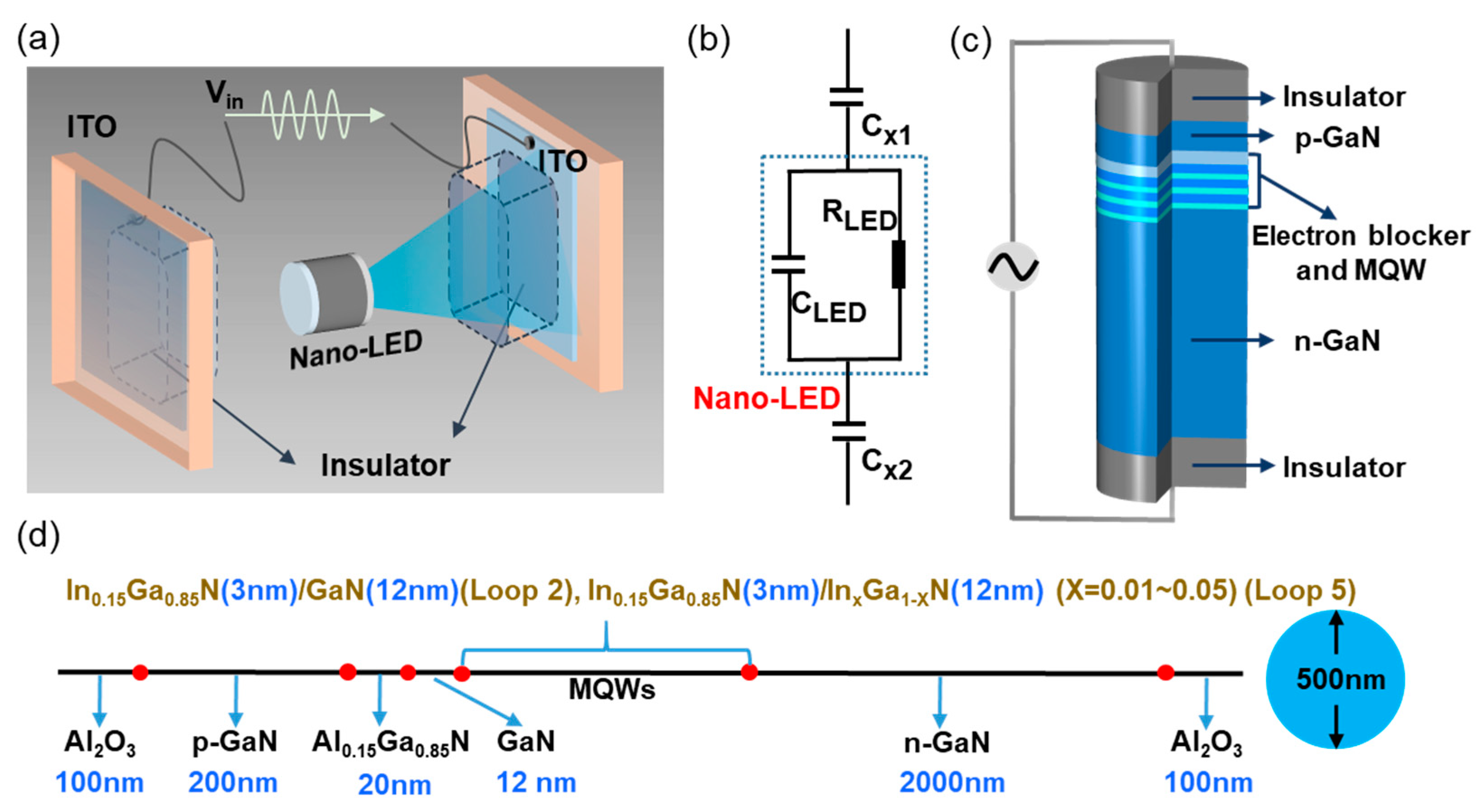
2. Model Details
3. Results and Discussion
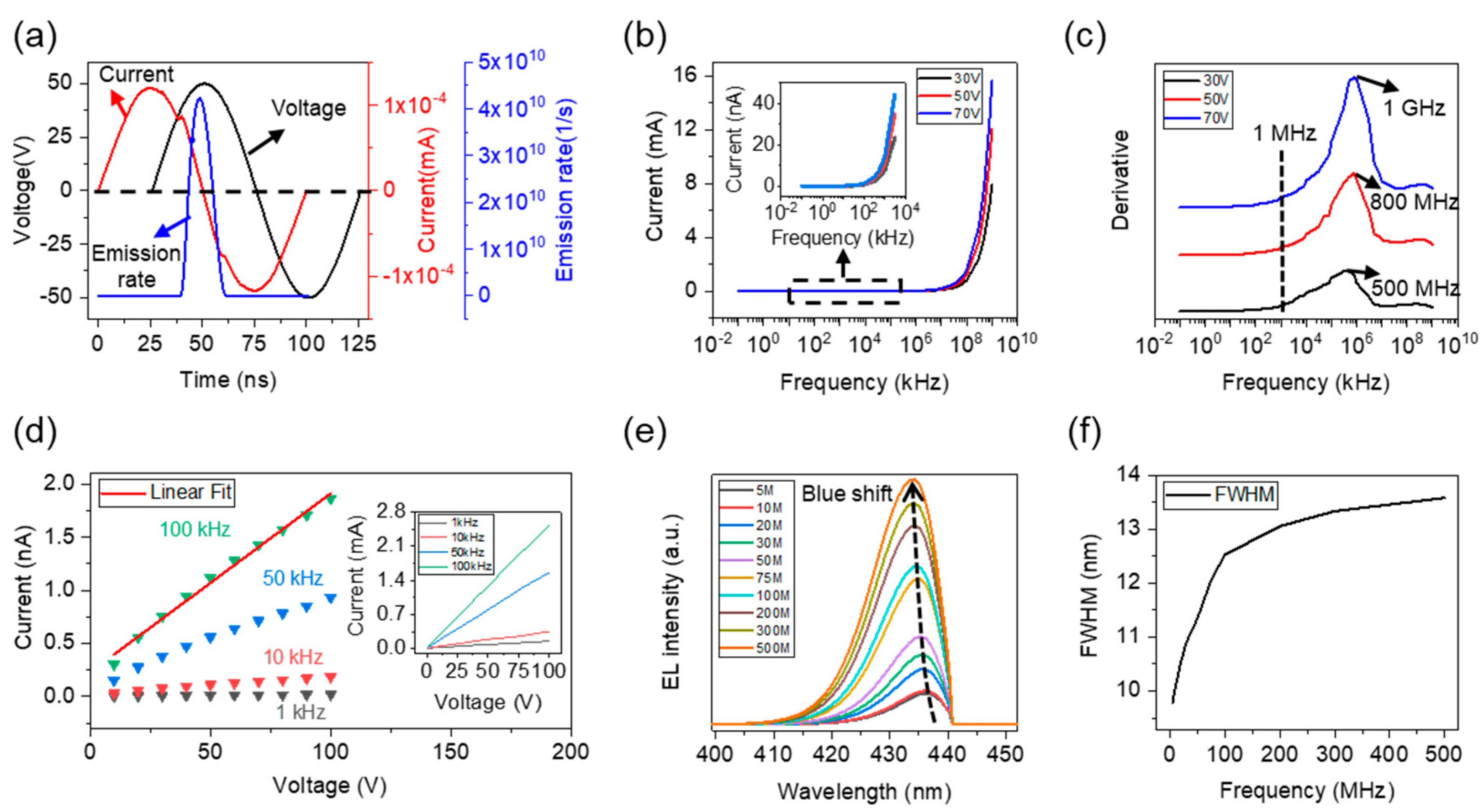
3.1. Typical Electrical and Optical Properties
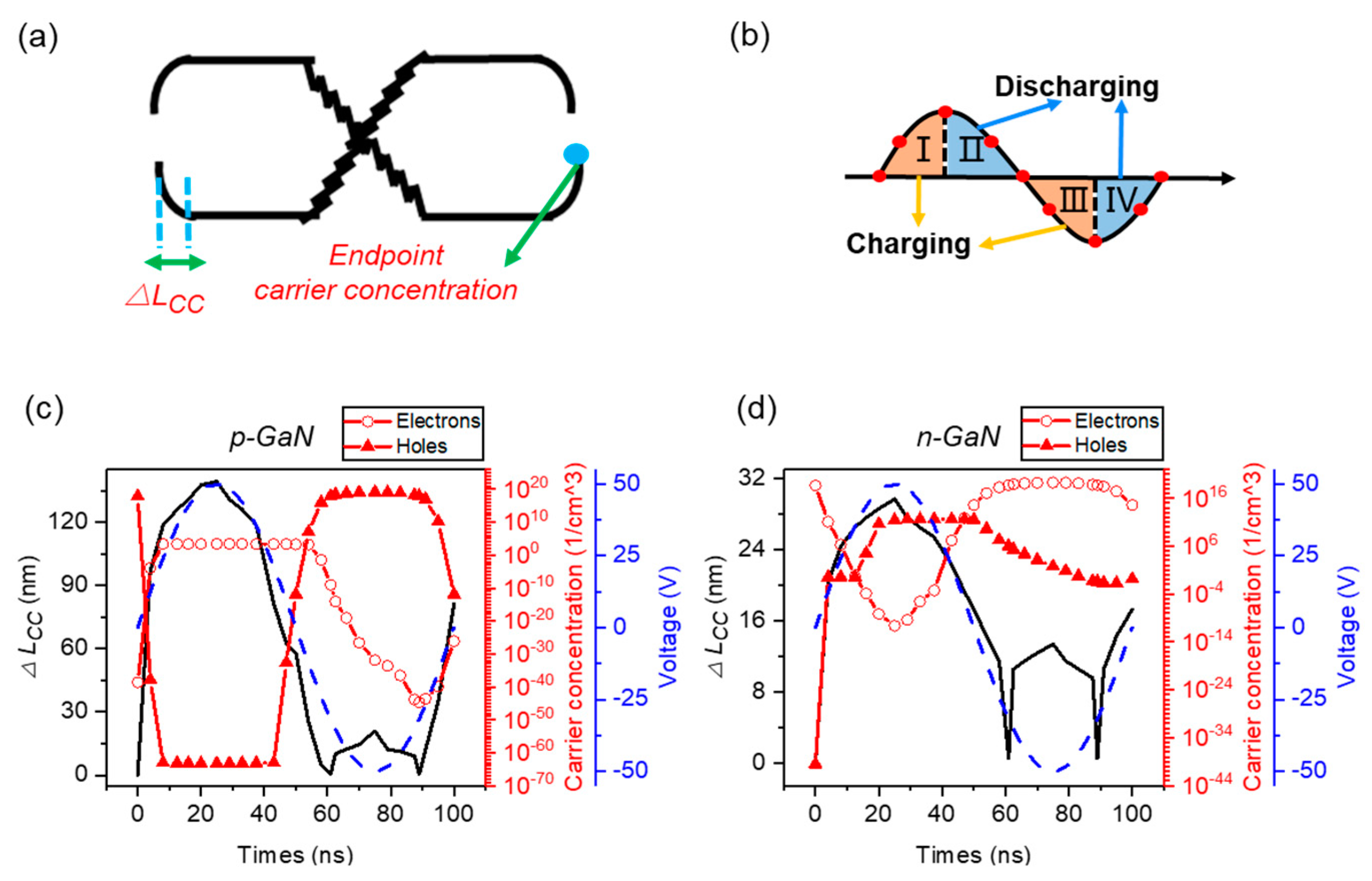
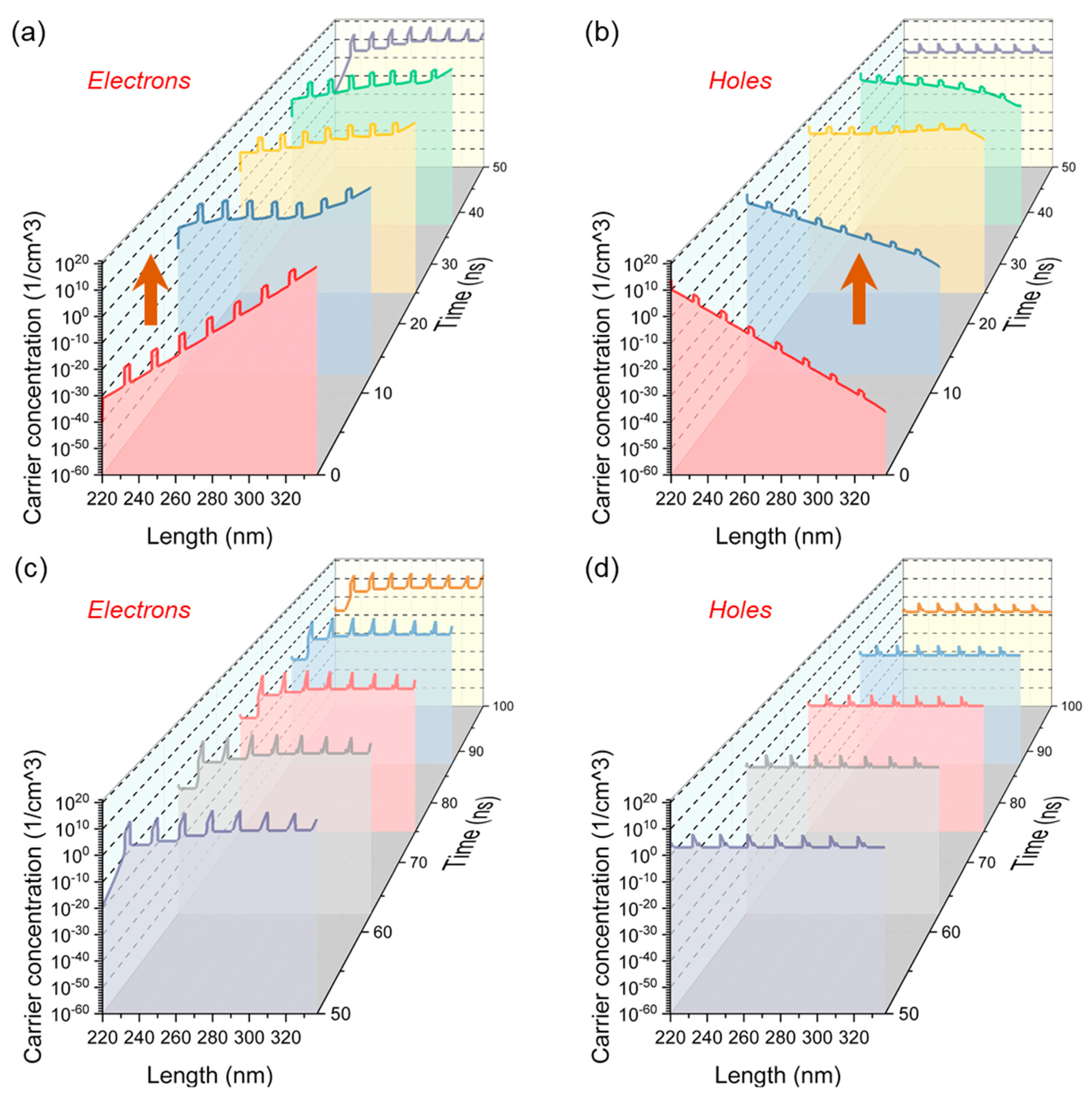
3.2. The Mechanism of Carrier Transport
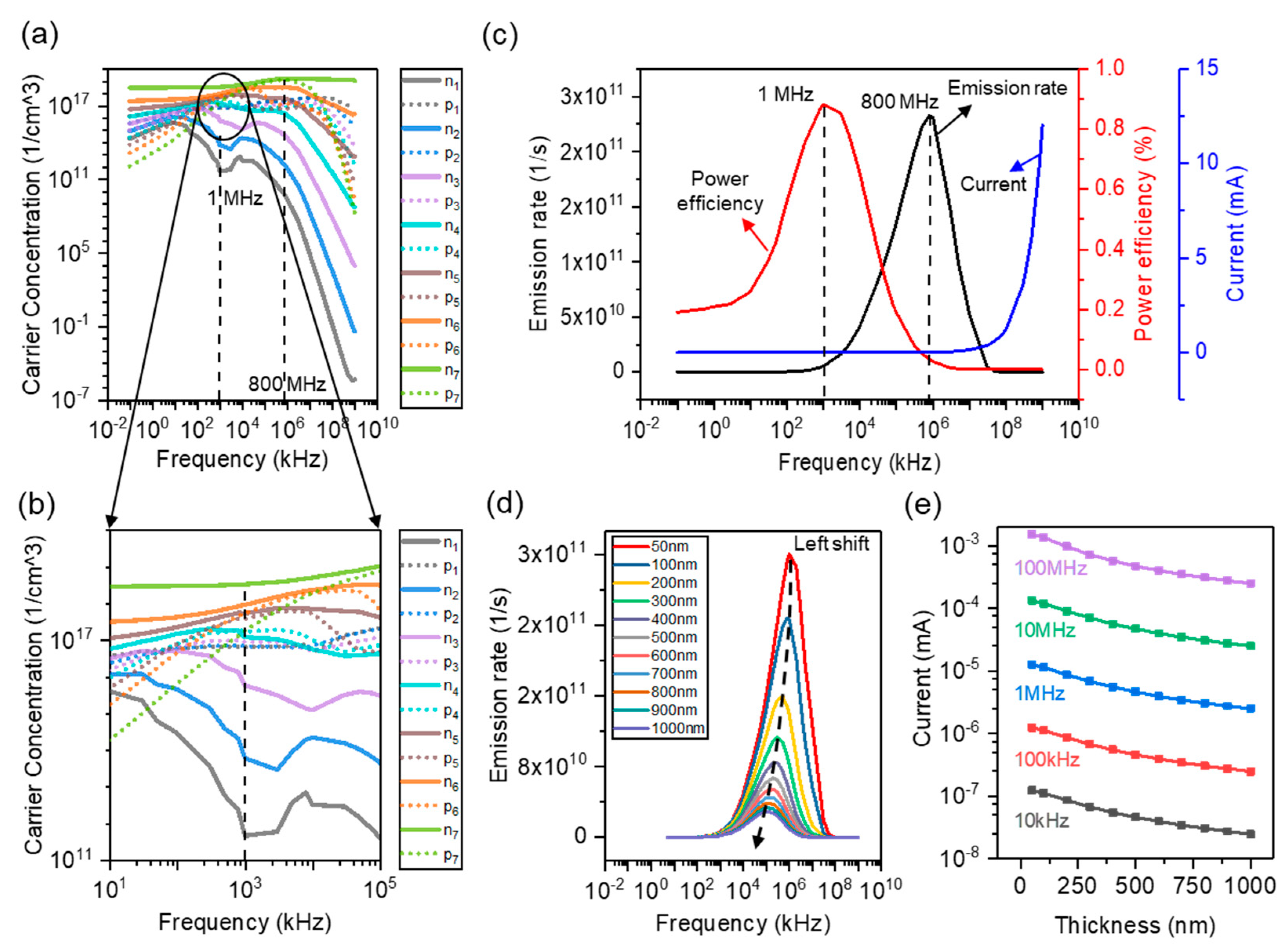
3.3. Frequency Response Characteristics
4. Conclusions
Author Contributions
Funding
Data Availability Statement
Conflicts of Interest
References
- Wang, C.H.; Huang, Y.W.; Wu, S.E.; Liu, C.P. Is it viable to improve light output efficiency by nano-light-emitting diodes? Appl. Phys. Lett. 2013, 103, 351. [Google Scholar] [CrossRef]
- Ra, Y.H.; Wang, R.J.; Woo, S.Y.; Djavid, M.; Sadaf, S.M.; Lee, J.; Botton, G.A.; Mi, Z.T. Full-Color Single Nanowire Pixels for Projection Displays. Nano Lett. 2016, 16, 4608–4615. [Google Scholar] [CrossRef]
- Pan, C.F.; Dong, L.; Zhu, G.; Niu, S.M.; Yu, R.M.; Yang, Q.; Liu, Y.; Wang, Z.L. High-resolution electroluminescent imaging of pressure distribution using a piezoelectric nanowire LED array. Nat. Photonics 2013, 7, 752–758. [Google Scholar] [CrossRef]
- Wasisto, H.S.; Prades, J.D.; Gulink, J.; Waag, A. Beyond solid-state lighting: Miniaturization, hybrid integration, and applications of GaN nano- and micro-LEDs. Appl. Phys. Rev. 2019, 6, 041315. [Google Scholar] [CrossRef] [Green Version]
- Bui, H.Q.T.; Velpula, R.T.; Jain, B.; Aref, O.H.; Nguyen, H.D.; Lenka, T.R.; Nguyen, H.P.T. Full-Color InGaN/AlGaN Nanowire Micro Light-Emitting Diodes Grown by Molecular Beam Epitaxy: A Promising Candidate for Next Generation Micro Displays. Micromachines 2019, 10, 492. [Google Scholar] [CrossRef] [PubMed] [Green Version]
- Chen, F.; Ji, X.H.; Lau, S.P. Recent progress in group III-nitride nanostructures: From materials to applications. Mater. Sci. Eng. R 2020, 142, 100578. [Google Scholar] [CrossRef]
- Wu, C.X.; Wang, K.; Zhang, Y.G.; Zhou, X.T.; Guo, T.L. Emerging Nanopixel Light-Emitting Displays: Significance, Challenges, and Prospects. J. Phys. Chem. Lett. 2021, 12, 3522–3527. [Google Scholar] [CrossRef] [PubMed]
- Kang, J.H.; Li, B.J.; Zhao, T.S.; Johar, M.A.; Lin, C.C.; Fang, Y.H.; Kuo, W.H.; Liang, K.L.; Hu, S.; Ryu, S.W.; et al. RGB Arrays for Micro-Light-Emitting Diode Applications Using Nanoporous GaN Embedded with Quantum Dots. ACS Appl. Mater. Interfaces 2020, 12, 30890–30895. [Google Scholar] [CrossRef] [PubMed]
- Liang, K.L.; Kuo, W.H.; Shen, H.T.; Yu, P.W.; Fang, Y.H.; Lin, C.C. Advances in color-converted micro-LED arrays. Jpn. J. Appl. Phys. 2021, 60, SA0802. [Google Scholar] [CrossRef]
- Wang, K.; Liu, Y.; Wu, C.X.; Li, D.L.; Lv, S.H.; Zhang, Y.G.; Zhou, X.T.; Guo, T.L. Electroluminescence from mu LED without external charge injection. Sci. Rep. 2020, 10, 8059. [Google Scholar] [CrossRef]
- Wang, K.; Chen, P.Q.; Chen, J.J.; Liu, Y.; Wu, C.X.; Sun, J.; Zhou, X.T.; Zhang, Y.A.; Guo, T.L. Alternating current electroluminescence from GaN-based nanorod light-emitting diodes. Opt. Laser Technol. 2021, 140, 107044. [Google Scholar] [CrossRef]
- Chen, P.Q.; Wang, K.; Chen, J.J.; Xu, H.L.; Zhang, Y.A.; Wu, C.X.; Zhou, X.T.; Liu, Z.Q.; Guo, T.L. Achieving Wide Operating Voltage Windows in Non-Carrier Injection Micro-LEDs for Enhancing Luminance Robustness. IEEE Trans. Electron Devices 2021, 69, 212–215. [Google Scholar] [CrossRef]
- Wang, K.; Liu, Y.; Chen, R.; Wu, C.X.; Zhou, X.T.; Zhang, Y.A.; Liu, Z.Q.; Guo, T.L. Light-Pulse Splitting From Nano-Light-Emitting Diodes Operating in Noncarrier Injection Mode. IEEE Electron Device Lett. 2021, 42, 1033–1036. [Google Scholar] [CrossRef]
- Chang, K.P.; Jheng, J.Y.; Huang, S.Y.; Wang, W.K.; Horng, R.H.; Wuu, D.S. Improvement of p-electrode structures for 280 nm AlGaN LED applications. Semicond. Sci. Tech. 2020, 35, 105023. [Google Scholar] [CrossRef]
- Ezshlyakh, D.D.; Spende, H.; Weimann, T.; Hinze, P.; Bornemann, S.; Gulink, J.; Canals, J.; Prades, J.D.; Dieguez, A.; Waag, A. Directly addressable GaN-based nano-LED arrays: Fabrication and electro-optical characterization. Microsyst. Nanoeng. 2020, 6, 88. [Google Scholar] [CrossRef] [PubMed]
- Zhou, S.J.; Liu, X.T.; Yan, H.; Chen, Z.W.; Liu, Y.C.; Liu, S. Highly efficient gan-based high-power flip-chip light-emitting diodes. Opt. Express 2019, 27, A669. [Google Scholar] [CrossRef] [PubMed]
- Zhou, S.J.; Liu, X.T.; Gao, Y.L.; Liu, Y.C.; Liu, M.L.; Liu, Z.Y.; Gui, C.Q.; Liu, S. Numerical and experimental investigation of GaN-based flip-chip light-emitting diodes with highly reflective Ag/TiW and ITO/DBR Ohmic contacts. Opt. Express 2017, 25, 26615–26627. [Google Scholar] [CrossRef] [PubMed]
- Kim, T.K.; Yoon, Y.J.; Oh, S.K.; Lee, Y.L.; Cha, Y.J.; Kwak, J.A. Ohmic contact mechanism for RF superimposed DC sputtered-ITO transparent p-electrodes with a variety of Sn2O3 content for GaN-based light-emitting diodes. Appl. Surf. Sci. 2017, 432, 233–240. [Google Scholar] [CrossRef]
- Wu, N.; Xiong, Z.; Qin, Z. Effect of interfacial composition on Ag-based Ohmic contact of GaN-based vertical light emitting diodes. J. Appl. Phys. 2018, 123, 055301. [Google Scholar] [CrossRef] [Green Version]
- Singh, K.; Chauhan, A.; Mathew, M.; Punia, R.; Meena, S.S.; Gupta, N.; Kundu, R.S. Formation of non-alloyed Ti/Al/Ni/Au low-resistance ohmic contacts on reactively ion-etched n-type GaN by surface treatment for GaN light-emitting diodes applications. Appl. Phys. A 2019, 125, 24. [Google Scholar] [CrossRef]
- Park, W.I.; Yi, G.C. Electroluminescence in n-ZnO nanorod arrays vertically grown on p-GaN. Adv. Mater. 2004, 16, 87–90. [Google Scholar] [CrossRef]
- Eo, Y.J.; Yoo, G.Y.; Kang, H.; Lee, Y.K.; Kim, C.S.; Oh, J.H.; Lee, K.N.; Kim, W.; Do, Y.R. Enhanced DC-Operated Electroluminescence of Forwardly Aligned p/MQW/n InGaN Nanorod LEDs via DC Offset-AC Dielectrophoresis. ACS Appl. Mater. Interfaces 2017, 9, 37912–37920. [Google Scholar] [CrossRef]
- Zhao, X.Y.; Wan, Z.H.; Gong, L.Y.; Tao, G.Y.; Zhou, S.J. Enhanced Optoelectronic Performance of Yellow Light-Emitting Diodes Grown on InGaN/GaN Pre-Well Structure. Nanomaterials 2021, 11, 3231. [Google Scholar] [CrossRef] [PubMed]
- Nee, T.E.; Wang, J.C.; Zhong, B.Y.; Hsiao, J.J.; Wu, Y.F. Thermophysical Characterization of Efficiency Droop in GaN-Based Light-Emitting Diodes. Nanomaterials 2021, 11, 1449. [Google Scholar] [CrossRef]
- Jeong, S.; Oh, S.K.; Ryou, J.H.; Ahn, K.S.; Song, K.M.; Kim, H. Monolithic Inorganic ZnO/GaN Semiconductors Heterojunction White Light-Emitting Diodes. ACS Appl. Mater. Interfaces 2018, 10, 3761–3768. [Google Scholar] [CrossRef]
- Nami, M.; Rashidi, A.; Monavarian, M.; Mishkat-Ul-Masabih, S.; Rishinaramangalam, A.K.; Brueck, S.R.J.; Feezell, D. Electrically Injected GHz-Class GaN/InGaN Core-Nanowire-Based mu LEDs: Carrier Dynamics and Nanoscale Homogeneity. ACS Photonics 2019, 6, 1618–1625. [Google Scholar] [CrossRef]
- Ju, Z.G.; Liu, W.; Zhang, Z.H.; Tan, S.T.; Ji, Y.; Kyaw, Z.; Zhang, X.L.; Lu, S.P.; Zhang, Y.P.; Zhu, B.B.; et al. Advantages of the Blue InGaN/GaN Light-Emitting Diodes with an AlGaN/GaN/AlGaN Quantum Well Structured Electron Blocking Layer. ACS Photonics 2014, 1, 377–381. [Google Scholar] [CrossRef] [Green Version]
- Sadaf, S.M.; Ra, Y.H.; Nguyen, H.P.T.; Djavid, M.; Mi, Z. Alternating-Current InGaN/GaN Tunnel Junction Nanowire White-Light Emitting Diodes. Nano Lett. 2015, 15, 6696–6701. [Google Scholar] [CrossRef] [PubMed]
- Zhang, T.; Yang, P.; Li, Y.Z.; Cao, Y.Z.; Zhou, Y.L.; Chen, M.Z.; Zhu, Z.Q.; Chen, W.M.; Zhou, X.Y. Flexible Transparent Sliced Veneer for Alternating Current Electroluminescent Devices. ACS Sustain. Chem. Eng. 2019, 7, 11464–11473. [Google Scholar] [CrossRef]
- Wang, L.; Xiao, L.; Gu, H.S.; Sun, H.D. Advances in Alternating Current Electroluminescent Devices. Adv. Opt. Mater. 2019, 7, 1801154. [Google Scholar] [CrossRef] [Green Version]
- Liu, Y.; Wang, K.; Wu, C.X.; Park, J.H.; Lin, Z.X.; Zhang, Y.A.; Zhou, X.T.; Guo, T.L.; Kim, T.W. Triboelectric-nanogenerator-inspired light-emitting diode-in-capacitors for flexible operation in high-voltage and wireless drive modes. Nano Energy 2020, 78, 105281. [Google Scholar] [CrossRef]
- Sarwar, T.; Cheekati, S.; Chung, K.; Ku, P.C. On-chip optical spectrometer based on GaN wavelength-selective nanostructural absorbers. Appl. Phys. Lett. 2020, 116, 081103. [Google Scholar] [CrossRef]
- Neugebauer, S.; Metzner, S.; Blasing, J.; Bertram, F.; Dadgar, A.; Christen, J.; Strittmatter, A. Polarization engineering of c-plane InGaN quantum wells by pulsed-flow growth of AlInGaN barriers. Phys. Status Solidi B 2016, 253, 118–125. [Google Scholar] [CrossRef]
- Khan, M.A.; Itokazu, Y.; Maeda, N.; Jo, M.; Yamada, Y.; Hirayama, H. External Quantum Efficiency of 6.5% at 300 nm Emission and 4.7% at 310 nm Emission on Bare Wafer of AlGaN-Based UVB LEDs. ACS Appl. Electron. Mater. 2020, 2, 1892–1907. [Google Scholar] [CrossRef]
- Chen, M.X.; Pan, C.F.; Zhang, T.P.; Li, X.Y.; Liang, R.R.; Wang, Z.L. Tuning Light Emission of a Pressure-Sensitive Silicon/ZnO Nanowires Heterostructure Matrix through Piezo-phototronic Effects. ACS Nano 2016, 10, 6074–6079. [Google Scholar] [CrossRef] [PubMed]
- Perlman, H.; Eisenfeld, T.; Karsenty, A. Performance Enhancement and Applications Review of Nano Light Emitting Device (LED). Nanomaterials 2021, 11, 23. [Google Scholar] [CrossRef]
- Guo, M.; Guo, Z.Y.; Huang, J.; Liu, Y.; Yao, S.Y. Improvement of the carrier distribution with GaN/InGaN/AlGaN/InGaN/ GaN composition-graded barrier for InGaN-based blue light-emitting diode. Chin. Phys. B 2017, 26, 028502. [Google Scholar] [CrossRef]
- Ahmad, S.; Kumar, S.; Kaya, S.; Alvi, P.A.; Siddiqui, M.J. Improvement in efficiency of yellow Light Emitting Diode using InGaN barriers and modified electron injection layer. Optik 2020, 206, 163716. [Google Scholar] [CrossRef]
- Chakraborty, R.; Paul, G.; Pal, A.J. Dynamic Response of Alternating-Current-Driven Light-Emitting Diodes Based on Hybrid Halide Perovskites. Phys. Rev. Appl. 2020, 14, 024006. [Google Scholar] [CrossRef]
- Huang, S.W.; Huang, Y.M.; Chang, Y.H.; Lin, Y.; Liou, F.J.; Hsu, Y.C.; Song, J.; Choi, J.; Chow, C.W.; Lin, C.C.; et al. High-Bandwidth Green Semipolar (20–21) InGaN/GaN Micro Light-Emitting Diodes for Visible Light Communication. ACS Photonics 2020, 7, 2228–2235. [Google Scholar]


| Materials | Band Gap /V | Electron Affinity /V | Electron Mobility/(cm2/(V × s)) | Hole Mobility/(cm2/(V × s)) | Doping Concentration/(1/cm3) |
|---|---|---|---|---|---|
| p-GaN | 3.4 | 4.1 | 1000 | 350 | 7 × 10¹⁷ |
| n-GaN | 3.4 | 4.1 | 1000 | 350 | 5 × 10¹⁸ |
| In0.01Ga0.99N | 3.35884 | 4.12881 | 1000 | 350 | / |
| In0.02Ga0.98N | 3.31797 | 4.15742 | 1000 | 350 | / |
| In0.03Ga0.97N | 3.27739 | 4.18583 | 1000 | 350 | / |
| In0.04Ga0.96N | 3.23709 | 4.21404 | 1000 | 350 | / |
| In0.05Ga0.95N | 3.19708 | 4.24205 | 1000 | 350 | / |
| In0.15Ga0.85N | 2.81268 | 4.51113 | 1000 | 350 | / |
| Al0.15Ga0.85N | 3.693 | 3.575 | 1000 | 350 | 7 × 10¹⁷ |
Publisher’s Note: MDPI stays neutral with regard to jurisdictional claims in published maps and institutional affiliations. |
© 2022 by the authors. Licensee MDPI, Basel, Switzerland. This article is an open access article distributed under the terms and conditions of the Creative Commons Attribution (CC BY) license (https://creativecommons.org/licenses/by/4.0/).
Share and Cite
Li, W.; Wang, K.; Li, J.; Wu, C.; Zhang, Y.; Zhou, X.; Guo, T. Working Mechanisms of Nanoscale Light-Emitting Diodes Operating in Non-Electrical Contact and Non-Carrier Injection Mode: Modeling and Simulation. Nanomaterials 2022, 12, 912. https://doi.org/10.3390/nano12060912
Li W, Wang K, Li J, Wu C, Zhang Y, Zhou X, Guo T. Working Mechanisms of Nanoscale Light-Emitting Diodes Operating in Non-Electrical Contact and Non-Carrier Injection Mode: Modeling and Simulation. Nanomaterials. 2022; 12(6):912. https://doi.org/10.3390/nano12060912
Chicago/Turabian StyleLi, Wenhao, Kun Wang, Junlong Li, Chaoxing Wu, Yongai Zhang, Xiongtu Zhou, and Tailiang Guo. 2022. "Working Mechanisms of Nanoscale Light-Emitting Diodes Operating in Non-Electrical Contact and Non-Carrier Injection Mode: Modeling and Simulation" Nanomaterials 12, no. 6: 912. https://doi.org/10.3390/nano12060912