
Observation of Strong Interlayer Couplings in WS2/MoS2 Heterostructures via Low-Frequency Raman Spectroscopy


Abstract
:1. Introduction
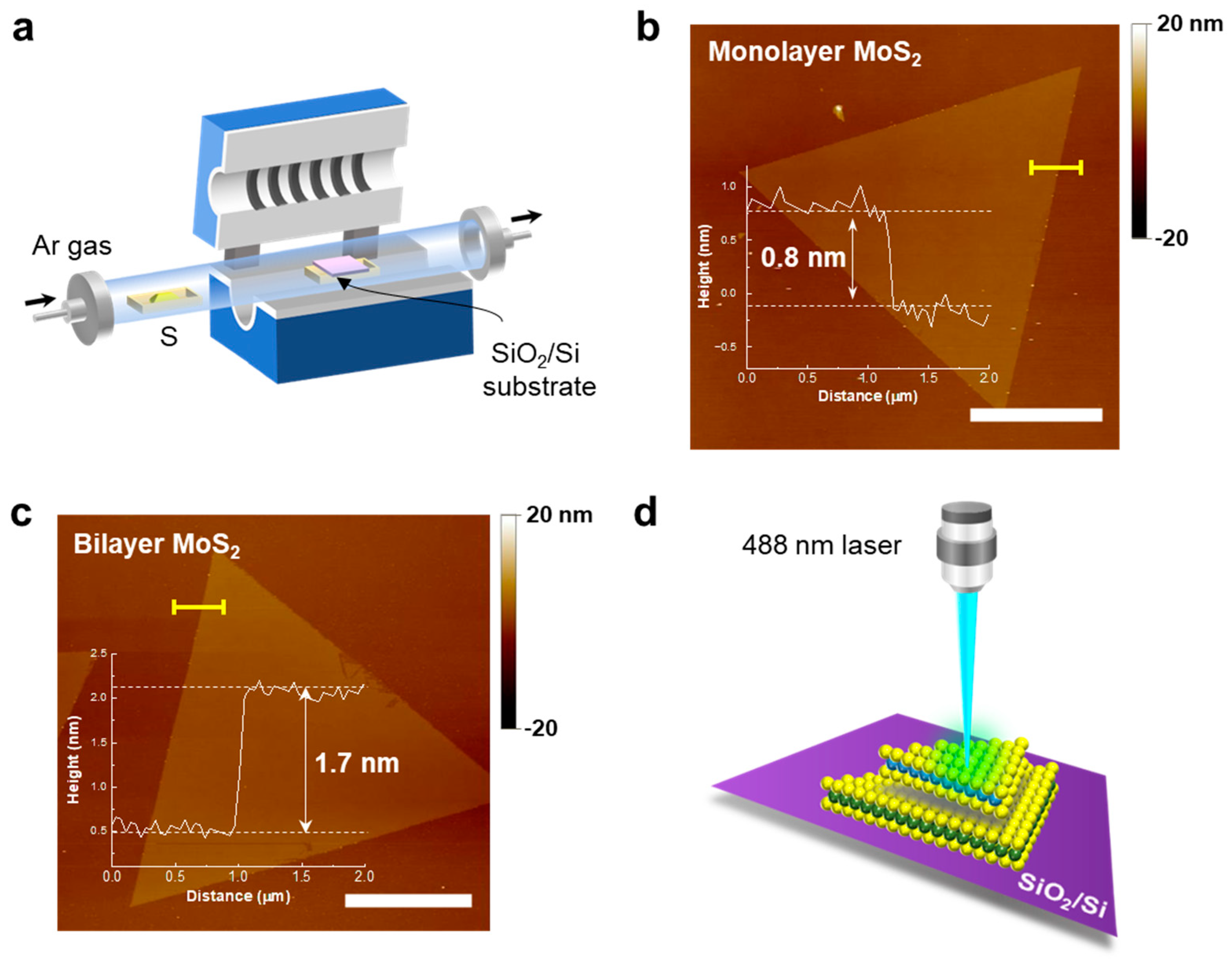
2. Materials and Methods
2.1. Sample Preparation
2.2. Characterization
3. Results and Discussion
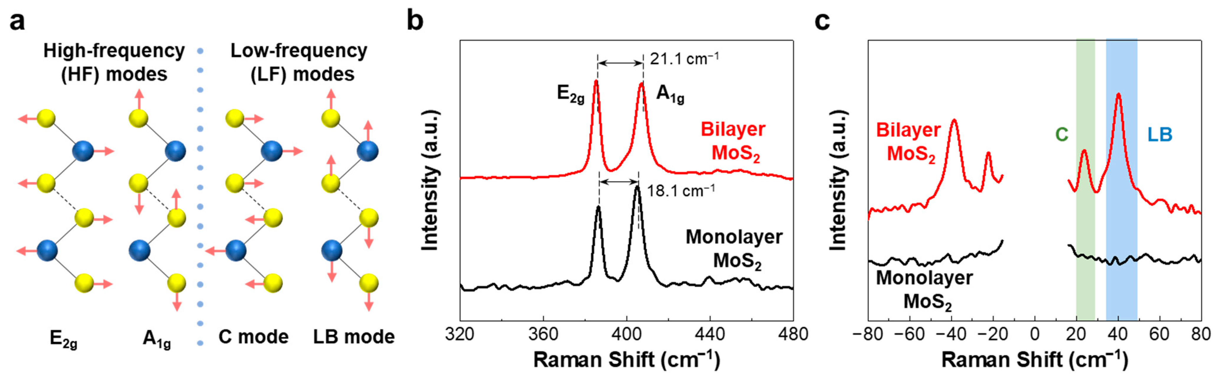
3.1. MoS2 Bilayers
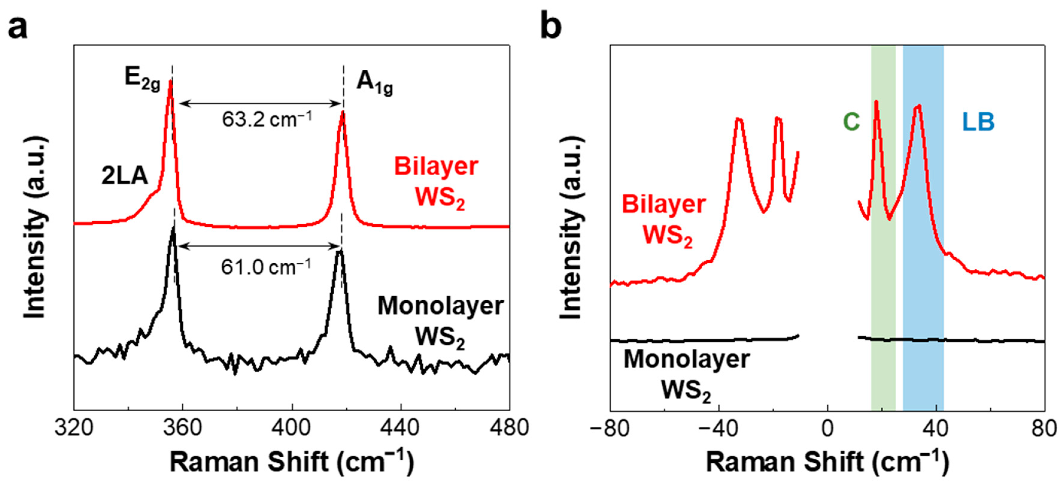
3.2. WS2 Bilayers
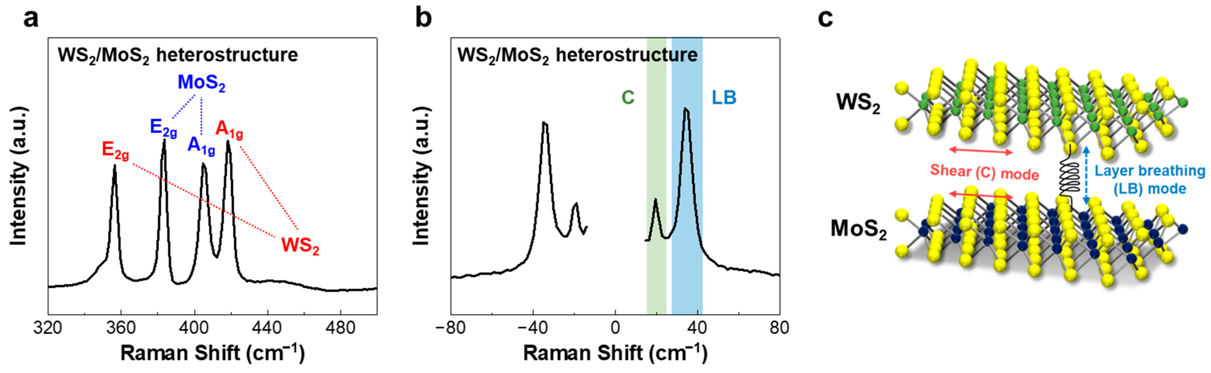
3.3. WS2/MoS2 Heterostructures
4. Conclusions
Author Contributions
Funding
Data Availability Statement
Conflicts of Interest
References
- Manzeli, S.; Ovchinnikov, D.; Pasquier, D.; Yazyev, O.V.; Kis, A. 2D transition metal dichalcogenides. Nat. Rev. Mater. 2017, 2, 17033. [Google Scholar] [CrossRef]
- Fuhrer, M.S.; Hone, J. Measurement of mobility in dual-gated MoS2 Transistors. Nat. Nanotechnol. 2013, 8, 146–147. [Google Scholar] [CrossRef] [PubMed] [Green Version]
- Lee, J.; Pak, S.; Lee, Y.W.; Cho, Y.; Hong, J.; Giraud, P.; Shin, H.S.; Morris, S.M.; Sohn, J.I.; Cha, S.N.; et al. Monolayer optical memory cells based on artificial trap-mediated charge storage and release. Nat. Commun. 2017, 8, 14734. [Google Scholar] [CrossRef] [PubMed] [Green Version]
- Choi, W.; Choudhary, N.; Han, G.H.; Park, J.; Akinwande, D.; Lee, Y.H. Recent development of two-dimensional transition metal dichalcogenides and their applications. Mater. Today 2017, 20, 116–130. [Google Scholar] [CrossRef]
- Liu, X.; Galfsky, T.; Sun, Z.; Xia, F.; Lin, E.C.; Lee, Y.H.; Kéna-Cohen, S.; Menon, V.M. Strong light-matter coupling in two-dimensional atomic crystals. Nat. Photonics 2014, 9, 30–34. [Google Scholar] [CrossRef]
- Pak, S.; Lee, J.; Jang, A.-R.; Kim, S.; Park, K.-H.; Sohn, J.I.; Cha, S. Strain-engineering of contact energy barriers and photoresponse behaviors in monolayer. Adv. Funct. Mater. 2020, 30, 2002023. [Google Scholar] [CrossRef]
- van der Zande, A.M.; Huang, P.Y.; Chenet, D.A.; Berkelbach, T.C.; You, Y.; Lee, G.H.; Heinz, T.F.; Reichman, D.R.; Muller, D.A.; Hone, J.C. Grains and grain boundaries in highly crystalline monolayer molybdenum disulphide. Nat. Mater. 2013, 12, 554–561. [Google Scholar] [CrossRef] [Green Version]
- Bilgin, I.; Liu, F.; Vargas, A.; Winchester, A.; Man, M.K.L.; Upmanyu, M.; Dani, K.M.; Gupta, G.; Talapatra, S.; Mohite, A.D.; et al. Chemical vapor deposition synthesized atomically thin molybdenum disulfide with optoelectronic-grade crystalline quality. ACS Nano 2015, 9, 8822–8832. [Google Scholar] [CrossRef] [Green Version]
- Voiry, D.; Yamaguchi, H.; Li, J.; Silva, R.; Alves, D.C.B.; Fujita, T.; Chen, M.; Asefa, T.; Shenoy, V.B.; Eda, G.; et al. Enhanced catalytic activity in strained chemically exfoliated WS2 nanosheets for hydrogen evolution. Nat. Mater. 2013, 12, 850–855. [Google Scholar] [CrossRef]
- Lee, D.; Jang, A.R.; Kim, J.Y.; Lee, G.; Jung, D.W.; Lee, T.I.; Lee, J.O.; Kim, J.J. Phase-dependent gas sensitivity of MoS2 chemical sensors investigated with phase-locked MoS2. Nanotechnology 2020, 31, 225504. [Google Scholar] [CrossRef]
- Huang, H.; Cui, Y.; Li, Q.; Dun, C.; Zhou, W.; Huang, W.; Chen, L.; Hewitt, C.A.; Carroll, D.L. Metallic 1T phase MoS2 nanosheets for high-performance thermoelectric energy harvesting. Nano Energy 2016, 26, 172–179. [Google Scholar] [CrossRef]
- Yu, X.; Chen, X.; Ding, X.; Yu, X.; Zhao, X.; Chen, X. Facile fabrication of flower-like MoS2/nanodiamond nanocomposite toward high-performance humidity detection. Sens. Actuators B Chem. 2020, 317, 128168. [Google Scholar] [CrossRef]
- Zhao, Z.; Hu, Z.; Li, Q.; Li, H.; Zhang, X.; Zhuang, Y.; Wang, F.; Yu, G. Designing two-dimensional WS2 layered cathode for high-performance aluminum-ion batteries: From micro-assemblies to insertion mechanism. Nano Today 2020, 32, 100870. [Google Scholar] [CrossRef]
- Lee, J.; Pak, S.; Giraud, P.; Lee, Y.-W.; Cho, Y.; Hong, J.; Jang, A.R.; Chung, H.-S.; Hong, W.-K.; Jeong, H.Y.; et al. Thermodynamically stable synthesis of large-scale and highly crystalline transition metal dichalcogenide monolayers and their unipolar n–n heterojunction devices. Adv. Mater. 2017, 29, 1702206. [Google Scholar] [CrossRef]
- Pak, S.; Lee, J.; Lee, Y.W.; Jang, A.R.; Ahn, S.; Ma, K.Y.; Cho, Y.; Hong, J.; Lee, S.; Jeong, H.Y.; et al. Strain-mediated interlayer coupling effects on the excitonic behaviors in an epitaxially Grown MoS2/WS2 van der Waals heterobilayer. Nano Lett. 2017, 17, 5634–5640. [Google Scholar] [CrossRef] [Green Version]
- Duan, X.; Wang, C.; Pan, A.; Yu, R.; Duan, X. Two-dimensional transition metal dichalcogenides as atomically thin semiconductors: Opportunities and challenges. Chem. Soc. Rev. 2015, 44, 8859–8876. [Google Scholar] [CrossRef]
- Zhu, J.; Li, W.; Huang, R.; Ma, L.; Sun, H.; Choi, J.H.; Zhang, L.; Cui, Y.; Zou, G. One-pot selective epitaxial growth of large WS2/MoS2 lateral and vertical heterostructures. J. Am. Chem. Soc. 2020, 142, 16276–16284. [Google Scholar] [CrossRef]
- Wang, S.; Cui, X.; Jian, C.; Cheng, H.; Niu, M.; Yu, J.; Yan, J.; Huang, W. Stacking engineered heterostructures in transition metal dichalcogenides. Adv. Mater. 2021, 33, 2005735. [Google Scholar] [CrossRef]
- Hong, X.; Kim, J.; Shi, S.F.; Zhang, Y.; Jin, C.; Sun, Y.; Tongay, S.; Wu, J.; Zhang, Y.; Wang, F. Ultrafast charge transfer in atomically thin MoS2/WS2 heterostructures. Nat. Nanotechnol. 2014, 9, 682–686. [Google Scholar] [CrossRef] [Green Version]
- Wu, X.; Chen, X.; Yang, R.; Zhan, J.; Ren, Y.; Li, K. Recent Advances on tuning the interlayer coupling and properties in van Der Waals heterostructures. Small 2022, 18, 2105877. [Google Scholar] [CrossRef]
- Gong, Y.; Lin, J.; Wang, X.; Shi, G.; Lei, S.; Lin, Z.; Zou, X.; Ye, G.; Vajtai, R.; Yakobson, B.I.; et al. Vertical and in-plane heterostructures from WS2/MoS2 monolayers. Nat. Mater. 2014, 13, 1135–1142. [Google Scholar] [CrossRef] [PubMed] [Green Version]
- Yan, J.; Ma, C.; Huang, Y.; Yang, G. Tunable control of interlayer excitons in WS2/MoS2 heterostructures via strong coupling with enhanced Mie resonances. Adv. Sci. 2019, 6, 1802092. [Google Scholar] [CrossRef] [PubMed] [Green Version]
- Susarla, S.; Manimunda, P.; Morais Jaques, Y.; Hachtel, J.A.; Idrobo, J.C.; Syed Amnulla, S.A.; Galvão, D.S.; Tiwary, C.S.; Ajayan, P.M. Deformation mechanisms of vertically stacked WS2/MoS2 heterostructures: The role of interfaces. ACS Nano 2018, 12, 4036–4044. [Google Scholar] [CrossRef] [PubMed]
- Tan, H.; Xu, W.; Sheng, Y.; Lau, C.S.; Fan, Y.; Chen, Q.; Tweedie, M.; Wang, X.; Zhou, Y.; Warner, J.H. Lateral graphene-contacted vertically stacked WS2/MoS2 hybrid photodetectors with large Gain. Adv. Mater. 2017, 29, 1702917. [Google Scholar] [CrossRef] [PubMed]
- Wang, G.; Li, L.; Fan, W.; Wang, R.; Zhou, S.; Lü, J.T.; Gan, L.; Zhai, T. Interlayer coupling induced infrared response in WS2/MoS2 heterostructures enhanced by surface plasmon resonance. Adv. Funct. Mater. 2018, 28, 1800339. [Google Scholar] [CrossRef]
- Zhang, X.; Qiao, X.F.; Shi, W.; Wu, J.B.; Jiang, D.S.; Tan, P.H. Phonon and Raman scattering of two-dimensional transition metal dichalcogenides from monolayer, multilayer to bulk material. Chem. Soc. Rev. 2015, 44, 2757–2785. [Google Scholar] [CrossRef] [Green Version]
- Liang, L.; Zhang, J.; Sumpter, B.G.; Tan, Q.H.; Tan, P.H.; Meunier, V. Low-frequency shear and layer-breathing modes in Raman scattering of two-dimensional materials. ACS Nano 2017, 11, 11777–11802. [Google Scholar] [CrossRef]
- Zhang, J.; Wang, J.H.; Chen, P.; Sun, Y.; Wu, S.; Jia, Z.Y.; Lu, X.B.; Yu, H.; Chen, W.; Zhu, J.Q.; et al. Observation of strong interlayer coupling in MoS2/WS2 heterostructures. Adv. Mater. 2016, 28, 1950–1956. [Google Scholar] [CrossRef]
- Zhang, F.; Lu, Z.; Choi, Y.; Liu, H.; Zheng, H.; Xie, L.; Park, K.; Jiao, L.; Tao, C. Atomically resolved observation of continuous interfaces between an as-grown MoS2 monolayer and a WS2/MoS2 heterobilayer on SiO2. ACS Appl. Nano Mater. 2018, 1, 2041–2048. [Google Scholar] [CrossRef] [Green Version]
- Saito, Y.; Kondo, T.; Ito, H.; Okada, M.; Shimizu, T.; Kubo, T.; Kitaura, R. Low frequency Raman study of interlayer couplings in WS2-MoS2 van der Waals heterostructures. Jpn. J. Appl. Phys. 2020, 59, 062004. [Google Scholar] [CrossRef]
- Huang, S.; Liang, L.; Ling, X.; Puretzky, A.A.; Geohegan, D.B.; Sumpter, B.G.; Kong, J.; Meunier, V.; Dresselhaus, M.S. Low-Frequency Interlayer Raman modes to probe interface of twisted bilayer MoS2. Nano Lett. 2016, 16, 1435–1444. [Google Scholar] [CrossRef] [PubMed]
- Lee, J.; Pak, S.; Lee, Y.W.; Park, Y.; Jang, A.R.; Hong, J.; Cho, Y.; Hou, B.; Lee, S.; Jeong, H.Y.; et al. Direct Epitaxial Synthesis of Selective Two-Dimensional Lateral Heterostructures. ACS Nano 2019, 13, 13047–13055. [Google Scholar] [CrossRef] [PubMed]
- Zhao, Y.; Luo, X.; Li, H.; Zhang, J.; Araujo, P.T.; Gan, C.K.; Wu, J.; Zhang, H.; Quek, S.Y.; Dresselhaus, M.S.; et al. Interlayer breathing and shear modes in few-trilayer MoS2 and WSe2. Nano Lett. 2013, 13, 1007–1015. [Google Scholar] [CrossRef] [PubMed] [Green Version]
- Lee, C.; Yan, H.; Brus, L.E.; Heinz, T.F.; Hone, J.; Ryu, S. Anomalous lattice vibrations of single- and few-layer MoS2. ACS Nano 2010, 4, 2695–2700. [Google Scholar] [CrossRef] [PubMed] [Green Version]
- Sun, Y.; Cai, D.; Yang, Z.; Li, H.; Li, Q.; Jia, D.; Zhou, Y. The Preparation, microstructure and mechanical properties of a dense MgO-Al2O3-SiO2 based glass-ceramic coating on porous BN/Si2N2O ceramics. RSC Adv. 2018, 8, 17569–17574. [Google Scholar] [CrossRef] [Green Version]
- Zeng, H.; Zhu, B.; Liu, K.; Fan, J.; Cui, X.; Zhang, Q.M. Low-frequency Raman modes and electronic excitations in atomically thin MoS2 films. Phys. Rev. B 2012, 86, 241301. [Google Scholar] [CrossRef] [Green Version]
- Sam, R.T.; Umakoshi, T.; Verma, P. Probing stacking configurations in a few layered MoS2 by low frequency Raman spectroscopy. Sci. Rep. 2020, 10, 21227. [Google Scholar] [CrossRef]
- Li, H.; Zhang, Q.; Yap, C.C.R.; Tay, B.K.; Edwin, T.H.T.; Olivier, A.; Baillargeat, D. From bulk to monolayer MoS2: Evolution of Raman scattering. Adv. Funct. Mater. 2012, 22, 1385–1390. [Google Scholar] [CrossRef]
- Najmaei, S.; Liu, Z.; Ajayan, P.M.; Lou, J. Thermal effects on the characteristic Raman spectrum of molybdenum disulfide (MoS2) of varying thicknesses. Appl. Phys. Lett. 2012, 100, 013106. [Google Scholar] [CrossRef] [Green Version]
- Puretzky, A.A.; Liang, L.; Li, X.; Xiao, K.; Wang, K.; Mahjouri-Samani, M.; Basile, L.; Idrobo, J.C.; Sumpter, B.G.; Meunier, V.; et al. Low-frequency Raman fingerprints of two-dimensional metal dichalcogenide layer stacking configurations. ACS Nano 2015, 9, 6333–6342. [Google Scholar] [CrossRef]
- Berkdemir, A.; Gutiérrez, H.R.; Botello-Méndez, A.R.; Perea-López, N.; Elías, A.L.; Chia, C.I.; Wang, B.; Crespi, V.H.; López-Urías, F.; Charlier, J.C.; et al. Identification of individual and few layers of WS2 using Raman spectroscopy. Sci. Rep. 2013, 3, 1755. [Google Scholar] [CrossRef] [Green Version]
- Zhao, W.; Ghorannevis, Z.; Amara, K.K.; Pang, J.R.; Toh, M.; Zhang, X.; Kloc, C.; Tan, P.H.; Eda, G. Lattice dynamics in mono- and few-layer sheets of WS2 and WSe2. Nanoscale 2013, 5, 9677–9683. [Google Scholar] [CrossRef] [PubMed] [Green Version]
- Samad, L.; Bladow, S.M.; Ding, Q.; Zhuo, J.; Jacobberger, R.M.; Arnold, M.S.; Jin, S. Layer-controlled chemical vapor deposition growth of MoS2 vertical heterostructures via van der Waals epitaxy. ACS Nano 2016, 10, 7039–7046. [Google Scholar] [CrossRef] [PubMed]
Publisher’s Note: MDPI stays neutral with regard to jurisdictional claims in published maps and institutional affiliations. |
© 2022 by the authors. Licensee MDPI, Basel, Switzerland. This article is an open access article distributed under the terms and conditions of the Creative Commons Attribution (CC BY) license (https://creativecommons.org/licenses/by/4.0/).
Share and Cite
Shin, K.H.; Seo, M.-K.; Pak, S.; Jang, A.-R.; Sohn, J.I. Observation of Strong Interlayer Couplings in WS2/MoS2 Heterostructures via Low-Frequency Raman Spectroscopy. Nanomaterials 2022, 12, 1393. https://doi.org/10.3390/nano12091393
Shin KH, Seo M-K, Pak S, Jang A-R, Sohn JI. Observation of Strong Interlayer Couplings in WS2/MoS2 Heterostructures via Low-Frequency Raman Spectroscopy. Nanomaterials. 2022; 12(9):1393. https://doi.org/10.3390/nano12091393
Chicago/Turabian StyleShin, Ki Hoon, Min-Kyu Seo, Sangyeon Pak, A-Rang Jang, and Jung Inn Sohn. 2022. "Observation of Strong Interlayer Couplings in WS2/MoS2 Heterostructures via Low-Frequency Raman Spectroscopy" Nanomaterials 12, no. 9: 1393. https://doi.org/10.3390/nano12091393