
Promoted Mid-Infrared Photodetection of PbSe Film by Iodine Sensitization Based on Chemical Bath Deposition

Abstract
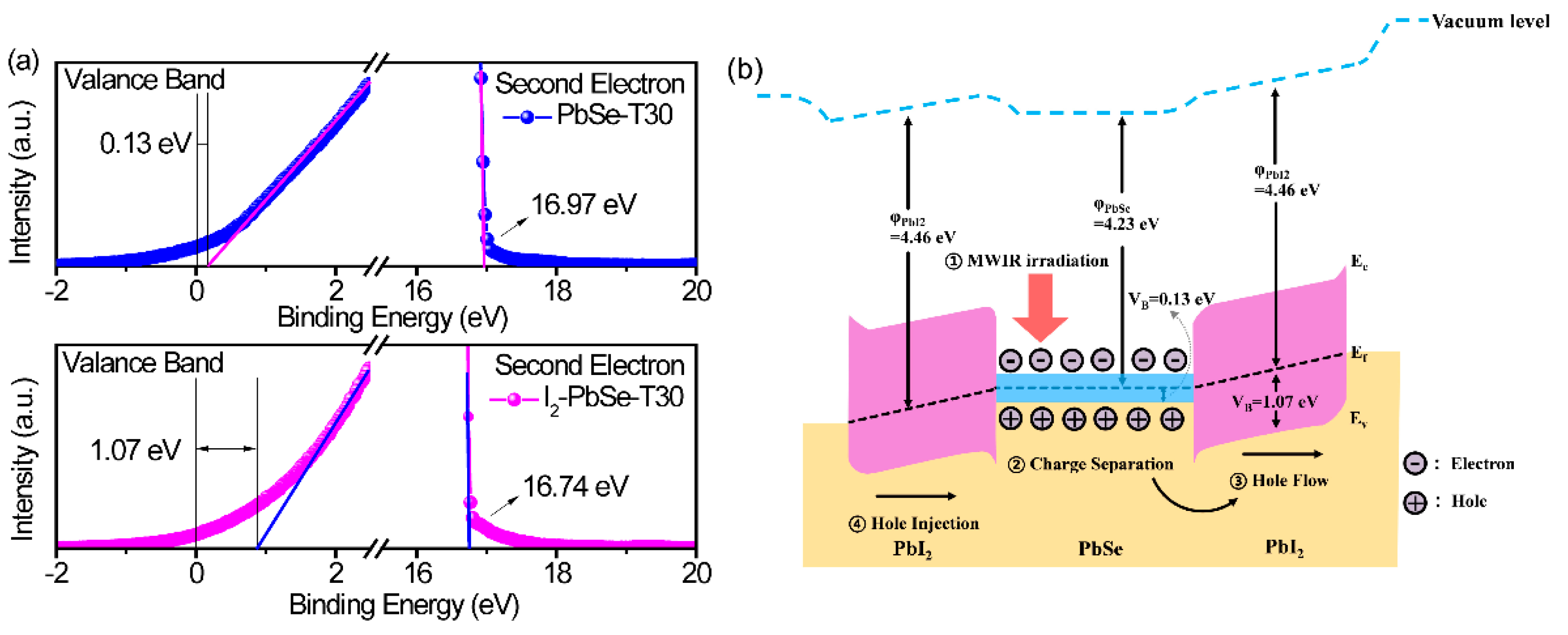
:
1. Introduction
2. Materials and Methods
2.1. Synthesis of PbSe Films
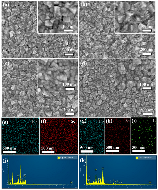
2.2. Materials Characterization
2.3. Device Fabrication
3. Results and Discussion
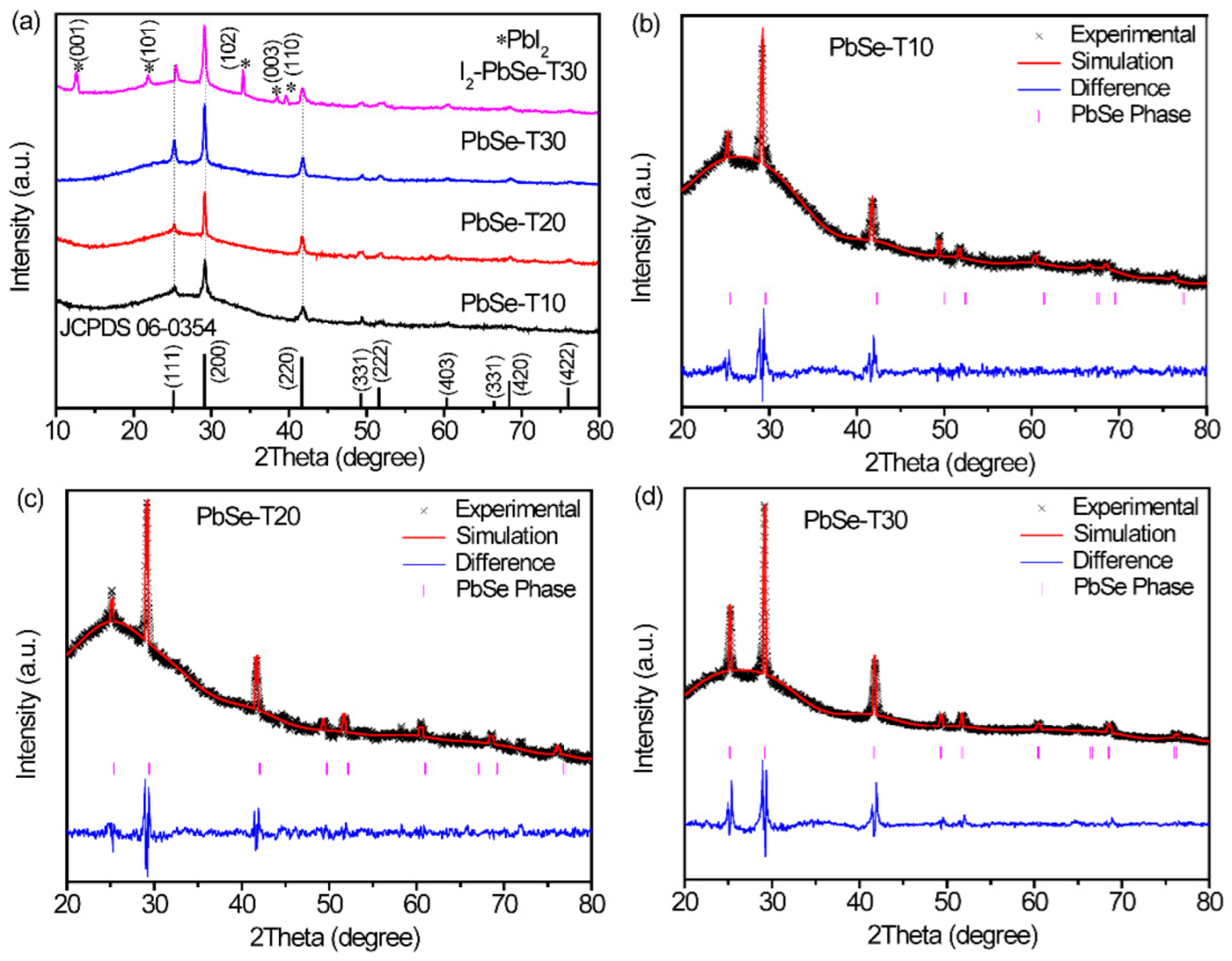
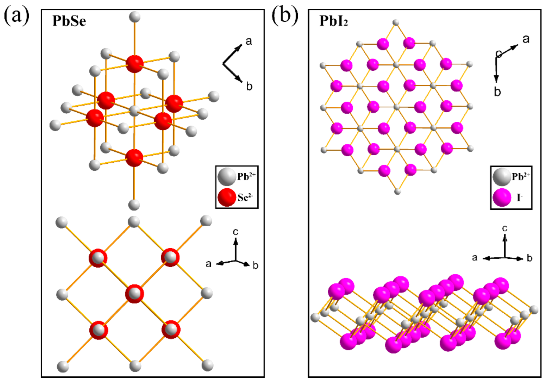
3.1. Structural Data
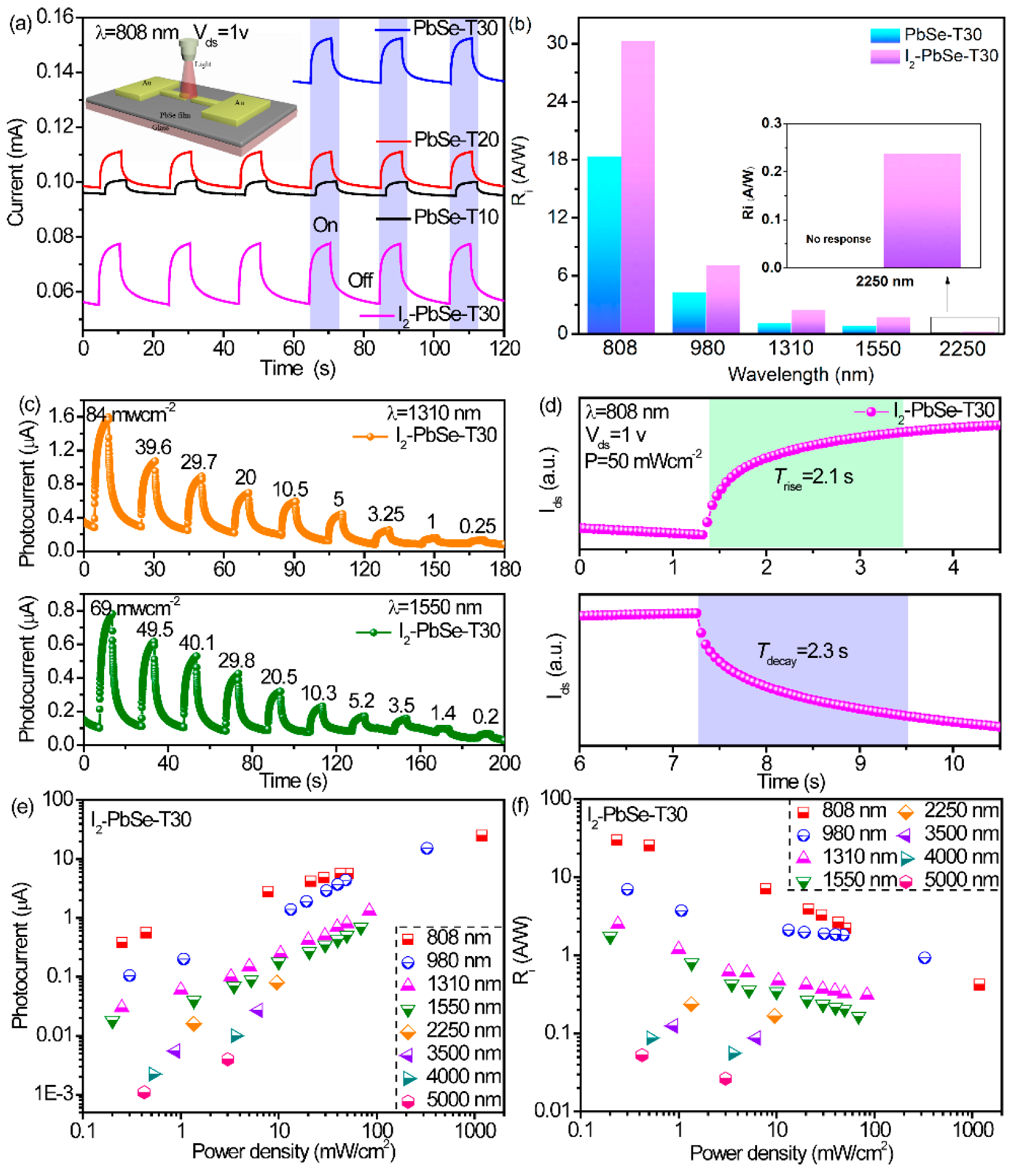
3.2. Photoelectric Properties
4. Conclusions
Supplementary Materials
Author Contributions
Funding
Data Availability Statement
Acknowledgments
Conflicts of Interest
References
- Ren, Z.; Sun, J.; Li, H.; Mao, P.; Wei, Y.; Zhong, X.; Xinhua, Z.; Yang, S.; Wang, J. Bilayer PbS Quantum Dots for High-Performance Photodetectors. Adv. Mater. 2017, 29, 1702055. [Google Scholar] [CrossRef] [PubMed]
- Gong, X.X.; Fei, G.T.; Fu, W.B.; Zhong, B.N.; Gao, X.D.; De Zhang, L. Metal-semiconductor-metal infrared photodetector based on PbTe nanowires with fast response and recovery time. Appl. Surf. Sci. 2017, 404, 7–11. [Google Scholar] [CrossRef]
- Peng, M.; Liu, Y.; Li, F.; Hong, X.; Liu, Y.; Wen, Z.; Liu, Z.; Ma, W.; Sun, X. Room-Temperature Direct Synthesis of PbSe Quantum Dot Inks for High-Detectivity Near-Infrared Photodetectors. ACS Appl. Mater. Interfaces 2021, 13, 51198–51204. [Google Scholar] [CrossRef]
- Harrison, J.T.; Pantoja, E.; Jang, M.-H.; Gupta, M.C. Laser sintered PbSe semiconductor thin films for Mid-IR applications using nanocrystals. J. Alloys Compd. 2020, 849, 156537. [Google Scholar] [CrossRef]
- Hu, L.; Huang, S.; Patterson, R.; Halpert, J.E. Enhanced mobility in PbS quantum dot films via PbSe quantum dot mixing for optoelectronic applications. J. Mater. Chem. C 2019, 7, 4497–4502. [Google Scholar] [CrossRef]
- Nakotte, T.; Luo, H.; Pietryga, J. PbE (E = S, Se) Colloidal Quantum Dot-Layered 2D Material Hybrid Photodetectors. Nanomaterials 2020, 10, 172. [Google Scholar] [CrossRef] [Green Version]
- Dolatyari, M.; Rostami, A.; Mathur, S.; Klein, A. Trap engineering in solution processed PbSe quantum dots for high-speed MID-infrared photodetectors. J. Mater. Chem. C 2019, 7, 5658–5669. [Google Scholar] [CrossRef]
- Yang, C.; Feng, S.; Yu, Y.; Shen, J.; Wei, X.; Shi, H. Electrochemical epitaxial (200) PbSe submicron-plates on single-layer graphene for an ultrafast infrared response. J. Mater. Chem. C 2021, 9, 6536–6543. [Google Scholar] [CrossRef]
- Deng, J.; Lv, W.; Zhang, P.; Huang, W. Large-scale preparation of ultra-long ZnSe-PbSe heterojunction nanowires for flexible broadband photodetectors. J. Sci.-Adv. Mater. Dev. 2021, 7, 100396. [Google Scholar] [CrossRef]
- Han, L.; Balazs, D.M.; Shulga, A.G.; Abdu-Aguye, M.; Ma, W.; Loi, M.A. PbSe Nanorod Field-Effect Transistors: Room- and Low-Temperature Performance. Adv. Electron. Mater. 2018, 4, 1700580. [Google Scholar] [CrossRef] [Green Version]
- Ahmad, W.; He, J.; Liu, Z.; Xu, K.; Chen, Z.; Yang, X.; Li, D.; Xia, Y.; Zhang, J.; Chen, C. Lead Selenide (PbSe) Colloidal Quantum Dot Solar Cells with >10% Efficiency. Adv. Mater. 2019, 31, e1900593. [Google Scholar] [CrossRef] [PubMed]
- Kim, S.; Marshall, A.R.; Kroupa, D.M.; Miller, E.M.; Luther, J.M.; Jeong, S.; Beard, M.C. Air-Stable and Efficient PbSe Quantum-Dot Solar Cells Based upon ZnSe to PbSe Cation-Exchanged Quantum Dots. ACS Nano 2015, 9, 8157–8164. [Google Scholar] [CrossRef] [PubMed]
- Roa, S.; Sandoval, M.; Burgos, M.J.C.; Manidurai, P.; Suárez, S. Potential photovoltaic properties of thin film solar cells based on chemically deposited ZnO/PbSe junctions. J. Alloys Compd. 2021, 871, 159559. [Google Scholar] [CrossRef]
- Yan, L.; Shen, X.; Zhang, Y.; Zhang, T.; Zhang, X.; Feng, Y.; Yin, J.; Zhao, J.; Yu, W.W. Near-infrared light emitting diodes using PbSe quantum dots. RSC Adv. 2015, 5, 54109–54114. [Google Scholar] [CrossRef]
- Ma, Y.; Zhang, Y.; Yu, W.W. Near infrared emitting quantum dots: Synthesis, luminescence properties and applications. J. Mater. Chem. C 2019, 7, 13662–13679. [Google Scholar] [CrossRef]
- Khoshkhoo, M.S.; Zhang, P.; Hiekel, K.; Martín-García, B.; Reichhelm, A.; Lesnyak, V.; Eychmüller, A. Semiconductor Nanocrystal Heterostructures: Near-Infrared Emitting PbSe-Tipped CdSe Tetrapods. Chem. Mater. 2020, 32, 4045–4053. [Google Scholar] [CrossRef]
- Wang, Y.; Hamann, D.M.; Cordova, D.L.M.; Chen, J.; Wang, B.; Shen, L.; Cai, Z.; Shi, H.; Karapetrova, E.; Aravind, I.; et al. Enhanced Low-Temperature Thermoelectric Performance in (PbSe)1+δ(VSe2)1 Heterostructures due to Highly Correlated Electrons in Charge Density Waves. Nano Lett. 2020, 20, 8008–8014. [Google Scholar] [CrossRef]
- Zhou, N.-N.; Hu, Z.-Q.; Nasser, R.; Song, J.-M. Thermoelectric Properties of PbSe Nanocomposites from Solution-Processed Building Blocks. ACS Appl. Energy Mater. 2021, 4, 2014–2019. [Google Scholar] [CrossRef]
- Sun, H.; Cai, B.; Zhao, P.; Yu, F.; Zhang, L.; Yu, D.; Tian, Y.; Xu, B. Enhancement of thermoelectric performance of Al doped PbTe-PbSe due to carrier concentration optimization and alloying. J. Alloys Compd. 2019, 791, 786–791. [Google Scholar] [CrossRef]
- Zhao, M.; Chang, C.; Xiao, Y.; Zhao, L.-D. High performance of n-type (PbS)1-x-y(PbSe)x(PbTe)y thermoelectric materials. J. Alloys Compd. 2018, 744, 769–777. [Google Scholar] [CrossRef]
- Qin, B.; Hu, X.; Zhang, Y.; Wu, H.; Pennycook, S.J.; Zhao, L. Comprehensive Investigation on the Thermoelectric Properties of p-Type PbTe-PbSe-PbS Alloys. Adv. Electron. Mater. 2019, 5, 1900609. [Google Scholar] [CrossRef]
- Ren, Y.; Dai, T.; He, B.; Liu, X. Improvement on performances of graphene-PbSe Schottky photodetector via oxygen-sensitization of PbSe. Mater. Lett. 2019, 236, 194–196. [Google Scholar] [CrossRef]
- Luo, P.; Zhuge, F.; Wang, F.; Lian, L.; Liu, K.; Zhang, J.; Zhai, T. PbSe Quantum Dots Sensitized High-Mobility Bi2O2Se Nanosheets for High-Performance and Broadband Photodetection Beyond 2 μm. ACS Nano 2019, 13, 9028–9037. [Google Scholar] [CrossRef] [PubMed]
- Gupta, M.C.; Harrison, J.T.; Islam, T. Photoconductive PbSe thin films for infrared imaging. Mater. Adv. 2021, 2, 3133–3160. [Google Scholar] [CrossRef]
- Wang, X.J.; Chang, Y.; Hou, Y.B.; Becker, C.R.; Kodama, R.; Aqariden, F.; Sivananthan, S. Molecular beam epitaxy growth of PbSe on Si (211) using a ZnTe buffer layer. J. Vac. Sci. Technol. A 2011, 29, 051503. [Google Scholar] [CrossRef]
- Wang, X.; Hou, Y.; Chang, Y.; Becker, C.; Klie, R.; Kodama, R.; Aqariden, F.; Sivananthan, S. Growth of PbSe on ZnTe/GaAs(211)B by molecular beam epitaxy. J. Cryst. Growth 2010, 312, 910–913. [Google Scholar] [CrossRef]
- Chusnutdinow, S.; Szot, M.; Schreyeck, S.; Aleszkiewicz, M.; Kucherenko, I.; Muratov, A.; Yakovlev, V.; Wojtowicz, T.; Karczewski, G. Ternary Pb1−xCdxSe films grown by molecular beam epitaxy on GaAs/ZnTe hybrid substrates. J. Cryst. Growth 2018, 507, 10–15. [Google Scholar] [CrossRef]
- Virt, I.; Rudyi, I.O.; Lopatynskyi, I.Y.; Dubov, Y.; Tur, Y.; Łusakowska, E.; Luka, G. Growth Mechanisms and Structural Properties of Lead Chalcogenide Films Grown by Pulsed Laser Deposition. J. Electron. Mater. 2017, 46, 175–181. [Google Scholar] [CrossRef] [Green Version]
- Sun, X.; Gao, K.; Pang, X.; Sun, Q.; Li, J. Thermodynamic energy variation diagram to speculate preferred growth orientation of magnetron sputtered PbSe thin films on monocrystalline silicon substrates. Appl. Surf. Sci. 2018, 452, 1–10. [Google Scholar] [CrossRef]
- Wu, W.; Tang, Y.; Li, B.; Xiang, X.; Liu, C.; Zu, X. Microstructure and optical properties of PbSe nanocrystalline films prepared by magnetron sputtering. Opt. Mater. 2021, 118, 111233. [Google Scholar] [CrossRef]
- Hemati, T.; Zhang, X.; Weng, B. A direct oriented-attachment growth of lead-chalcogenide mid-infrared nanocrystals film on amorphous substrates. J. Mater. Chem. C 2020, 8, 13205–13212. [Google Scholar] [CrossRef]
- Jang, M.-H.; Yoo, S.-S.; Kramer, M.T.; Dhar, N.K.; Gupta, M.C. Properties of chemical bath deposited and sensitized PbSe thin films for IR detection. Semicond. Sci. Technol. 2019, 34, 115010. [Google Scholar] [CrossRef]
- Feng, W.; Song, J.; Ren, Y.; Chen, F.; Hu, J.; Yu, S.; Zhao, H.; Tang, Y.; Huang, S. Structural and optical evolution in Pb100-Ag Se (x = 3, 6, 9 and 12) thin films by chemical bath deposition. J. Alloys Compd. 2018, 770, 649–654. [Google Scholar] [CrossRef]
- Das Mahapatra, A.; Basak, D. Biodegradable Filter Paper Based Broad-Band Photodetection by Chemical Bath Deposited SnS2 2D-Nanosheet Array Film. ACS Appl. Electron. Mater. 2021, 3, 2114–2122. [Google Scholar] [CrossRef]
- Yang, H.; Li, X.; Mei, T.; Zheng, J. The lead selenide photoconductive sensitization via oxygen ion implantation with enhanced optical absorption and carrier mobility. J. Mater. Sci. 2017, 52, 10779–10786. [Google Scholar] [CrossRef]
- Yang, H.; Chen, L.; Li, X.; Zheng, J. Intrinsic stoichiometry optimization of polycrystalline lead selenide film in the sensitization process by iodine concentration regulation. Mater. Lett. 2016, 169, 273–277. [Google Scholar] [CrossRef]
- Suh, Y.; Suh, S.-H. Effect of iodine doping in the deposition solution and iodine vapor pressure in the sensitization treatment on the properties of PbSe films. Opt. Eng. 2017, 56, 091607. [Google Scholar] [CrossRef]
- Ganguly, S.; Tang, X.; Yoo, S.-S.; Guyot-Sionnest, P.; Ghosh, A.W. Extrinsic voltage control of effective carrier lifetime in polycrystalline PbSe mid-wave IR photodetectors for increased detectivity. AIP Adv. 2020, 10, 095117. [Google Scholar] [CrossRef]
- Ren, Y.; Dai, T.; Luo, W.; Liu, X. Fabrication of lead selenide thin film photodiode for near-infrared detection via O2-plasma treatment. J. Alloys Compd. 2018, 753, 6–10. [Google Scholar] [CrossRef]
- Ganguly, S.; Jang, M.-H.; Tan, Y.; Yoo, S.-S.; Gupta, M.C.; Ghosh, A.W. A multiscale materials-to-systems modeling of polycrystalline PbSe photodetectors. J. Appl. Phys. 2019, 126, 143103. [Google Scholar] [CrossRef] [Green Version]
- Hyun, B.-R.; Bartnik, A.C.; Koh, W.-K.; Agladze, N.I.; Wrubel, J.P.; Sievers, A.J.; Murray, C.B.; Wise, F.W. Far-Infrared Absorption of PbSe Nanorods. Nano Lett. 2011, 11, 2786–2790. [Google Scholar] [CrossRef] [PubMed]
- Lin, Q.; Yun, H.J.; Liu, W.; Song, H.-J.; Makarov, N.S.; Isaienko, O.; Nakotte, T.; Chen, G.; Luo, H.; Klimov, V.I.; et al. Phase-Transfer Ligand Exchange of Lead Chalcogenide Quantum Dots for Direct Deposition of Thick, Highly Conductive Films. J. Am. Chem. Soc. 2017, 139, 6644–6653. [Google Scholar] [CrossRef]
- Golubchenko, N.V.; Moshnikov, V.A.; Chesnokova, D.B. Doping effect on the kinetics and mechanism of thermal oxidation of polycrystalline PbSe layers. Inorg. Mater. 2006, 42, 942–950. [Google Scholar] [CrossRef]
- Liu, Y.; Li, F.; Shi, G.; Liu, Z.; Lin, X.; Shi, Y.; Chen, Y.; Meng, X.; Lv, Y.; Deng, W.; et al. PbSe Quantum Dot Solar Cells Based on Directly Synthesized Semiconductive Inks. ACS Energy Lett. 2020, 5, 3797–3803. [Google Scholar] [CrossRef]
- Yan, S.; Yang, Q.; Feng, S.; Shen, J.; Yang, J.; Tang, L.; Leng, C.; Zhou, D. Effect of Air Atmosphere Sensitization on Formation of PbSe p–n Junctions for High-Performance Photodetectors. J. Electron. Mater. 2020, 49, 4929–4935. [Google Scholar] [CrossRef]
- Ren, Y.; Dai, T.; Luo, W.; Liu, X. Evidences of sensitization mechanism for PbSe thin films photoconductor. Vacuum 2018, 149, 190–194. [Google Scholar] [CrossRef]
- Luo, P.; Wang, F.; Qu, J.; Liu, K.; Hu, X.; Liu, K.; Zhai, T. Self-Driven WSe2/Bi2O2 Se Van der Waals Heterostructure Photodetectors with High Light on/off Ratio and Fast Response. Adv. Funct. Mater. 2021, 31, 2008351. [Google Scholar] [CrossRef]
- Jana, M.K.; Murali, B.; Krupanidhi, S.B.; Biswas, K.; Rao, C.N.R. Fabrication of large-area PbSe films at the organic–aqueous interface and their near-infrared photoresponse. J. Mater. Chem. C 2014, 2, 6283–6289. [Google Scholar] [CrossRef]
- Qian, L.; Yang, Y.; Han, C.; Cheng, Y.; Chen, L.; Zhang, T.; Xue, W.; Bera, D.; Holloway, P.H. Efficient infrared photodetector based on three-dimensional self-assembled PbSe superlattices. J. Mater. Chem. C 2014, 2, 6738–6742. [Google Scholar] [CrossRef]
- Fu, C.; Wang, H.; Song, T.; Zhang, L.; Li, W.; He, B.; Sulaman, M.; Yang, S.; Zou, B. Stability enhancement of PbSe quantum dots via post-synthetic ammonium chloride treatment for a high-performance infrared photodetector. Nanotechnology 2015, 27, 065201. [Google Scholar] [CrossRef]
- Zhang, Y.; Cao, M.; Song, X.; Wang, J.; Che, Y.; Dai, H.; Ding, X.; Zhang, G.; Yao, J. Multiheterojunction Phototransistors Based on Graphene–PbSe Quantum Dot Hybrids. J. Phys. Chem. C 2015, 119, 21739–21743. [Google Scholar] [CrossRef]
- Schornbaum, J.; Winter, B.; Schießl, S.P.; Gannott, F.; Katsukis, G.; Guldi, D.M.; Spiecker, E.; Zaumseil, J. Epitaxial Growth of PbSe Quantum Dots on MoS2 Nanosheets and their Near-Infrared Photoresponse. Adv. Funct. Mater. 2014, 24, 5798–5806. [Google Scholar] [CrossRef]


| Sample | Element | Atomic % | Total |
|---|---|---|---|
| PbSe-T30 | Pb | 47.15 | 100% |
| Se | 52.85 | ||
| I2-PbSe-T30 | Pb | 54.9 | 100% |
| Se | 29.27 | ||
| I | 15.83 |
| Active materials | Preparation | Responsivity [A/W] | Rise/Fall Time | Wavelength [nm] | Ref. |
|---|---|---|---|---|---|
| 3D PbSe superlattices | Self-assembly method | 830 | [49] | ||
| PbSe crystals-graphene | ECALE | 36 | 1.87/1.8 ms | 2700 | [8] |
| PbSe QDs | Wet chemical method | 0.064 | 130/170 ms | 980 | [50] |
| PbSe QDs-graphene | Wet chemical method | 105 | 12/49 s | 808 | [51] |
| PbSe QDs-MoS2 | Wet chemical method | 1.9 × 10⁻⁶ | 250/430 ms | ˃1200 | [52] |
| PbSe films-graphene | PVD | 0.067 | 50/150 ms | 1070 | [22] |
| PbSe films | PVD | 6.6 × 10⁻⁶ | 25/50 ms | 1070 | [39] |
| PbSe film | Wet chemical method | 3 s/5.8 s | 1064 | [48] | |
| PbSe film | CBD | 0.16 | 2700 | [45] | |
| PbSe film | CBD | 30.27 | 2.1/2.3 s | 808 | This work |
| PbSe film | CBD | 0.053 | 1.7/1.9 s | 5000 | This work |
Publisher’s Note: MDPI stays neutral with regard to jurisdictional claims in published maps and institutional affiliations. |
© 2022 by the authors. Licensee MDPI, Basel, Switzerland. This article is an open access article distributed under the terms and conditions of the Creative Commons Attribution (CC BY) license (https://creativecommons.org/licenses/by/4.0/).
Share and Cite
Peng, S.; Li, H.; Zhang, C.; Han, J.; Zhang, X.; Zhou, H.; Liu, X.; Wang, J. Promoted Mid-Infrared Photodetection of PbSe Film by Iodine Sensitization Based on Chemical Bath Deposition. Nanomaterials 2022, 12, 1391. https://doi.org/10.3390/nano12091391
Peng S, Li H, Zhang C, Han J, Zhang X, Zhou H, Liu X, Wang J. Promoted Mid-Infrared Photodetection of PbSe Film by Iodine Sensitization Based on Chemical Bath Deposition. Nanomaterials. 2022; 12(9):1391. https://doi.org/10.3390/nano12091391
Chicago/Turabian StylePeng, Silu, Haojie Li, Chaoyi Zhang, Jiayue Han, Xingchao Zhang, Hongxi Zhou, Xianchao Liu, and Jun Wang. 2022. "Promoted Mid-Infrared Photodetection of PbSe Film by Iodine Sensitization Based on Chemical Bath Deposition" Nanomaterials 12, no. 9: 1391. https://doi.org/10.3390/nano12091391
APA StylePeng, S., Li, H., Zhang, C., Han, J., Zhang, X., Zhou, H., Liu, X., & Wang, J. (2022). Promoted Mid-Infrared Photodetection of PbSe Film by Iodine Sensitization Based on Chemical Bath Deposition. Nanomaterials, 12(9), 1391. https://doi.org/10.3390/nano12091391