Abstract
For the CH3NH3PbI3-based optoelectronic memristor, the high ion-migration randomness induces high fluctuation in the resistive switching (RS) parameters. Grain boundaries (GBs) are well known as the ion-migration sites due to their low energy barrier. Herein, a polyacrylonitrile (PAN) passivation method is developed to reduce GBs of the CH3NH3PbI3 film and improve the switching uniformity of the memristor. The crystal grain size of CH3NH3PbI3 increases with the addition of PAN, and the corresponding number of GBs is consequently reduced. The fluctuations of the RS parameters of the memristor device are significantly reduced. With the memristor, nonvolatile image sensing, image memory, and image Boolean operations are demonstrated. This work proposes a strategy for developing high-performance CH3NH3PbI3 optoelectronic memristors.
1. Introduction
In the past decade, organic–inorganic halide perovskites (OIHPs) have emerged as desirable materials for a wide range of optoelectronic applications, including solar cells [1,2], light-emitting diodes [3,4], photodetectors, etc. [5,6]. OIHPs possess a soft crystal structure, which facilitates the migration of low activation energy defects (such as vacancies, interstitials or anti-site substitutions) under the drive of electric field and/or light [7,8]. Hysteresis phenomena in current–voltage (I–V) measurements caused by ion migration have been observed in solar cells, which also presents significant potential for memristive applications [9,10]. The OIHP-based memristors have great potential for next-generation memory and various optoelectronic applications.
Generally, the formation/rupture of conductive filaments (CFs) in OIHP resulting from ions’ migration is the main working mechanism of memristor devices [11,12]. In addition to electric field, light irradiation can also be involved in the halide ion-migration kinetics [13,14]. However, uncontrollable ion transport or diffusion leads to disorderly growth and breakage of the CFs, which eventually leads to inhomogeneity and instability in the resistive switching (RS) voltage and resistance states. Therefore, it is crucial to explore effective strategies to guide the formation and rupture of CFs to achieve a highly uniform optoelectronic switching behavior. In OIHP, the grain boundaries (GBs) provide a shortcut for ion migration because the activation energy of halide ions is minimal at the GBs [15,16]. Therefore, controlling the number of GBs could reduce the CFs’ randomness for enhancing the switching performance of OIHP-based memristors.
Recently, the phenomenon of light-driven manipulation of the memristor state has been reported in CH3NH3PbI3 [7], HfO2 [17], ZnO [18], and other materials. Hence, the application range of memristor devices can be expanded by relying on the optical modulation characteristics. Furthermore, the phenomenon of light-driven manipulation of the memristor state may be utilized in image sensing and logic operations. Zhao et al. obtained the image sensing functions based on CsPbBrxI3−x optoelectronic memristors, whose resistance state can be modulated by photo-induced halide vacancies-assisted CFs breakage [19]. Chai et al. demonstrated the “OR” and “AND” optoelectronic logic operations with a CH3NH3PbI3−xClx optoelectronic memristor, which was attributed to the modulation of the CH3NH3PbI3−xClx/Au interface barrier by light [20]. However, to the best of our knowledge, there is no report on image Boolean logic operations with CH3NH3PbI3 memristors.
In this study, polyacrylonitrile (PAN) is introduced into the precursor solution to modify the nucleation and crystal growth process of CH3NH3PbI3 films for optoelectronic memristive applications. The influence of PAN concentration on the grain size and switching performance of CH3NH3PbI3 memristors is systematically investigated. The CH3NH3PbI3 memristors with uniform switching characteristics are obtained and photo-induced switching behaviors have been confirmed. Through the synergy of electrical and optical stimuli, nonvolatile image sensing and image Boolean operations are demonstrated.
2. Materials and Methods
2.1. Sample Preparation
The fluorine-doped tin oxide (FTO) glasses substrates were cleaned with trichloroethene, acetone, ethanol, and deionized water, successively. The perovskite film on the FTO substrates was prepared by a one-step method. Specifically, the perovskite precursor solution was prepared by mixing 159 mg CH3NH3I, 461 mg PbI2, and different concentrations (0, 1, 2, 3 and 4 mg/mL) of the PAN additives in 1 mL N, N-Dimethylformamide (DMF), and stirring under ambient temperature for 2 h. The resulting precursor solution was spin-coated on FTO substrate at a speed of 4000 rpm for 20 s, and antisolvent ethyl acetate was quickly dropped onto the center of the substrate during spin-coating. After the spin coating was completed, all samples were annealed on a hot stage at 90 °C for 30 min to obtain the CH3NH3PbI3 films. Finally, Au top electrodes with a side length of 300 μm were deposited by thermal evaporation through a shadow mask in square patterns.
2.2. Characterization
The I–V characteristics of the Au/CH3NH3PbI3/FTO memristor were measured using a semiconductor parameter analyzer (2636A, Keithley, OH, USA) at room temperature, and the bottom electrode (FTO) was grounded. The morphology of CH3NH3PbI3 films were measured by a field emission scanning electron microscopy (SEM) (SU8010, Hitachi, Tokyo, Japan). The X-ray diffraction (XRD) measurements were conducted using an X-ray diffractometer (D/max-2500, Rigaku, Tokyo, Japan), and the XRD data were recorded at room temperature. The transient-state photoluminescence (PL) was measured by a spectrometer (LavRAM HR Evollution, Horiba, Kyoto, Japan), and the excitation wavelengths’ center was 488 nm. The optoelectronic measurements were performed using a xenon lamp (LA-410UV, Hayashi, Tokyo, Japan).
3. Results
In the current study, a PAN passivation method was developed to improve the switching uniformity of the CH3NH3PbI3 memristor. The CH3NH3PbI3 films with different concentrations of PAN were prepared for memristors. Schematic illustrations of the memristor device and the PAN-passivated CH3NH3PbI3 films are described in Figure 1a,b, respectively. Here, the PAN was mainly distributed at the GBs of the CH3NH3PbI3 films, acting as “impurities”, because the GBs are the preferred sites for impurity segregation [21]. The PAN with cyano-groups can passivate the uncoordinated Pb2+ and modify the nucleation and crystal growth processes of the perovskite films to increase the grain size [22,23].
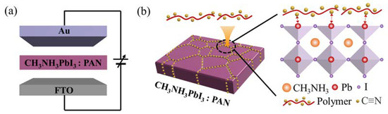
Figure 1.
(a) Schematic illustration of an Au/CH3NH3PbI3/FTO memristor device. (b) Schematic illustration of the PAN-passivated CH3NH3PbI3 films.
In order to investigate the correlation between the PAN additives’ concentration and grain size of the CH3NH3PbI3 perovskite films, we obtained the surface morphology SEM image of CH3NH3PbI3 perovskite films with 0–4 mg/mL of PAN additives’ concentration. Figure 2a–e illustrates the top-view SEM images of the CH3NH3PbI3 films with different concentrations of PAN (0 mg/mL (Control), 1 mg/mL (PAN-1), 2 mg/mL (PAN-2), 3 mg/mL (PAN-3), and 4 mg/mL (PAN-4), respectively). The CH3NH3PbI3 films exhibited larger grain size after PAN passivation compared to the control films without PAN passivation. With a modest concentration of PAN additives (1–3 mg/mL), the mean grain size of the CH3NH3PbI3 films increased from ~0.54 μm (PAN-1) and ~0.62 μm (PAN-2) to ~1.08 μm (PAN-3). We attribute the larger grain size to the PAN additives, which can provide nucleation sites to guide the preferential orientation growth of crystals and thereby increases the grain size [22,23]. It is worth noting that the sample PAN-3 presented the largest grain size (Figure 2d), which means that PAN-3 had the minimum number of GBs. To confirm the reproducibility of this method, three samples with the same amounts of reagents (PAN-3) were prepared. The top-view SEM image and the distribution statistics of the grain size are shown in Figure S1. Sample 1, sample 2, and sample 3 exhibited similar morphology and grain size, confirming the reproducibility of this method. However, a higher concentration (4 mg/mL) of PAN additives provided a surplus of nucleation sites for CH3NH3PbI3 films, thereby, led to a decrease in grain size (~0.63 μm) (Figure 2e). Figure 2f shows the distribution of the grain size and statistics of mean grain size in the CH3NH3PbI3 films prepared with different concentrations of PAN additives, which further supports that the largest grain size of CH3NH3PbI3 films was achieved at the PAN additives’ concentration of 3 mg/mL.
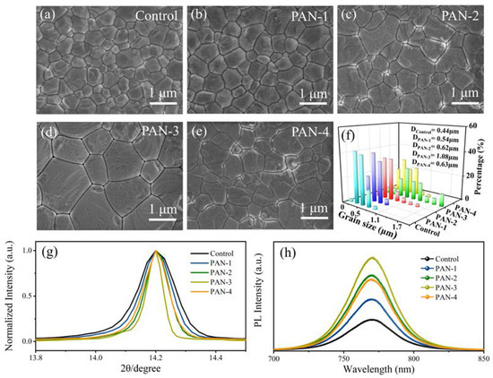
Figure 2.
Top-view SEM images of PAN passivation CH3NH3PbI3 films with different concentrations of PAN additives: (a) Control, (b) PAN-1, (c) PAN-2, (d) PAN-3, and (e) PAN-4. (f) Statistics of the averaged grain sizes of the CH3NH3PbI3 films under all the above conditions. (g) The normalized intensities of (110) diffraction peaks in the XRD patterns and (h) PL spectra of CH3NH3PbI3 films with different concentrations of PAN additives.
The effect of PAN additives on the crystallization of the CH3NH3PbI3 films was studied by XRD (Figure S2 and Figure 2g). XRD patterns of CH3NH3PbI3 films with different concentrations of PAN additives are shown in Figure S2. The XRD patterns of all CH3NH3PbI3 films samples revealed peaks at 14.2° and 28.5°, corresponding to the reflections from the (110) and (220) planes [24], respectively. The XRD patterns meant that the PAN additives had no effect on the crystal structure and orientation of CH3NH3PbI3. As shown in Figure 2g, by normalizing the (110) planes of the XRD patterns, the sample with the addition of PAN exhibited the narrower full-width at half-maximum, indicating the formation of larger grain size in the CH3NH3PbI3 film [25]. Moreover, we measured the PL spectra of the CH3NH3PbI3 films with different concentrations of PAN additives. Figure 2h reveals the tendency of PL intensity to remain fixed at ~765 nm for all the CH3NH3PbI3 film samples. We found that the PL intensities of the CH3NH3PbI3 films with PAN additives were higher than that of the control film, indicating that carrier recombination in the CH3NH3PbI3 layer was significantly inhibited, which means that the number of GBs of CH3NH3PbI3 films was reduced (GBs are the main nonradiative recombination centers) [26]. In addition, the UV–vis absorption spectra of the CH3NH3PbI3 films with different concentrations of PAN additives were also measured, as presented in Figure S3. When PAN concentration increased from 0 to 3 mg/mL, the light absorption intensities of the CH3NH3PbI3 films were enhanced slightly. By further increasing the PAN concentration, the light absorption intensity was reduced. The change in absorption would result from the combined effect of better crystallinity and increased grain size [27,28]. Based on the XRD, PL, and UV–vis absorption test results, it can be inferred that the PAN-3 sample exhibited the largest grain size, with a minimum number of GBs.
To study the effect of crystal grain size on the RS performance of the CH3NH3PbI3 memristor, the electrical characteristics of the memristor devices with different concentrations of PAN additives were systematically investigated (Figure 3). As shown in Figure 3(a-1)–(e-1), I–V characteristics curves of ten consecutive RS cycles in the memristor with five types of CH3NH3PbI3 films were measured, and the measurements were carried out under dark conditions. The voltage applied on the Au top electrode was swept by a DC bias voltage as follows: 0 V→1 V→0 V→−0.6 V→0 V, and the limiting current was set as 1 mA to prevent the hard breakdown of the device. The five types of CH3NH3PbI3 memristors presented the typical bipolar RS behaviors. When positive voltage was swept to a SET value (VSET), the resistance of the device was changed from the high-resistance state (HRS) to the low-resistance state (LRS). When negative voltage was swept to a RESET value (VRESET), the resistance state was switched from LRS to the HRS. In general, for a fresh CH3NH3PbI3 memristor device, the electroforming process is required to activate the subsequent RS behavior [29]. The high voltage used in the electroforming process can generate defects in the CH3NH3PbI3 layer. For the CH3NH3PbI3 materials, iodide ions are the main migration defect due to the low migration barrier [7]. However, the five types of CH3NH3PbI3 memristors prepared in this work did not require the electroforming process to activate, which may be due to the production of sufficient iodide defects during the CH3NH3PbI3 films’ deposition process.
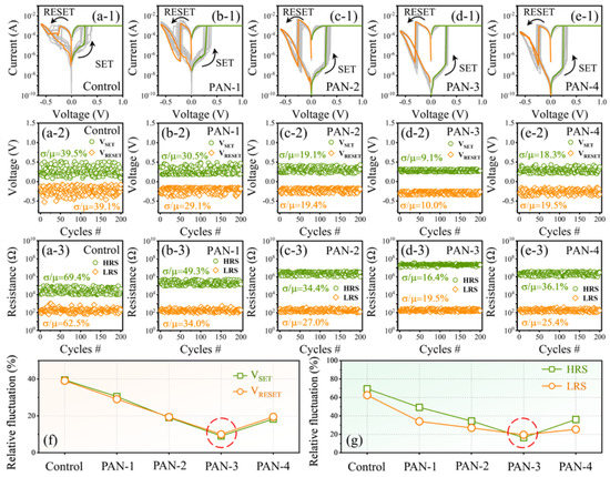
Figure 3.
RS performance of the Au/CH3NH3PbI3/FTO memristors with five different concentrations of PAN additives. (a-1–e-1) Typical I−V curves of the devices. Statistic (a-2–e-2) HRS/LRS and (a-3–e-3) VSET/VRESET of the memristor devices over 200 cycles. (f,g) The relative fluctuations in VSET/VRESET and HRS/LRS of the memristor devices.
Figure 3(a-2)–(e-2) and Figure 3(a-3)–(e-3) show the relative distributions of VSET/VRESET and HRS/LRS, respectively, in the five types CH3NH3PbI3 memristors for 200 consecutive RS cycles. In previous reports, the relative fluctuation defined by σ/µ (σ is the standard deviation, µ is the mean value) is generally used to evaluate the fluctuation of the RS parameter of the memristor [30]. Compared with the CH3NH3PbI3 memristor devices without the PAN additives, the RS parameter fluctuations in the memristors with the PAN additives were significantly reduced. When the concentration of PAN increased from 0 to 3 mg/mL, the relative fluctuations of HRS/LRS and VSET/VRESET were reduced from 69.4%/62.5% and 39.5%/39.1% to 16.4%/19.5% and 9.1%/10.0%, respectively. Further increasing the concentration of PAN additives to 4 mg/mL impeded the optimization of the relative fluctuations in RS parameters. The relative fluctuation coefficients of VSET/VRESET and HRS/LRS during 200 consecutive RS cycles in the five types of CH3NH3PbI3 memristors are more clearly demonstrated in Figure 3f,g. The relative fluctuation coefficients of VSET/VRESET and HRS/LRS show a similar variation trend to the number of GBs in CH3NH3PbI3 films (as shown in Figure 2a–e), first reducing and then increasing with the change in PAN concentration. To sum up, the PAN-3 memristor exhibits minimal RS parameter fluctuations, which could benefit from the reduction in the number of GBs in the CH3NH3PbI3 films.
Complex defects such as vacancies, interstitials, and anti-site occupations have been reported to exist in the solution-proceeding polycrystalline CH3NH3PbI3 films [31]. Among them, the iodide ions have a low activation energy and easily migrate under the action of electric field [7]. Thus, in previously reported studies of CH3NH3PbI3-based memristors, the RS mechanism is usually attributed to the formation and rupture of CFs resulting from iodide ions migration [10]. In addition, it has been reported that the activation energy of iodide ions’ migration at the GBs may be lower than that in the grain interior [32]. Based on the above reasons, it is reasonable to believe that the iodide vacancies-assisted CFs are mainly formed at GBs. Thus, the decrease in GBs can reduce the migration paths of iodide ions, a phenomenon which is responsible for the reduction in the randomness of CFs and the improved uniformity of RS parameters.
According to previous reports, the light can also induce the redistribution of iodide vacancies, and the recombination process of iodide vacancies and iodide ions in the film are then promoted [7]. As reported by Lu et al., light illumination can facilitate the breakage of CFs in the CH3NH3PbI3 films [7]. We studied the optoelectronic characteristics of the optimized PAN-3 memristor device during the RESET process using visible light with different intensities. Herein, the visible light is obtained with a xenon lamp source (the spectrum is shown in Figure 4a). The PAN-3 sample films shows the optical absorption in the visible light range (Figure 4a). As shown in Figure 4b, we can see that VRESET decreased significantly after visible light stimulation. The VRESET required to switch the memristor device steadily decreased from −0.31 V to −0.09 V when the light intensity was increased from 0 to 2 mW/cm2. We also studied the effect of light wavelengths on the RESET process of the optoelectronic memristor. Three different wavelengths, centered at 415 nm (blue light), 543 nm (green light), and 620 nm (red light), were obtained by applying different bandpass filters to the visible light source, and their spectra can be found in Figure S4a. It is interesting that the VRESET reduced from −0.31 V to 0.15 V, 0.19 V, and 0.24 V after the same intensity irradiation processes of blue light, green light, and red light (Figure S4b), respectively. We can find that the dependence tendency between VRESET and the light wavelength is consistent with the light absorption intensity of the PAN-3 sample films (Figure 4a), that is, the shorter wavelength light is more effective in reducing the VRESET; such a feather can be developed for distinguishing colors. On the other hand, further measurements showed that, after programming the optoelectronic memristors to LRS in the dark, high-intensity visible light irradiation (4–10 mW/cm2) can result in rapid failure of LRS retention (Figure 4c). In this case, the optoelectronic memristor can switch from the LRS to the HRS with light illumination. It is worth noting that the above results support the ability of applied electric field and light irradiation to control ion migration process in the CH3NH3PbI3 films, which can be utilized to realize photocoupled memristor devices. As shown in Figure 4d, reproductive switching can be achieved by alternating electrical and optical stimuli. The visible light intensity of 10 mW/cm2 was used in the subsequent electrical SET and optical RESET cycle tests. As shown in Figure 4d, the optimized PAN-3 memristor device was tested over 100 optoelectronic cycles, and the device showed good repeatability and non-volatile performance.
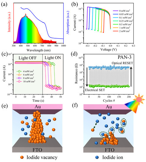
Figure 4.
(a) Absorption spectra of the CH3NH3PbI3 film (PAN-3) and the spectra of visible light source. (b) The RESET processes of the memristor device under different light intensities. (c) Evolution of LRS of the CH3NH3PbI3 memristor device under light irradiation. (d) Cyclic electrical SET and optical RESET of the CH3NH3PbI3 memristor device. Schematic diagrams of (e) the electrical SET and (f) the optical RESET mechanism.
The above results indicate that the iodide vacancies-assisted CFs may rupture when the memristor is stimulated by light. This supposition is also supported by previous research. Angelis et al. proposed a model in which light illumination induced the annihilation of iodide ion/iodide vacancy Frenkel pairs in the CH3NH3PbI3 films by combining experimental and theoretical studies [14]. Therefore, the RS mechanism of the CH3NH3PbI3 memristor device in the process of electrical SET and optical RESET can be explained by the following model. In the initial state, a small number of iodide ions or iodide vacancies defects are randomly present in CH3NH3PbI3 films. As the voltage is applied, the iodide ions migrate towards the top electrode under the action of electric field and form iodide vacancies-assisted CFs (Figure 4e). When the CH3NH3PbI3 memristor is stimulated by light, the recombination process of iodide vacancies and iodide ions in the film is enhanced, resulting in the breakdown of CFs (Figure 4f).
Based on the optoelectronic switching characteristics of the optimized PAN-3 memristor device, we construct an optoelectronic memristor array (5 × 5, Figure 5a) to demonstrate the non-volatile image storage and image Boolean logic function. Visible light illumination on the device was controlled by a specific mask (Figure 5b). In this part of the work, the HRS and LRS states were defined as logical “1” and logical “0”, respectively. The operation mode of the optoelectronic memristor array was “electrical erase, optical write”. The initial CH3NH3PbI3 memristor devices were all in HRS and were pre-switched to LRS by applying a voltage pulse (1 V, 0.1 s) prior to the write operation (Figure 5c,d). The stability of resistance state is crucial for the memristor device to perform logical operations. In order to more intuitively evaluate the RS uniformity of the optoelectronic memristor array, the color maps of HRS (after optical write) and LRS (after electrical erase) for devices are shown in Figure S5a,c. The corresponding histogram distributions results are summarized in Figure S5b,d, respectively. These show that all devices could operate normally and the resistance state was uniform. As shown in Figure 5e, light stimulus (10 mW/cm2, 4 s) was applied to the array with an “H”-type metal mask, and the image of “H” was written to achieve image storage. The “H” image was still visible after 104 s (Figure 5f), indicating non-volatile optoelectronic information storage.

Figure 5.
(a) SEM image of the 5 × 5 memristor device array. (b) Schematic diagram of the image written operation. (c) The initial and (d) erasing state of the memristor array. (e) The “H” image written and (f) the non-volatile “H” image storage. (g–i) Image Boolean logic operation of the memristor device array.
The optoelectronic switching characteristics also enable the devices to perform image logical operations. Boolean operation is a key logic algorithm widely used in image processing [33]. Through Boolean logic operation, “X”- and “Y”-shape images can be transformed into a new image “N”, and the operational rule can be categorized into intersection (N = X ∩ Y), union (N = X ∪ Y), and subtraction (N = X − Y) [34,35,36]:
Herein, image Boolean operations (intersection, union, and subtraction) were successfully implemented with the CH3NH3PbI3 memristor. All memristors were pre-switched to LRS by applying an electrical pulse (1 V, 0.1 s), and a read electrical pulse (0.1 V, 0.1 s) was applied after each logic operation. For the “intersection” operation, the implementation process was as shown in Figure 5g. The “X” image was input with optical pulse (2 mW/cm2, 4 s) as input and the “Y” image was input with electrical pulse (−0.1 V, 0.1 s). Only the memristor devices subjected to both optical stimuli and electrical stimuli could be switched from LRS to HRS. Therefore, “V”-shape output image could be obtained. For the “union” operation, the implementation process was as shown in Figure 5h. Images “X” and “Y” were input with optical pulses (10 mW/cm2, 4 s). All memristors subjected to optical stimuli could be switched from LRS to HRS. The implementation of “subtraction” operation was as shown in Figure 5i. First, the optical pulse (10 mW/cm2, 4 s) was used as the input of the “X” image. Then, the “Y” shaped electrical image was input with an electrical pulse (1 V, 0.1 s). Only the resistance state of the (X − Y)-shaped region was HRS, while the other regions were LRS, indicating that the “subtraction” operation of Boolean logic had been implemented. In this part, the stability of switching voltage is crucial for the device to perform logical operations. For example, if the optoelectronic memristor with large switching voltage fluctuation (Control, 0 mg/mL PAN) is used to implement the intersection logic operation, some memristor devices would not be switched as desired. As shown in Figure S6, under the combined stimulation of −0.1 V voltage and 2 mW/cm2 light, a portion of the optoelectronic memristor does not switch from LRS to HRS, and the logic operation cannot be performed successfully. Hence, the structure modification to improve the switching uniformity of the memristor is of great importance for optoelectronic image-processing.
The interaction of light with the memristor device allows the information stored in the memristor to be controlled remotely. In addition, light-driven manipulation of the memristor state can also realize more complex and higher-order logic operations. In this work, we used binary input values of light intensity and electric voltage to achieve image Boolean logic operations. In fact, perovskite optoelectronic memristors can also achieve continuous changing of resistance states by modulating the stimuli (voltage pulses) [37]. In the future, we can also regulate light and voltage and monitor the input–output relationship in a continuous way, implementing fuzzy logic operations based on multi-valued logic [38,39].
4. Conclusions
In summary, the PAN passivation method was introduced to reduce the number of GBs in CH3NH3PbI3 films and minimize the CF randomness. As a result, the fluctuations in RS parameters (HRS/LRS and VSET/VRESET) in the optoelectronic CH3NH3PbI3 memristor devices was significantly reduced. In addition, the CH3NH3PbI3 memristor could be modulated, not only by electrical signals, but also by optical pulses. The unique optoelectronic characteristics enabled the device to achieve image sensing and image Boolean logic operations. This work provides an effective method for developing high-performance CH3NH3PbI3 optoelectronic memristors.
Supplementary Materials
The following supporting information can be downloaded at: https://www.mdpi.com/article/10.3390/nano13152174/s1, Figure S1: (a–c) The SEM images of three CH3NH3PbI3 films prepared with a same PAN concentration (3 mg/mL). (d–f) The distribution statistics of the grain size of sample 1, sample 2 and sample 3. Figure S2: XRD patterns of the CH3NH3PbI3 films with different concentrations of PAN additives. Figure S3: The optical absorption spectra of the CH3NH3PbI3 films with different concentrations of PAN additives. Figure S4: (a) The spectra distribution of light obtained by applying different bandpass filters to the visible light source. (b) The switching curve of the device with different light wavelength and the density is fixed at 1 mW/cm2. Figure S5: (a,c) Color maps of HRS and LRS of optoelectronic memristor array. (b,d) Histogram distributions of HRS and LRS in 36 optoelectronic memristor. Figure S6: Boolean intersection operations performed with the optoelectronic memristor (Control, 0 mg/mL PAN).
Author Contributions
Conceptualization, X.Z. (Xiaoning Zhao) and Z.W.; validation, X.Z. (Xiaohan Zhang) and X.Z. (Xiaoning Zhao); writing—review and editing, data curation, X.Z. (Xiaohan Zhang) and X.Z. (Xiaoning Zhao); supervision, Z.W. and X.Z. (Xiaoning Zhao). All authors have read and agreed to the published version of the manuscript.
Funding
This work was supported financially by the fund from the Department of Science and Technology of Jilin Province (Grant Nos. 20210201062GX and 20210509045RQ).
Data Availability Statement
All data generated and analyzed during this study are included in this article.
Conflicts of Interest
The authors declare no conflict of interest.
References
- Tan, S.; Zhou, N.; Chen, Y.; Li, L.; Liu, G.; Liu, P.; Zhu, C.; Lu, J.; Sun, W.; Chen, Q.; et al. Effect of high dipole moment cation on layered 2D organic-inorganic halide perovskite solar cells. Adv. Energy Mater. 2019, 9, 1803024. [Google Scholar] [CrossRef]
- Wang, F.; Li, X.; Wang, H.; Gou, Y.; Yang, S.; Han, D.; Yang, L.; Fan, L.; Yang, J.; Rosei, F. Supramolecular bridging strategy enables high performance and stable organic-inorganic halide perovskite solar cells. Chem. Eng. J. 2022, 446, 137431. [Google Scholar] [CrossRef]
- Meng, X.; Ji, S.; Wang, Q.; Wang, X.; Bai, T.; Zhang, R.; Yang, B.; Li, Y.; Shao, Z.; Jiang, J.; et al. Organic-inorganic hybrid cuprous-based metal halides for warm white light-emitting diodes. Adv. Sci. 2022, 9, 2203596. [Google Scholar] [CrossRef] [PubMed]
- Yan, S.; Tian, W.; Chen, H.; Tang, K.; Lin, T.; Zhong, G.; Qiu, L.; Pan, X.; Wang, W. Synthesis of 0D manganese-based organic-inorganic hybrid perovskite and its application in lead-free red light-emitting diode. Adv. Funct. Mater. 2021, 31, 2100855. [Google Scholar] [CrossRef]
- Lee, J.; Lee, W.; Lee, J.; Baek, K.-Y.; Shin, J.; Kim, J.-K.; Kim, J.; Ahn, H.; Kang, K.; Lee, T. Tailored design-of-experiments approach for device performance prediction and optimization of flash-evaporated organic-inorganic halide perovskite-based photodetectors. Adv. Mater. Technol. 2021, 6, 2001131. [Google Scholar] [CrossRef]
- Ahmadi, M.; Wu, T.; Hu, B. A review on organic-inorganic halide perovskite photodetectors: Device engineering and fundamental physics. Adv. Mater. 2017, 29, 1605242. [Google Scholar] [CrossRef]
- Zhu, X.; Lee, J.; Lu, W.D. Iodine vacancy redistribution in organic-inorganic halide perovskite films and resistive switching effects. Adv. Mater. 2017, 29, 1700527. [Google Scholar] [CrossRef] [PubMed]
- Zhang, C.; Li, Y.; Ma, C.; Zhang, Q. Recent progress of organic-inorganic hybrid perovskites in rram, artificial synapse, and logic operation. Small Sci. 2022, 2, 2100086. [Google Scholar] [CrossRef]
- Calado, P.; Telford, A.M.; Bryant, D.; Li, X.; Nelson, J.; O’Regan, B.C.; Barnes, P.R.F. Evidence for ion migration in hybrid perovskite solar cells with minimal hysteresis. Nat. Commun. 2016, 7, 13831. [Google Scholar] [CrossRef] [PubMed]
- Gu, C.; Lee, J.S. Flexible hybrid organic-inorganic perovskite memory. ACS Nano 2016, 10, 5413–5418. [Google Scholar] [CrossRef]
- Siddik, A.; Haldar, P.K.; Das, U.; Roy, A.; Sarkar, P.K. Organic-inorganic FAPbBr3 perovskite based flexible optoelectronic memory device for light-induced multi level resistive switching application. Mater. Chem. Phys. 2023, 297, 127292. [Google Scholar] [CrossRef]
- Xiao, X.; Hu, J.; Tang, S.; Yan, K.; Gao, B.; Chen, H.; Zou, D. Recent advances in halide perovskite memristors: Materials, structures, mechanisms, and applications. Adv. Mater. Technol. 2020, 5, 1900914. [Google Scholar] [CrossRef]
- DeQuilettes, D.W.; Zhang, W.; Burlakov, V.M.; Graham, D.J.; Leijtens, T.; Osherov, A.; Bulovi, V.; Snaith, H.J.; Ginger, D.S.; Stranks, S.D. Photo-induced halide redistribution in organic-inorganic perovskite films. Nat. Commun. 2016, 7, 11683. [Google Scholar] [CrossRef] [PubMed]
- Mosconi, E.; Meggiolaro, D.; Snaith, H.J.; Stranks, S.D.; Angelis, F.D. Light-induced annihilation of Frenkel defects in organo-lead halide perovskites. Energy Environ. Sci. 2016, 9, 3180–3187. [Google Scholar] [CrossRef]
- Yun, J.S.; Seidel, J.; Kim, J.; Soufiani, A.M.; Huang, S.; Lau, J.; Jeon, N.J.; Seok, S.I.; Green, M.A.; Ho-Baillie, A. Critical role of grain boundaries for ion migration in formamidinium and methylammonium lead halide perovskite solar cells. Adv. Energy Mater. 2016, 6, 1600330. [Google Scholar] [CrossRef]
- Lee, J.W.; Bae, S.H.; De Marco, N.; Hsieh, Y.-T.; Dai, Z.; Yang, Y. The role of grain boundaries in perovskite solar cells. Mater. Today Energy 2018, 7, 149–160. [Google Scholar] [CrossRef]
- Zhou, Y.; Yew, K.S.; Ang, D.S.; Kawashima, T.; Bera, M.K.; Zhang, H.Z.; Bersuker, G. White-light-induced disruption of nanoscale conducting filament in hafnia. Appl. Phys. Lett. 2015, 107, 072107. [Google Scholar] [CrossRef]
- Park, J.; Lee, S.; Yong, K. Photo-stimulated resistive switching of ZnO nanorods. Nanotechnology 2012, 23, 385707. [Google Scholar] [CrossRef] [PubMed]
- Liu, Z.; Cheng, P.; Li, Y.; Kang, R.; Zhang, Z.; Zuo, Z.; Zhao, J. High temperature CsPbBrxI3−x memristors based on hybrid electrical and optical resistive switching effects. ACS Appl. Mater. Interfaces 2021, 13, 58885–58897. [Google Scholar] [CrossRef]
- Zhou, F.; Liu, Y.; Shen, X.; Wang, M.; Yuan, F.; Chai, Y. Low-voltage, optoelectronic CH3NH3PbI3−xClx memory with integrated sensing and logic operations. Adv. Funct. Mater. 2018, 28, 1800080. [Google Scholar] [CrossRef]
- Ma, Y.; Zhang, H.; Zhang, Y.; Hu, R.; Jiang, M.; Zhang, R.; Lv, H.; Tian, J.; Chu, L.; Zhang, J.; et al. Enhancing the performance of inverted perovskite solar cells via grain boundary passivation with carbon quantum dots. ACS Appl. Mater. Interfaces 2018, 11, 3044–3052. [Google Scholar] [CrossRef] [PubMed]
- Chen, C.; Wang, X.; Li, Z.; Du, X.; Shao, Z.; Sun, X.; Liu, D.; Gao, C.; Hao, L.; Zhao, Q.; et al. Polyacrylonitrile-coordinated perovskite solar cell with open-circuit voltage exceeding 1.23 V. Angew. Chem. 2022, 134, e202113932. [Google Scholar]
- Zheng, Z.; Xia, M.; Chen, X.; Xiao, X.; Gong, J.; Liu, J.; Du, J.; Tao, Y.; Hu, Y.; Mei, A.; et al. Enhancing the performance of FA-based printable mesoscopic perovskite solar cells via the polymer additive. Adv. Energy Mater. 2023, 13, 2204335. [Google Scholar] [CrossRef]
- Yang, N.; Li, T.; Zhang, P.P.; Chen, X.; Hu, X.; Zhang, W. An early cancer diagnosis platform based on micro-magnetic sensor array demonstrates ultra-high sensitivity. J. Nanomed. Nanotechnol. 2016, 7, 1000407. [Google Scholar] [CrossRef]
- Heo, J.H.; Shin, D.H.; Moon, S.H.; Lee, M.H.; Kim, D.H.; Oh, S.H.; Jo, W.; Im, S.H. Memory effect behavior with respect to the crystal grain size in the organic-inorganic hybrid perovskite nonvolatile resistive random access memory. Sci. Rep. 2017, 7, 16586. [Google Scholar] [CrossRef]
- Chen, Q.; Ma, T.; Wang, F.; Liu, Y.; Liu, S.; Wang, J.; Cheng, Z.; Chang, Q.; Yang, R.; Huang, W.; et al. Rapid microwave-annealing process of hybrid perovskites to eliminate miscellaneous phase for high performance photovoltaics. Adv. Sci. 2020, 7, 2000480. [Google Scholar] [CrossRef]
- Hou, X.; Huang, S.; Ou-Yang, W.; Pan, L.; Sun, Z.; Chen, X. Constructing efficient and stable perovskite solar cells via interconnecting perovskite grains. ACS Appl. Mater. Interfaces 2017, 9, 35200–35208. [Google Scholar] [CrossRef] [PubMed]
- Peng, Y.; Liu, X.; Zhang, H.; Zhou, R.; Luo, H.; Lei, Y.; Zou, W.; Ni, Y.; Li, H.; Wang, H. Trap state passivation by barbital additive toward efficient perovskite solar cells with 22.65% efficiency. Energy Technol. 2022, 10, 2200354. [Google Scholar] [CrossRef]
- Ma, H.; Wang, W.; Xu, H.; Wang, Z.; Tao, Y.; Chen, P.; Liu, W.; Zhang, X.; Ma, J.; Liu, Y. Interface state-induced negative differential resistance observed in hybrid perovskite resistive switching memory. ACS Appl. Mater. Interfaces 2018, 10, 21755–21763. [Google Scholar] [CrossRef]
- Chen, L.; Xu, Y.; Sun, Q.Q.; Zhou, P.; Wang, P.F.; Ding, S.J.; Zhang, D.W. Atomic-layer-deposited HfLaO-based resistive switching memories with superior performance. IEEE Electron Device Lett. 2010, 31, 1296–1298. [Google Scholar] [CrossRef]
- Ball, J.M.; Petrozza, A. Defects in perovskite-halides and their effects in solar cells. Nat. Energy 2016, 1, 16149. [Google Scholar] [CrossRef]
- Yuan, Y.; Huang, J. Ion migration in organometal trihalide perovskite and its impact on photovoltaic efficiency and stability. Acc. Chem. Res. 2016, 49, 286–293. [Google Scholar] [CrossRef] [PubMed]
- Wang, X.; Gao, S. Image encryption algorithm based on the matrix semi-tensor product with a compound secret key produced by a Boolean network. Inform. Sci. 2020, 539, 195–214. [Google Scholar] [CrossRef]
- Shi, J.; Lin, Y.; Zeng, T.; Wang, Z.; Zhao, X.; Xu, H.; Liu, Y. Voltage-dependent plasticity and image Boolean operations realized in a WOx-based memristive synapse. J. Semicond. 2021, 42, 014102. [Google Scholar] [CrossRef]
- Mäntylä, M. Boolean operations of 2-manifolds through vertex neighborhood classification. ACM Trans. Graph. 1986, 5, 1–29. [Google Scholar] [CrossRef]
- Gardan, Y.; Perrin, E. An algorithm reducing 3D Boolean operations to a 2D problem: Concepts and results. Comput. Aid. Des. 1996, 28, 277–287. [Google Scholar] [CrossRef]
- Ma, F.; Zhu, Y.; Xu, Z.; Liu, Y.; Zheng, X.; Ju, S.; Li, Q.; Ni, Z.; Hu, H.; Chai, Y.; et al. Optoelectronic perovskite synapses for neuromorphic computing. Adv. Funct. Mater. 2020, 30, 1908901. [Google Scholar] [CrossRef]
- Gentili, P.L. The fuzziness of a chromogenic spirooxazine. Dye. Pigment. 2014, 110, 235–248. [Google Scholar] [CrossRef]
- Sahoo, A.; Baitalik, S. Fuzzy logic, artificial neural network, and adaptive neuro-fuzzy inference methodology for soft computation and modeling of ion sensing data of a terpyridyl-imidazole based bifunctional receptor. Front. Chem. 2022, 10, 864363. [Google Scholar] [CrossRef]


Disclaimer/Publisher’s Note: The statements, opinions and data contained in all publications are solely those of the individual author(s) and contributor(s) and not of MDPI and/or the editor(s). MDPI and/or the editor(s) disclaim responsibility for any injury to people or property resulting from any ideas, methods, instructions or products referred to in the content. |
© 2023 by the authors. Licensee MDPI, Basel, Switzerland. This article is an open access article distributed under the terms and conditions of the Creative Commons Attribution (CC BY) license (https://creativecommons.org/licenses/by/4.0/).