
Recent Understanding in the Chemical Vapor Deposition of Multilayer Graphene: Controlling Uniformity, Thickness, and Stacking Configuration
Abstract
:1. Introduction
2. CVD of Multilayer Graphene by a Precipitation/Segregation Mechanism
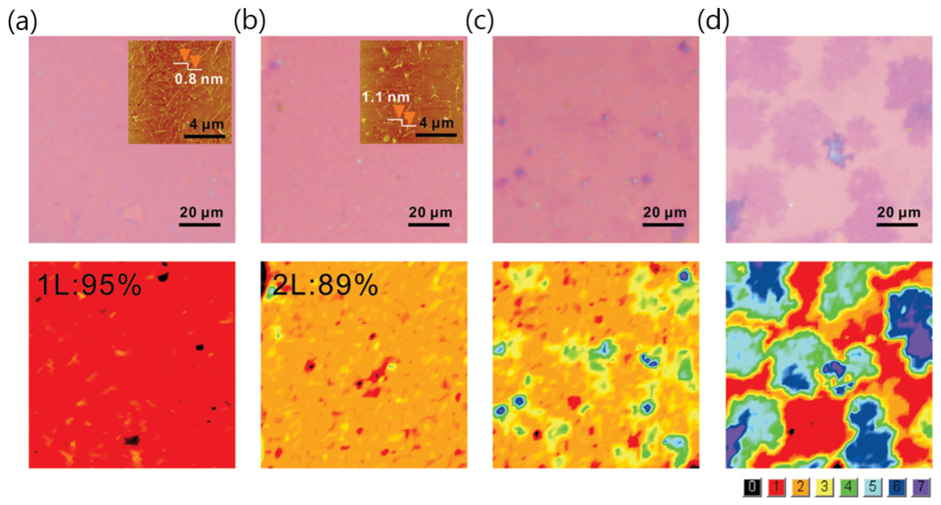
2.1. Ni Catalysts
2.2. Cu/Ni Alloys
3. CVD of Multilayer Graphene by Other Mechanisms
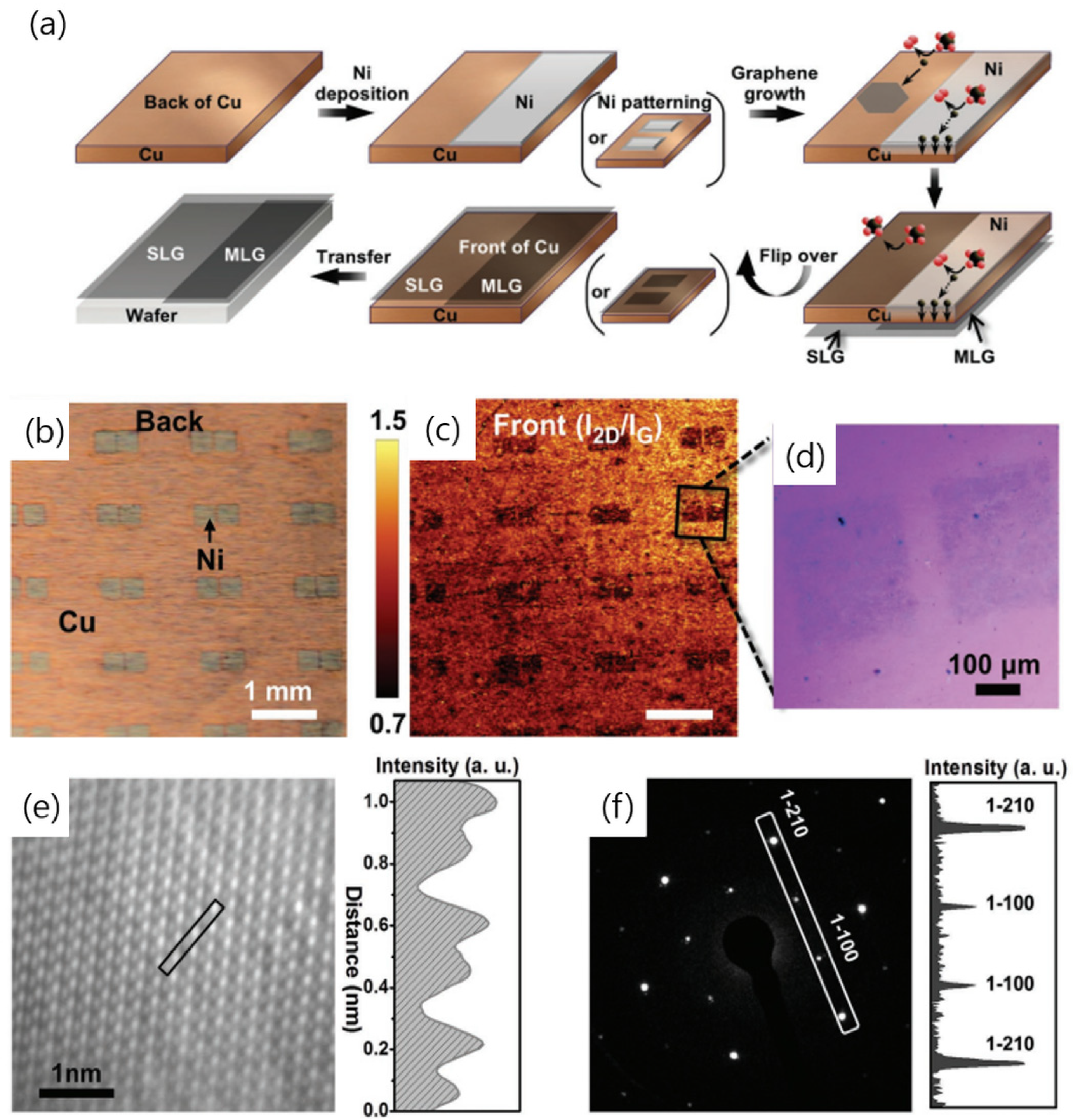
3.1. Bulk Diffusion of Carbon Atoms
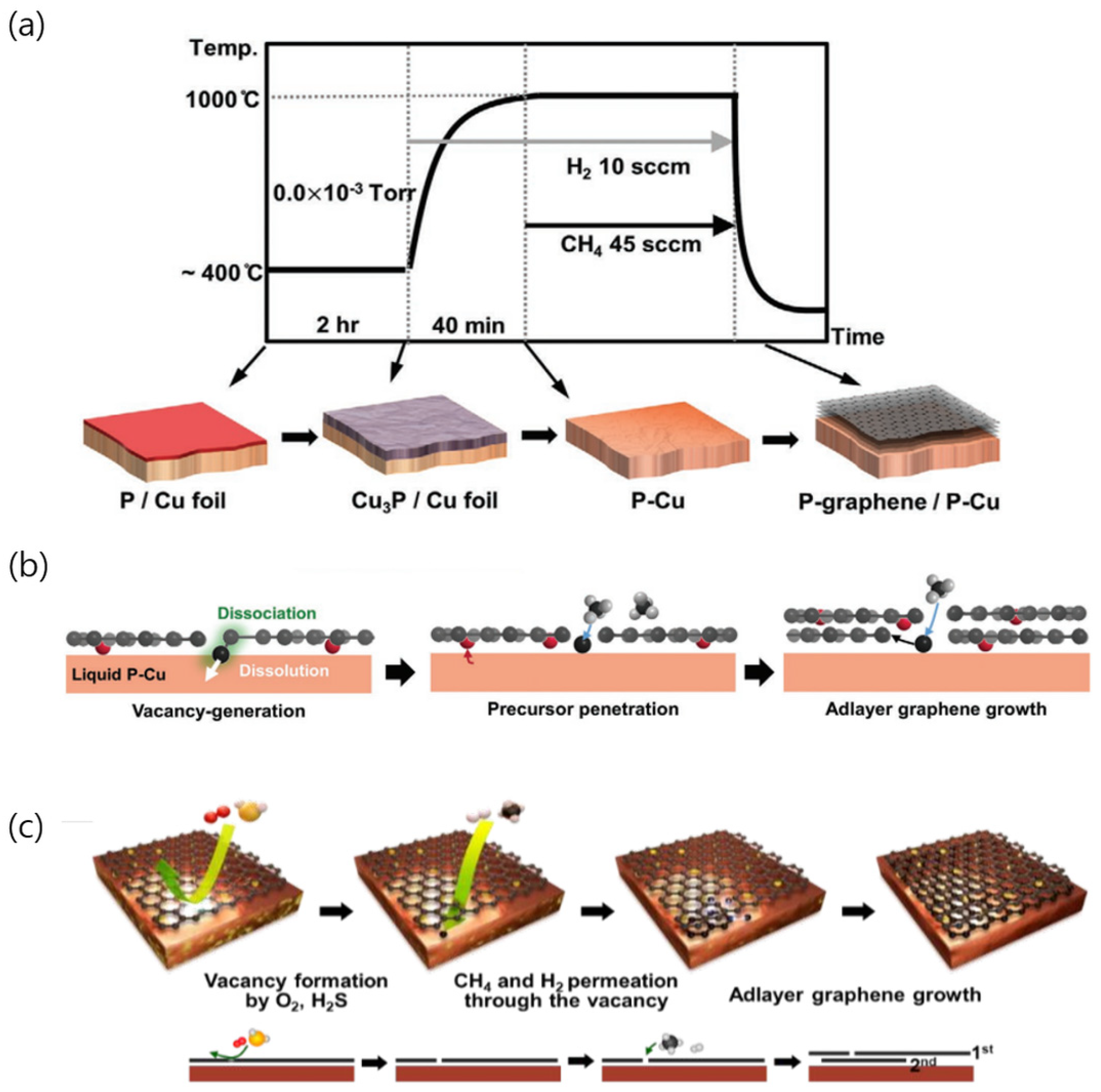
3.2. Intentional Formation of Vacancies in Graphene: Cu–P and Cu–S Alloys
4. Control of the Stacking Configuration of Bilayer Graphene
4.1. AB-Stacked Bilayer Graphene
4.1.1. Cu
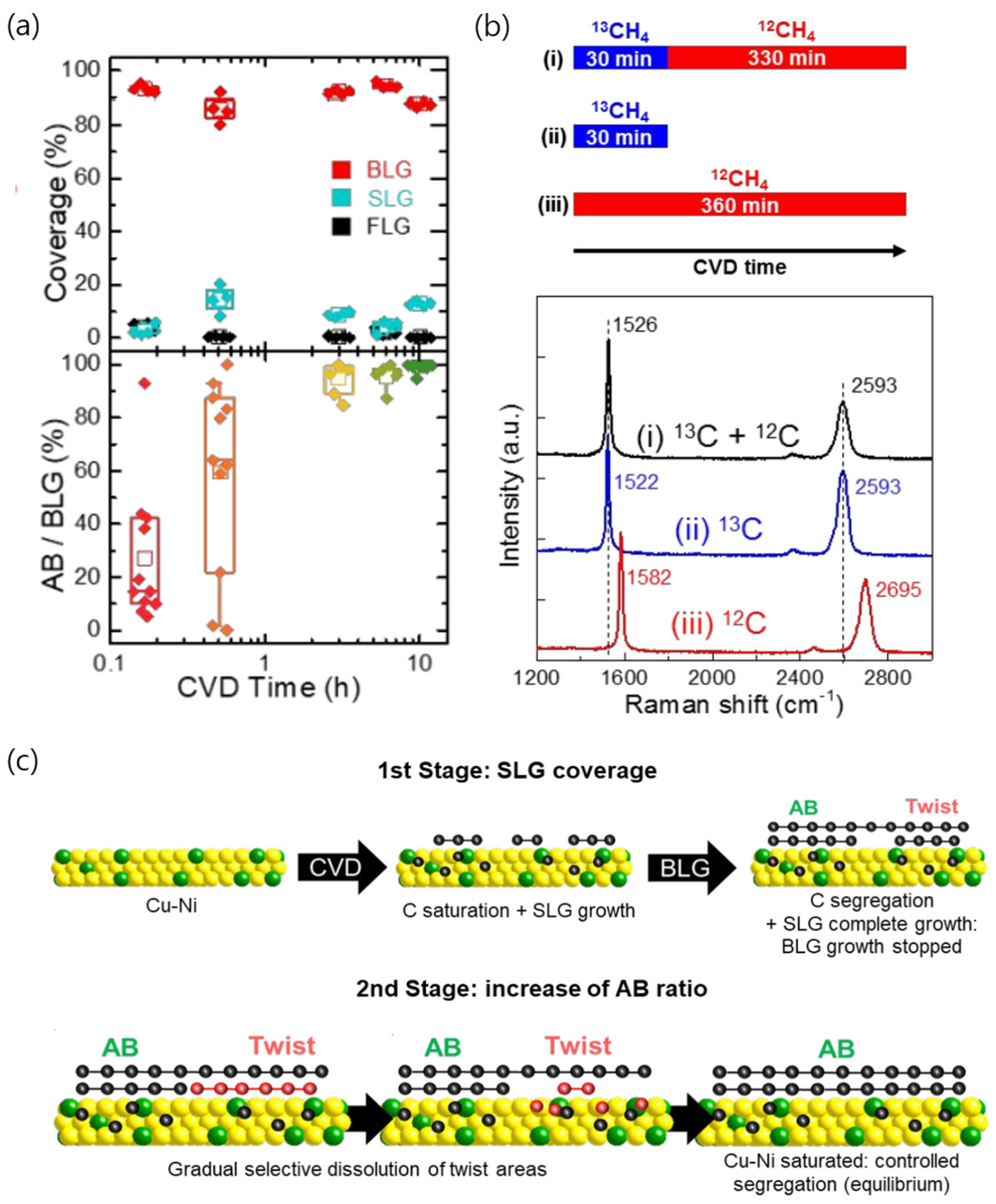
4.1.2. Cu/Ni Alloys
4.2. Twisted Bilayer Graphene
5. Summary and Perspectives
Supplementary Materials
Author Contributions
Funding
Data Availability Statement
Conflicts of Interest
References
- Novoselov, K.S.; Geim, A.K.; Morozov, S.V.; Jiang, D.-E.; Zhang, Y.; Dubonos, S.V.; Grigorieva, I.V.; Firsov, A.A. Electric field effect in atomically thin carbon films. Science 2004, 306, 666–669. [Google Scholar] [CrossRef] [Green Version]
- Zhang, Y.; Tan, Y.-W.; Stormer, H.L.; Kim, P. Experimental observation of the quantum Hall effect and Berry’s phase in graphene. Nature 2005, 438, 201–204. [Google Scholar] [CrossRef] [PubMed] [Green Version]
- Tombros, N.; Jozsa, C.; Popinciuc, M.; Jonkman, H.T.; Van Wees, B.J. Electronic spin transport and spin precession in single graphene layers at room temperature. Nature 2007, 448, 571–574. [Google Scholar] [CrossRef] [PubMed] [Green Version]
- Balandin, A.A.; Ghosh, S.; Bao, W.; Calizo, I.; Teweldebrhan, D.; Miao, F.; Lau, C.N. Superior thermal conductivity of single-layer graphene. Nano Lett. 2008, 8, 902–907. [Google Scholar] [CrossRef] [PubMed]
- Morozov, S.; Novoselov, K.; Katsnelson, M.; Schedin, F.; Elias, D.C.; Jaszczak, J.A.; Geim, A. Giant intrinsic carrier mobilities in graphene and its bilayer. Phys. Rev. Lett. 2008, 100, 016602. [Google Scholar] [CrossRef] [Green Version]
- Lin, Y.-M.; Dimitrakopoulos, C.; Jenkins, K.A.; Farmer, D.B.; Chiu, H.-Y.; Grill, A.; Avouris, P. 100-GHz transistors from wafer-scale epitaxial graphene. Science 2010, 327, 662. [Google Scholar] [CrossRef] [Green Version]
- Cao, L.; Meziani, M.J.; Sahu, S.; Sun, Y.-P. Photoluminescence properties of graphene versus other carbon nanomaterials. Acc. Chem. Res. 2013, 46, 171–180. [Google Scholar] [CrossRef]
- Naebe, M.; Wang, J.; Amini, A.; Khayyam, H.; Hameed, N.; Li, L.H.; Chen, Y.; Fox, B. Mechanical property and structure of covalent functionalised graphene/epoxy nanocomposites. Sci. Rep. 2014, 4, 4375. [Google Scholar] [CrossRef] [Green Version]
- Zhang, Y.; Tang, T.-T.; Girit, C.; Hao, Z.; Martin, M.C.; Zettl, A.; Crommie, M.F.; Shen, Y.R.; Wang, F. Direct observation of a widely tunable bandgap in bilayer graphene. Nature 2009, 459, 820–823. [Google Scholar] [CrossRef]
- Tang, T.-T.; Zhang, Y.; Park, C.-H.; Geng, B.; Girit, C.; Hao, Z.; Martin, M.C.; Zettl, A.; Crommie, M.F.; Louie, S.G. A tunable phonon–exciton Fano system in bilayer graphene. Nat. Nanotechnol. 2010, 5, 32–36. [Google Scholar] [CrossRef]
- Sharpe, A.L.; Fox, E.J.; Barnard, A.W.; Finney, J.; Watanabe, K.; Taniguchi, T.; Kastner, M.; Goldhaber-Gordon, D. Emergent ferromagnetism near three-quarters filling in twisted bilayer graphene. Science 2019, 365, 605–608. [Google Scholar] [CrossRef] [Green Version]
- Latil, S.; Meunier, V.; Henrard, L. Massless fermions in multilayer graphitic systems with misoriented layers: Ab initio calculations and experimental fingerprints. Phys. Rev. B 2007, 76, 201402. [Google Scholar] [CrossRef]
- Li, G.; Luican, A.; Lopes dos Santos, J.; Castro Neto, A.; Reina, A.; Kong, J.; Andrei, E. Observation of Van Hove singularities in twisted graphene layers. Nat. Phys. 2010, 6, 109–113. [Google Scholar] [CrossRef]
- Nam, N.N.; Koshino, M. Lattice relaxation and energy band modulation in twisted bilayer graphene. Phys. Rev. B 2017, 96, 075311. [Google Scholar] [CrossRef] [Green Version]
- Cao, Y.; Fatemi, V.; Demir, A.; Fang, S.; Tomarken, S.L.; Luo, J.Y.; Sanchez-Yamagishi, J.D.; Watanabe, K.; Taniguchi, T.; Kaxiras, E. Correlated insulator behaviour at half-filling in magic-angle graphene superlattices. Nature 2018, 556, 80–84. [Google Scholar] [CrossRef] [Green Version]
- Yankowitz, M.; Chen, S.; Polshyn, H.; Zhang, Y.; Watanabe, K.; Taniguchi, T.; Graf, D.; Young, A.F.; Dean, C.R. Tuning superconductivity in twisted bilayer graphene. Science 2019, 363, 1059–1064. [Google Scholar] [CrossRef] [Green Version]
- Cao, Y.; Fatemi, V.; Fang, S.; Watanabe, K.; Taniguchi, T.; Kaxiras, E.; Jarillo-Herrero, P. Unconventional superconductivity in magic-angle graphene superlattices. Nature 2018, 556, 43–50. [Google Scholar] [CrossRef] [Green Version]
- Codecido, E.; Wang, Q.; Koester, R.; Che, S.; Tian, H.; Lv, R.; Tran, S.; Watanabe, K.; Taniguchi, T.; Zhang, F. Correlated insulating and superconducting states in twisted bilayer graphene below the magic angle. Sci. Adv. 2019, 5, eaaw9770. [Google Scholar] [CrossRef] [Green Version]
- Reina, A.; Jia, X.; Ho, J.; Nezich, D.; Son, H.; Bulovic, V.; Dresselhaus, M.S.; Kong, J. Large area, few-layer graphene films on arbitrary substrates by chemical vapor deposition. Nano Lett. 2009, 9, 30–35. [Google Scholar] [CrossRef]
- Bae, S.; Kim, H.; Lee, Y.; Xu, X.; Park, J.-S.; Zheng, Y.; Balakrishnan, J.; Lei, T.; Ri Kim, H.; Song, Y.I. Roll-to-roll production of 30-inch graphene films for transparent electrodes. Nat. Nanotechnol. 2010, 5, 574–578. [Google Scholar] [CrossRef] [Green Version]
- Lee, S.; Lee, K.; Zhong, Z. Wafer scale homogeneous bilayer graphene films by chemical vapor deposition. Nano Lett. 2010, 10, 4702–4707. [Google Scholar] [CrossRef] [PubMed] [Green Version]
- Hao, Y.; Bharathi, M.; Wang, L.; Liu, Y.; Chen, H.; Nie, S.; Wang, X.; Chou, H.; Tan, C.; Fallahazad, B. The role of surface oxygen in the growth of large single-crystal graphene on copper. Science 2013, 342, 720–723. [Google Scholar] [CrossRef] [PubMed] [Green Version]
- Liu, W.; Kraemer, S.; Sarkar, D.; Li, H.; Ajayan, P.M.; Banerjee, K. Controllable and rapid synthesis of high-quality and large-area Bernal stacked bilayer graphene using chemical vapor deposition. Chem. Mater. 2014, 26, 907–915. [Google Scholar] [CrossRef]
- Wu, T.; Zhang, X.; Yuan, Q.; Xue, J.; Lu, G.; Liu, Z.; Wang, H.; Wang, H.; Ding, F.; Yu, Q. Fast growth of inch-sized single-crystalline graphene from a controlled single nucleus on Cu–Ni alloys. Nat. Mater. 2016, 15, 43–47. [Google Scholar] [CrossRef]
- Huang, M.; Biswal, M.; Park, H.J.; Jin, S.; Qu, D.; Hong, S.; Zhu, Z.; Qiu, L.; Luo, D.; Liu, X. Highly oriented monolayer graphene grown on a Cu/Ni (111) alloy foil. ACS Nano 2018, 12, 6117–6127. [Google Scholar] [CrossRef]
- Lin, L.; Peng, H.; Liu, Z. Synthesis challenges for graphene industry. Nat. Mater. 2019, 18, 520–524. [Google Scholar] [CrossRef]
- Huang, M.; Bakharev, P.V.; Wang, Z.-J.; Biswal, M.; Yang, Z.; Jin, S.; Wang, B.; Park, H.J.; Li, Y.; Qu, D. Large-area single-crystal AB-bilayer and ABA-trilayer graphene grown on a Cu/Ni (111) foil. Nat. Nanotechnol. 2020, 15, 289–295. [Google Scholar] [CrossRef]
- Li, X.; Cai, W.; An, J.; Kim, S.; Nah, J.; Yang, D.; Piner, R.; Velamakanni, A.; Jung, I.; Tutuc, E. Large-area synthesis of high-quality and uniform graphene films on copper foils. Science 2009, 324, 1312–1314. [Google Scholar] [CrossRef] [Green Version]
- Yan, K.; Peng, H.; Zhou, Y.; Li, H.; Liu, Z. Formation of bilayer bernal graphene: Layer-by-layer epitaxy via chemical vapor deposition. Nano Lett. 2011, 11, 1106–1110. [Google Scholar] [CrossRef]
- Liu, L.; Zhou, H.; Cheng, R.; Yu, W.J.; Liu, Y.; Chen, Y.; Shaw, J.; Zhong, X.; Huang, Y.; Duan, X. High-yield chemical vapor deposition growth of high-quality large-area AB-stacked bilayer graphene. ACS Nano 2012, 6, 8241–8249. [Google Scholar] [CrossRef] [Green Version]
- Sun, Z.; Raji, A.-R.O.; Zhu, Y.; Xiang, C.; Yan, Z.; Kittrell, C.; Samuel, E.; Tour, J.M. Large-area Bernal-stacked bi-, tri-, and tetralayer graphene. ACS Nano 2012, 6, 9790–9796. [Google Scholar] [CrossRef]
- Li, Q.; Chou, H.; Zhong, J.-H.; Liu, J.-Y.; Dolocan, A.; Zhang, J.; Zhou, Y.; Ruoff, R.S.; Chen, S.; Cai, W. Growth of adlayer graphene on Cu studied by carbon isotope labeling. Nano Lett. 2013, 13, 486–490. [Google Scholar] [CrossRef]
- Lu, C.-C.; Lin, Y.-C.; Liu, Z.; Yeh, C.-H.; Suenaga, K.; Chiu, P.-W. Twisting bilayer graphene superlattices. ACS Nano 2013, 7, 2587–2594. [Google Scholar] [CrossRef]
- Zhou, H.; Yu, W.J.; Liu, L.; Cheng, R.; Chen, Y.; Huang, X.; Liu, Y.; Wang, Y.; Huang, Y.; Duan, X. Chemical vapour deposition growth of large single crystals of monolayer and bilayer graphene. Nat. Commun. 2013, 4, 2096. [Google Scholar] [CrossRef] [Green Version]
- Fang, W.; Hsu, A.L.; Song, Y.; Birdwell, A.G.; Amani, M.; Dubey, M.; Dresselhaus, M.S.; Palacios, T.; Kong, J. Asymmetric growth of bilayer graphene on copper enclosures using low-pressure chemical vapor deposition. ACS Nano 2014, 8, 6491–6499. [Google Scholar] [CrossRef]
- Yan, Z.; Liu, Y.; Ju, L.; Peng, Z.; Lin, J.; Wang, G.; Zhou, H.; Xiang, C.; Samuel, E.; Kittrell, C. Large hexagonal bi-and trilayer graphene single crystals with varied interlayer rotations. Angew. Chem. 2014, 126, 1591–1595. [Google Scholar] [CrossRef]
- Hao, Y.; Wang, L.; Liu, Y.; Chen, H.; Wang, X.; Tan, C.; Nie, S.; Suk, J.W.; Jiang, T.; Liang, T. Oxygen-activated growth and bandgap tunability of large single-crystal bilayer graphene. Nat. Nanotechnol. 2016, 11, 426–431. [Google Scholar] [CrossRef] [Green Version]
- Ta, H.Q.; Perello, D.J.; Duong, D.L.; Han, G.H.; Gorantla, S.; Nguyen, V.L.; Bachmatiuk, A.; Rotkin, S.V.; Lee, Y.H.; Rümmeli, M.H. Stranski–Krastanov and Volmer–Weber CVD growth regimes to control the stacking order in bilayer graphene. Nano Lett. 2016, 16, 6403–6410. [Google Scholar] [CrossRef]
- Li, X.; Cai, W.; Colombo, L.; Ruoff, R.S. Evolution of graphene growth on Ni and Cu by carbon isotope labeling. Nano Lett. 2009, 9, 4268–4272. [Google Scholar] [CrossRef] [Green Version]
- Reina, A.; Thiele, S.; Jia, X.; Bhaviripudi, S.; Dresselhaus, M.S.; Schaefer, J.A.; Kong, J. Growth of large-area single-and Bi-layer graphene by controlled carbon precipitation on polycrystalline Ni surfaces. Nano Res. 2009, 2, 509–516. [Google Scholar] [CrossRef] [Green Version]
- Gong, Y.; Zhang, X.; Liu, G.; Wu, L.; Geng, X.; Long, M.; Cao, X.; Guo, Y.; Li, W.; Xu, J. Layer-controlled and wafer-scale synthesis of uniform and high-quality graphene films on a polycrystalline nickel catalyst. Adv. Funct. Mater. 2012, 22, 3153–3159. [Google Scholar] [CrossRef]
- Dahal, A.; Addou, R.; Sutter, P.; Batzill, M. Graphene monolayer rotation on Ni (111) facilitates bilayer graphene growth. Appl. Phys. Lett. 2012, 100, 241602. [Google Scholar] [CrossRef]
- Ahmed, M.; Kishi, N.; Sugita, R.; Fukaya, A.; Khatri, I.; Liang, J.; Mominuzzaman, S.M.; Soga, T.; Jimbo, T. Graphene synthesis by thermal chemical vapor deposition using solid precursor. J. Mater. Sci. Mater. 2013, 24, 2151–2155. [Google Scholar] [CrossRef]
- Kim, S.J.; Kim, D.W.; Jung, H.-T. Key growth parameters affecting the domain structure of chemical vapor deposition (CVD)-grown graphene on nickel. RSC Adv. 2013, 3, 22909–22913. [Google Scholar] [CrossRef]
- Tu, Z.; Liu, Z.; Li, Y.; Yang, F.; Zhang, L.; Zhao, Z.; Xu, C.; Wu, S.; Liu, H.; Yang, H. Controllable growth of 1–7 layers of graphene by chemical vapour deposition. Carbon 2014, 73, 252–258. [Google Scholar] [CrossRef] [Green Version]
- Lavin-Lopez, M.P.; Valverde, J.L.; Ruiz-Enrique, M.I.; Sanchez-Silva, L.; Romero, A. Thickness control of graphene deposited over polycrystalline nickel. New J. Chem. 2015, 39, 4414–4423. [Google Scholar] [CrossRef]
- Liu, X.; Fu, L.; Liu, N.; Gao, T.; Zhang, Y.; Liao, L.; Liu, Z. Segregation growth of graphene on Cu–Ni alloy for precise layer control. J. Phys. Chem. C 2011, 115, 11976–11982. [Google Scholar] [CrossRef]
- Liu, N.; Fu, L.; Dai, B.; Yan, K.; Liu, X.; Zhao, R.; Zhang, Y.; Liu, Z. Universal segregation growth approach to wafer-size graphene from non-noble metals. Nano Lett. 2011, 11, 297–303. [Google Scholar] [CrossRef]
- Zhang, Y.; Gomez, L.; Ishikawa, F.N.; Madaria, A.; Ryu, K.; Wang, C.; Badmaev, A.; Zhou, C. Comparison of graphene growth on single-crystalline and polycrystalline Ni by chemical vapor deposition. J. Phys. Chem. Lett. 2010, 1, 3101–3107. [Google Scholar] [CrossRef]
- Takesaki, Y.; Kawahara, K.; Hibino, H.; Okada, S.; Tsuji, M.; Ago, H. Highly uniform bilayer graphene on epitaxial Cu–Ni (111) alloy. Chem. Mater. 2016, 28, 4583–4592. [Google Scholar] [CrossRef]
- Jin, S.; Huang, M.; Kwon, Y.; Zhang, L.; Li, B.-W.; Oh, S.; Dong, J.; Luo, D.; Biswal, M.; Cunning, B.V. Colossal grain growth yields single-crystal metal foils by contact-free annealing. Science 2018, 362, 1021–1025. [Google Scholar] [CrossRef] [Green Version]
- Wang, H.; Yao, Z.; Jung, G.S.; Song, Q.; Hempel, M.; Palacios, T.; Chen, G.; Buehler, M.J.; Aspuru-Guzik, A.; Kong, J. Frank-van der Merwe growth in bilayer graphene. Matter 2021, 4, 3339–3353. [Google Scholar] [CrossRef]
- Yoo, M.S.; Lee, H.C.; Lee, S.; Lee, S.B.; Lee, N.S.; Cho, K. Chemical vapor deposition of bernal-stacked graphene on a Cu surface by breaking the carbon solubility symmetry in Cu foils. Adv. Mater. 2017, 29, 1700753. [Google Scholar] [CrossRef]
- Yoo, M.S.; Lee, H.C.; Lee, S.B.; Cho, K. Cu-Phosphorus Eutectic Solid Solution for Growth of Multilayer Graphene with Widely Tunable Doping. Adv. Funct. Mater. 2021, 31, 2006499. [Google Scholar] [CrossRef]
- Yoo, M.S.; Lee, H.C.; Wolf, C.; Nguyen, N.N.; Park, D.-H.; Kim, J.; Lee, E.; Chung, H.-J.; Cho, K. Growth of multilayer graphene with a built-in vertical electric field. Chem. Mater. 2020, 32, 5142–5152. [Google Scholar] [CrossRef]
- Solís-Fernández, P.; Terao, Y.; Kawahara, K.; Nishiyama, W.; Uwanno, T.; Lin, Y.-C.; Yamamoto, K.; Nakashima, H.; Nagashio, K.; Hibino, H. Isothermal growth and stacking evolution in highly uniform Bernal-stacked bilayer graphene. ACS Nano 2020, 14, 6834–6844. [Google Scholar] [CrossRef]
- Qi, Z.; Shi, H.; Zhao, M.; Jin, H.; Jin, S.; Kong, X.; Ruoff, R.S.; Qin, S.; Xue, J.; Ji, H. Chemical vapor deposition growth of bernal-stacked bilayer graphene by edge-selective etching with H2O. Chem. Mater. 2018, 30, 7852–7859. [Google Scholar] [CrossRef]
- Wei, W.; Zhang, C.; Li, H.; Pan, J.; Tan, Z.; Li, Y.; Cui, Y. In Situ Growth Dynamics of Uniform Bilayer Graphene with Different Twisted Angles Following Layer-by-Layer Mode. J. Phys. Chem. Lett. 2022, 13, 11201–11207. [Google Scholar] [CrossRef]
- Neto, A.C.; Guinea, F.; Peres, N.M.; Novoselov, K.S.; Geim, A.K. The electronic properties of graphene. Rev. Mod. Phys. 2009, 81, 109. [Google Scholar] [CrossRef] [Green Version]
- Uemura, K.; Ikuta, T.; Maehashi, K. Turbostratic stacked CVD graphene for high-performance devices. Jpn. J. Appl. Phys. 2018, 57, 030311. [Google Scholar] [CrossRef]
- Kim, M.; Kim, K.-J.; Lee, S.-J.; Kim, H.-M.; Cho, S.-Y.; Kim, M.-S.; Kim, S.-H.; Kim, K.-B. Highly stable and effective doping of graphene by selective atomic layer deposition of ruthenium. ACS Appl. Mater. 2017, 9, 701–709. [Google Scholar] [CrossRef] [PubMed]
- Piccinini, G.; Mišeikis, V.; Watanabe, K.; Taniguchi, T.; Coletti, C.; Pezzini, S. Parallel transport and layer-resolved thermodynamic measurements in twisted bilayer graphene. Phys. Rev. B 2021, 104, L241410. [Google Scholar] [CrossRef]
- Lim, H.; Lee, H.C.; Yoo, M.S.; Cho, A.; Nguyen, N.N.; Han, J.W.; Cho, K. Effects of hydrogen on the stacking orientation of bilayer graphene grown on copper. Chem. Mater. 2020, 32, 10357–10364. [Google Scholar] [CrossRef]
- Sun, L.; Wang, Z.; Wang, Y.; Zhao, L.; Li, Y.; Chen, B.; Huang, S.; Zhang, S.; Wang, W.; Pei, D. Hetero-site nucleation for growing twisted bilayer graphene with a wide range of twist angles. Nat. Commun. 2021, 12, 2391. [Google Scholar] [CrossRef]
- Cho, H.; Park, Y.; Kim, S.; Ahn, T.; Kim, T.-H.; Choi, H.C. Specific stacking angles of bilayer graphene grown on atomic-flat and-stepped Cu surfaces. NPJ 2D Mater. Appl. 2020, 4, 35. [Google Scholar] [CrossRef]


Disclaimer/Publisher’s Note: The statements, opinions and data contained in all publications are solely those of the individual author(s) and contributor(s) and not of MDPI and/or the editor(s). MDPI and/or the editor(s) disclaim responsibility for any injury to people or property resulting from any ideas, methods, instructions or products referred to in the content. |
© 2023 by the authors. Licensee MDPI, Basel, Switzerland. This article is an open access article distributed under the terms and conditions of the Creative Commons Attribution (CC BY) license (https://creativecommons.org/licenses/by/4.0/).
Share and Cite
Hong, H.C.; Ryu, J.I.; Lee, H.C. Recent Understanding in the Chemical Vapor Deposition of Multilayer Graphene: Controlling Uniformity, Thickness, and Stacking Configuration. Nanomaterials 2023, 13, 2217. https://doi.org/10.3390/nano13152217
Hong HC, Ryu JI, Lee HC. Recent Understanding in the Chemical Vapor Deposition of Multilayer Graphene: Controlling Uniformity, Thickness, and Stacking Configuration. Nanomaterials. 2023; 13(15):2217. https://doi.org/10.3390/nano13152217
Chicago/Turabian StyleHong, Hyo Chan, Jeong In Ryu, and Hyo Chan Lee. 2023. "Recent Understanding in the Chemical Vapor Deposition of Multilayer Graphene: Controlling Uniformity, Thickness, and Stacking Configuration" Nanomaterials 13, no. 15: 2217. https://doi.org/10.3390/nano13152217