Room Temperature Polymorphism in WO3 Produced by Resistive Heating of W Wires
Abstract
:1. Introduction
2. Materials and Methods
3. Results and Discussion
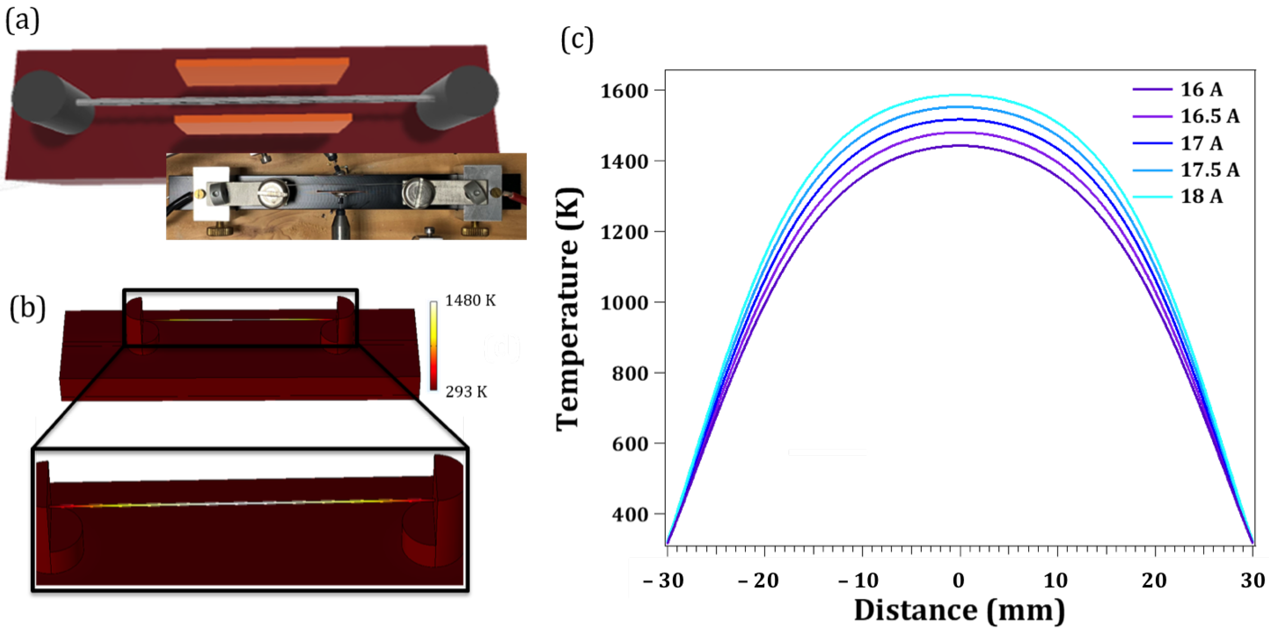
3.1. Synthesis Method
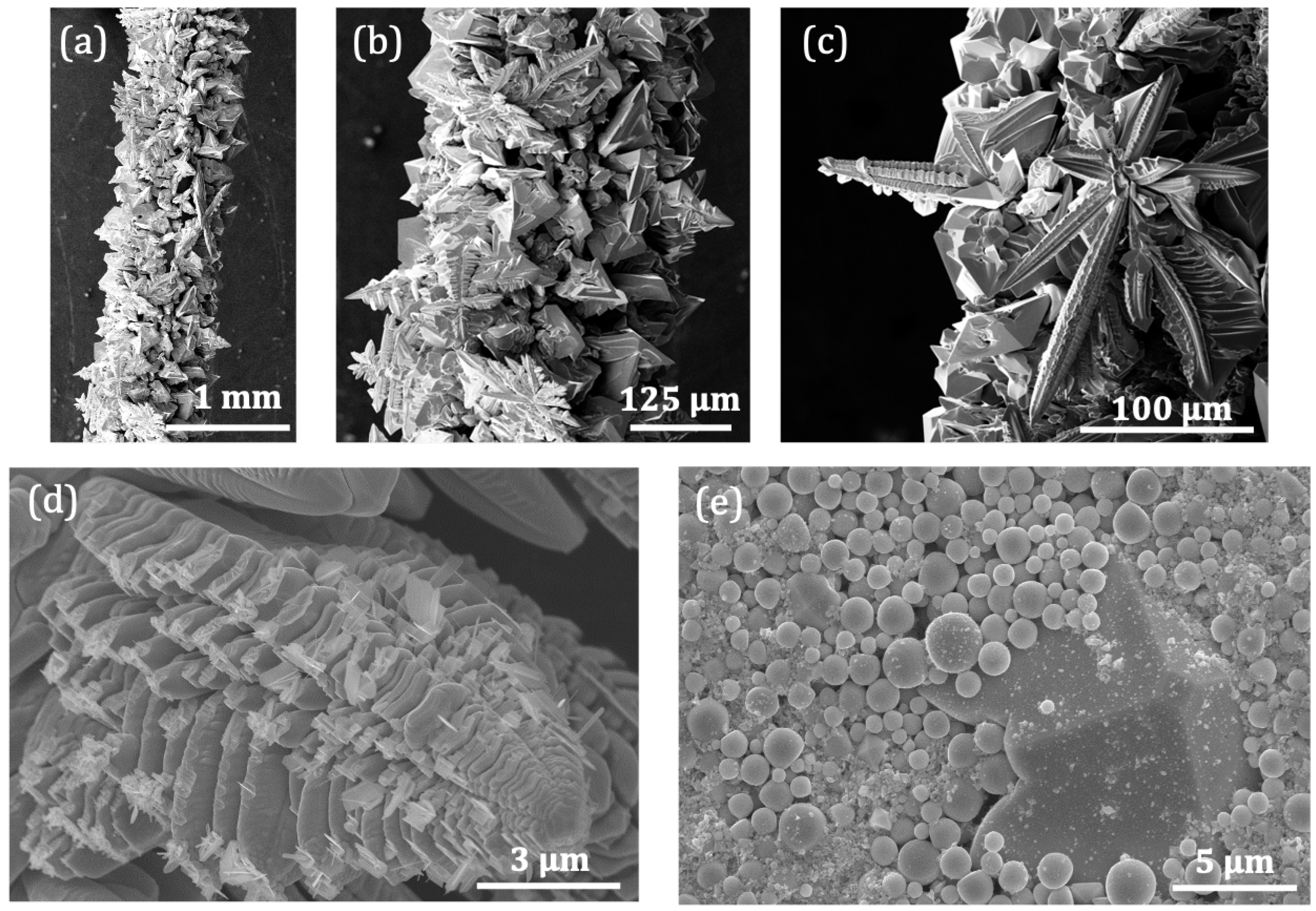
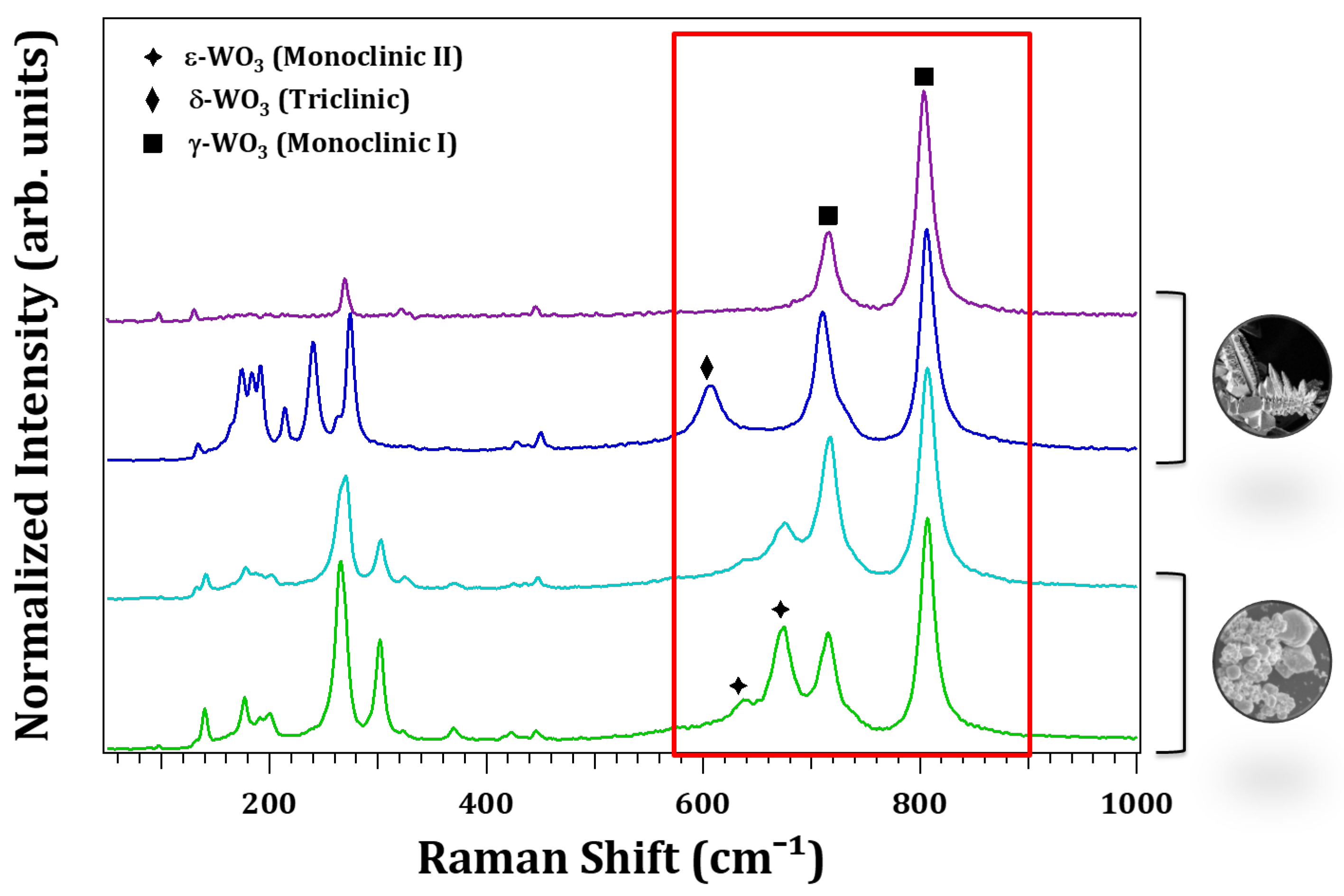
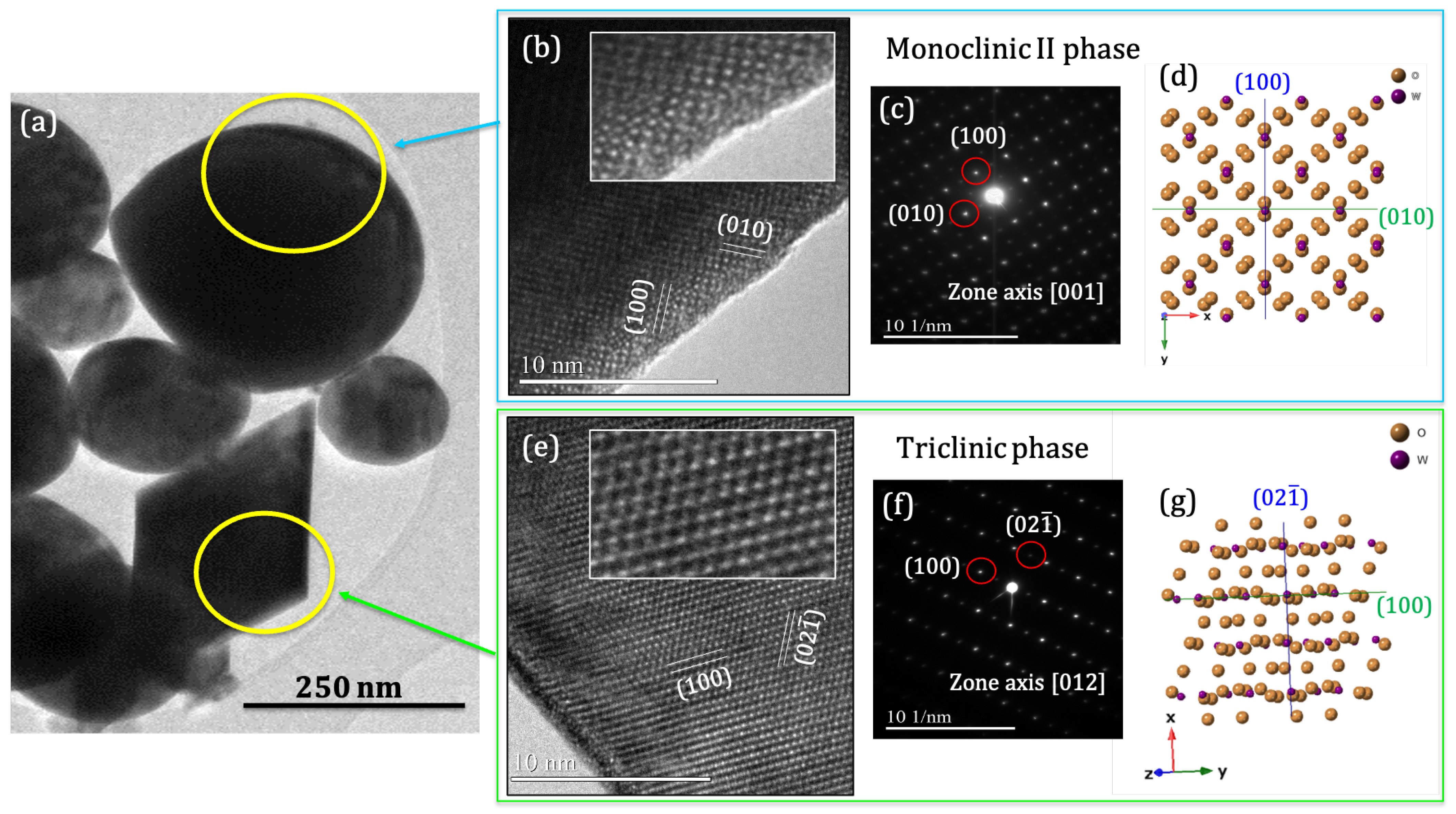
3.2. Structural Characterization
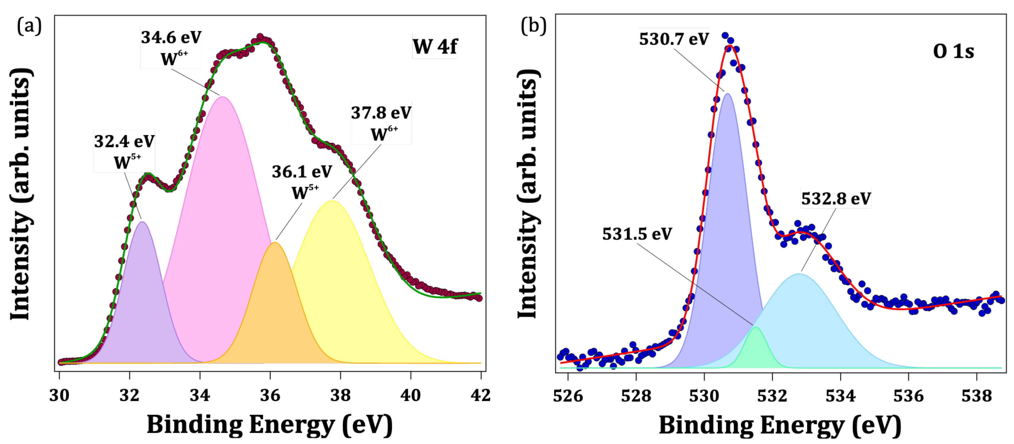
3.3. X-ray Photoelectron Spectroscopy (XPS) Study
4. Conclusions
Author Contributions
Funding
Data Availability Statement
Acknowledgments
Conflicts of Interest
References
- Zheng, H.; Ou, J.Z.; Strano, M.S.; Kaner, R.B.; Mitchell, A.; Kalantar-zadeh, K. Nanostructured Tungsten Oxide—Properties, Synthesis, and Applications. Adv. Funct. Mater. 2011, 21, 2175–2196. [Google Scholar] [CrossRef]
- Huang, Z.F.; Song, J.; Pan, L.; Zhang, X.; Wang, L.; Zou, J.J. Tungsten Oxides for Photocatalysis, Electrochemistry, and Phototherapy. Adv. Mater. 2015, 27, 5309–5327. [Google Scholar] [CrossRef] [PubMed]
- Salje, E.K.H.; Rehmann, S.; Pobell, F.; Morris, D.; Knight, K.S.; Herrmannsdörfer, T.; Dove, M.T. Crystal structure and paramagnetic behaviour of ϵ–WO3. J. Phys. Condens. Matter 1997, 9, 6563. [Google Scholar] [CrossRef]
- Cazzanelli, E.; Vinegoni, C.; Mariotto, G.; Kuzmin, A.; Purans, J. Low-Temperature Polymorphism in Tungsten Trioxide Powders and Its Dependence on Mechanical Treatments. J. Solid State Chem. 1999, 143, 24–32. [Google Scholar] [CrossRef] [Green Version]
- Filho, A.G.S.; Filho, J.M.; Freire, V.N.; Ayala, A.P.; Sasaki, J.M.; Freire, P.T.C.; Melo, F.E.A.; Julião, J.F.; Gomes, U.U. Phase transition in WO3 microcrystals obtained by sintering process. J. Raman Spectrosc. 2001, 32, 695–699. [Google Scholar] [CrossRef]
- Wang, L.; Teleki, A.; Pratsinis, S.E.; Gouma, P.I. Ferroelectric WO3 Nanoparticles for Acetone Selective Detection. Chem. Mater. 2008, 20, 4794–4796. [Google Scholar] [CrossRef]
- Boulova, M.; Lucazeau, G. Crystallite Nanosize Effect on the Structural Transitions of WO3 Studied by Raman Spectroscopy. J. Solid State Chem. 2002, 167, 425–434. [Google Scholar] [CrossRef]
- Jiang, X.; Herricks, T.; Xia, Y. CuO Nanowires Can Be Synthesized by Heating Copper Substrates in Air. Nano Lett. 2002, 2, 1333–1338. [Google Scholar] [CrossRef]
- Rackauskas, S.; Nasibulin, A.G.; Jiang, H.; Tian, Y.; Kleshch, V.I.; Sainio, J.; Obraztsova, E.D.; Bokova, S.N.; Obraztsov, A.N.; Kauppinen, E.I. A novel method for metal oxide nanowire synthesis. Nanotechnology 2009, 20, 165603. [Google Scholar] [CrossRef]
- Urbieta, A.; Sánchez, V.; Fernández, P.; Piqueras, J. Fast growth of undoped and Sn- and Tb-doped ZnO nanowires by Joule heating of Zn. CrystEngComm 2018, 20, 4449–4454. [Google Scholar] [CrossRef]
- Piqueras, J.; Hidalgo, P. Growth of Metal Oxide Nanostructures by Thermal Oxidation of Metals Under Influence of External Electric Fields and Electric Current Flow. Phys. Status Solidi A 2021, 218, 2100323. [Google Scholar] [CrossRef]
- Mallet, A.F.; Cebriano, T.; Méndez, B.; Piqueras, J. Rapid Synthesis of Undoped and Er Doped MoO3 Layered Plates by Resistive Heating of Molybdenum: Structural and Optical Properties. Phys. Status Solidi A 2018, 215, 1800471. [Google Scholar] [CrossRef]
- Rodríguez, B.; Hidalgo, P.; Piqueras, J.; Méndez, B. Influence of an external electric field on the rapid synthesis of MoO3 micro- and nanostructures by Joule heating of Mo wires. RSC Adv. 2020, 10, 11892–11897. [Google Scholar] [CrossRef] [PubMed] [Green Version]
- Tan, G.L.; Tang, D.; Dastan, D.; Jafari, A.; Silva, J.P.; Yin, X.T. Effect of heat treatment on electrical and surface properties of tungsten oxide thin films grown by HFCVD technique. Mater. Sci. Semicond. Process. 2021, 122, 105506. [Google Scholar] [CrossRef]
- Nagato, K.; Kojima, Y.; Kasuya, K.; Moritani, H.; Hamaguchi, T.; Nakao, M. Local Synthesis of Tungsten Oxide Nanowires by Current Heating of Designed Micropatterned Wires. Appl. Phys. Express 2008, 1, 014005. [Google Scholar] [CrossRef]
- Lin, S.K.; Liu, Y.C.; Chiu, S.J.; Liu, Y.T.; Lee, H.Y. The electromigration effect revisited: Non-uniform local tensile stress-driven diffusion. Sci. Rep. 2017, 7, 3082. [Google Scholar] [CrossRef]
- Mansourian, A.; Paknejad, S.A.; Wen, Q.; Vizcay-Barrena, G.; Fleck, R.; Zayats, A.; Mannan, S. Tunable Ultra-high Aspect Ratio Nanorod Architectures grown on Porous Substrate via Electromigration. Sci. Rep. 2016, 6, 22272. [Google Scholar] [CrossRef] [Green Version]
- Ponchut, C.; Rigal, J.M.; Clément, J.; Papillon, E.; Homs, A.; Petitdemange, S. MAXIPIX, a fast readout photon-counting X-ray area detector for synchrotron applications. J. Instrum. 2011, 6, C01069. [Google Scholar] [CrossRef] [Green Version]
- Roobol, S.; Onderwaater, W.; Drnec, J.; Felici, R.; Frenken, J. BINoculars: Data reduction and analysis software for two-dimensional detectors in surface X-ray diffraction. J. Appl. Crystallogr. 2015, 48, 1324–1329. [Google Scholar] [CrossRef] [Green Version]
- Desai, P.D.; Chu, T.K.; James, H.M.; Ho, C.Y. Electrical Resistivity of Selected Elements. J. Phys. Chem. Ref. Data 1984, 13, 1069–1096. [Google Scholar] [CrossRef]
- Tolias, P. Analytical expressions for thermophysical properties of solid and liquid tungsten relevant for fusion applications. Nucl. Mater. Energy 2017, 13, 42–57. [Google Scholar] [CrossRef]
- White, G.K.; Collocott, S.J. Heat Capacity of Reference Materials: Cu and W. J. Phys. Chem. Ref. Data 1984, 13, 1251–1257. [Google Scholar] [CrossRef]
- Tu, K.N.; Liu, Y.; Li, M. Effect of Joule heating and current crowding on electromigration in mobile technology. Appl. Phys. Rev. 2017, 4, 011101. [Google Scholar] [CrossRef]
- Polaczek, A.; Pekala, M.; Obuszko, Z. Magnetic susceptibility and thermoelectric power of tungsten intermediary oxides. J. Phys. Condens. Matter 1994, 6, 7909–7919. [Google Scholar] [CrossRef]
- Shpak, A.; Korduban, A.; Medvedskij, M.; Kandyba, V. XPS studies of active elements surface of gas sensors based on WO3−x nanoparticles. J. Electron Spectrosc. Relat. Phenom. 2007, 156–158, 172–175. [Google Scholar] [CrossRef]
- Shard, A.G. Practical guides for x-ray photoelectron spectroscopy: Quantitative XPS. J. Vac. Sci. Technol. A 2020, 38, 041201. [Google Scholar] [CrossRef]
- Dupin, J.C.; Gonbeau, D.; Vinatier, P.; Levasseur, A. Systematic XPS studies of metal oxides, hydroxides and peroxides. Phys. Chem. Chem. Phys. 2000, 2, 1319–1324. [Google Scholar] [CrossRef]
- Mehmood, F.; Iqbal, J.; Jan, T.; Mansoor, Q. Structural, Raman and photoluminescence properties of Fe doped WO3 nanoplates with anti cancer and visible light driven photocatalytic activities. J. Alloys Compd. 2017, 728, 1329–1337. [Google Scholar] [CrossRef]


Disclaimer/Publisher’s Note: The statements, opinions and data contained in all publications are solely those of the individual author(s) and contributor(s) and not of MDPI and/or the editor(s). MDPI and/or the editor(s) disclaim responsibility for any injury to people or property resulting from any ideas, methods, instructions or products referred to in the content. |
© 2023 by the authors. Licensee MDPI, Basel, Switzerland. This article is an open access article distributed under the terms and conditions of the Creative Commons Attribution (CC BY) license (https://creativecommons.org/licenses/by/4.0/).
Share and Cite
Rodríguez, B.; Dolado, J.; López-Sánchez, J.; Hidalgo, P.; Méndez, B. Room Temperature Polymorphism in WO3 Produced by Resistive Heating of W Wires. Nanomaterials 2023, 13, 884. https://doi.org/10.3390/nano13050884
Rodríguez B, Dolado J, López-Sánchez J, Hidalgo P, Méndez B. Room Temperature Polymorphism in WO3 Produced by Resistive Heating of W Wires. Nanomaterials. 2023; 13(5):884. https://doi.org/10.3390/nano13050884
Chicago/Turabian StyleRodríguez, Beatriz, Jaime Dolado, Jesus López-Sánchez, Pedro Hidalgo, and Bianchi Méndez. 2023. "Room Temperature Polymorphism in WO3 Produced by Resistive Heating of W Wires" Nanomaterials 13, no. 5: 884. https://doi.org/10.3390/nano13050884
APA StyleRodríguez, B., Dolado, J., López-Sánchez, J., Hidalgo, P., & Méndez, B. (2023). Room Temperature Polymorphism in WO3 Produced by Resistive Heating of W Wires. Nanomaterials, 13(5), 884. https://doi.org/10.3390/nano13050884


