
Isotopic Tracer Study of Initiation of Porosity in Anodic Alumina Formed in Chromic Acid


Abstract
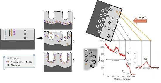
1. Introduction
2. Experimental
2.1. Specimen Preparation
- (a)
- First step: a constant current density of 3 mA/cm2 to 15 V in 0.4 mol/dm3 chromic acid at 313 K, prepared with water enriched in 18O to 10% (named electrolyte CR18).
- (b)
- Second step: a constant current density of 3 mA/cm2 for 30, 60, 120, and 300 s in 0.4 mol/dm3 chromic acid at 313 K, prepared with standard deionised water (named electrolyte CR16).
- (a)
- First step: a constant current density of 5 mA/cm2 to 20 V in 0.1 mol/dm3 sodium arsenate at 293 K, prepared with water enriched in 18O to 10% (named electrolyte AR18).
- (b)
- Second step: a constant current density of 3 mA/cm2 for 23, 120, and 300 s in 0.4 mol/dm3 chloric acid 313 K, prepared with standard deionised water (CR16).
2.2. Specimen Examination
3. Results and Discussion
3.1. Arsenic Species Mobility
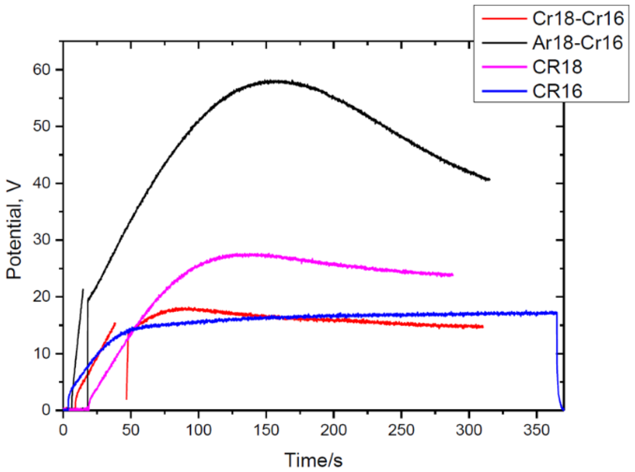
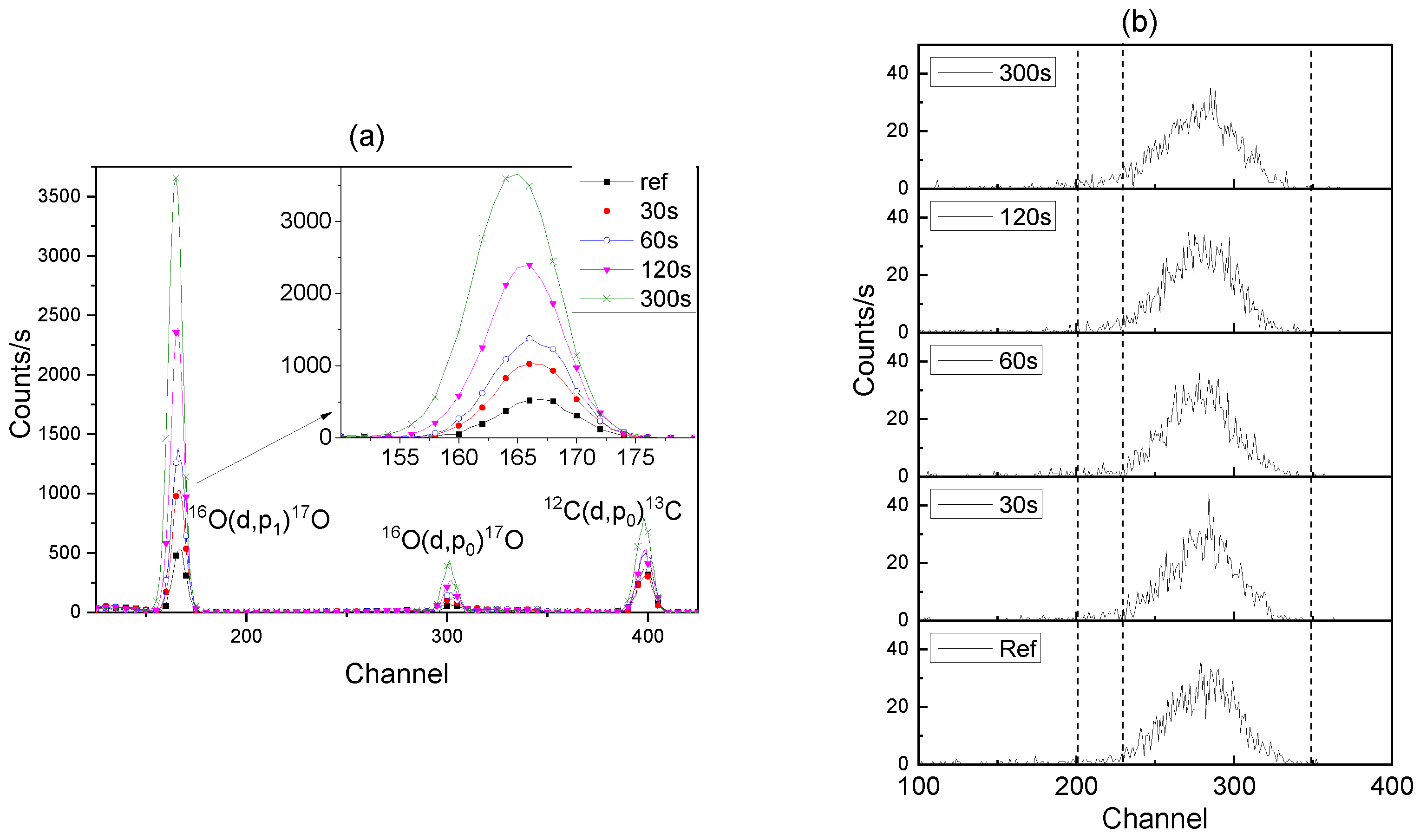
3.2. Formation of the Anodic Films—Voltage–Time Response
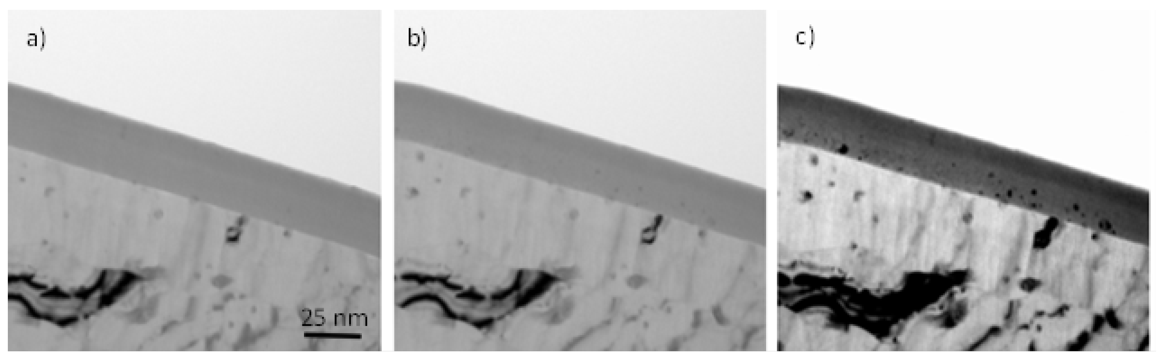
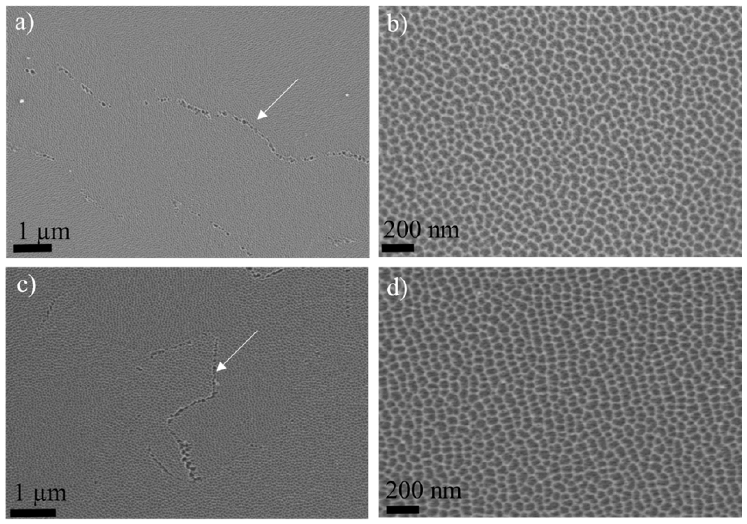
3.3. Substrate Morphology
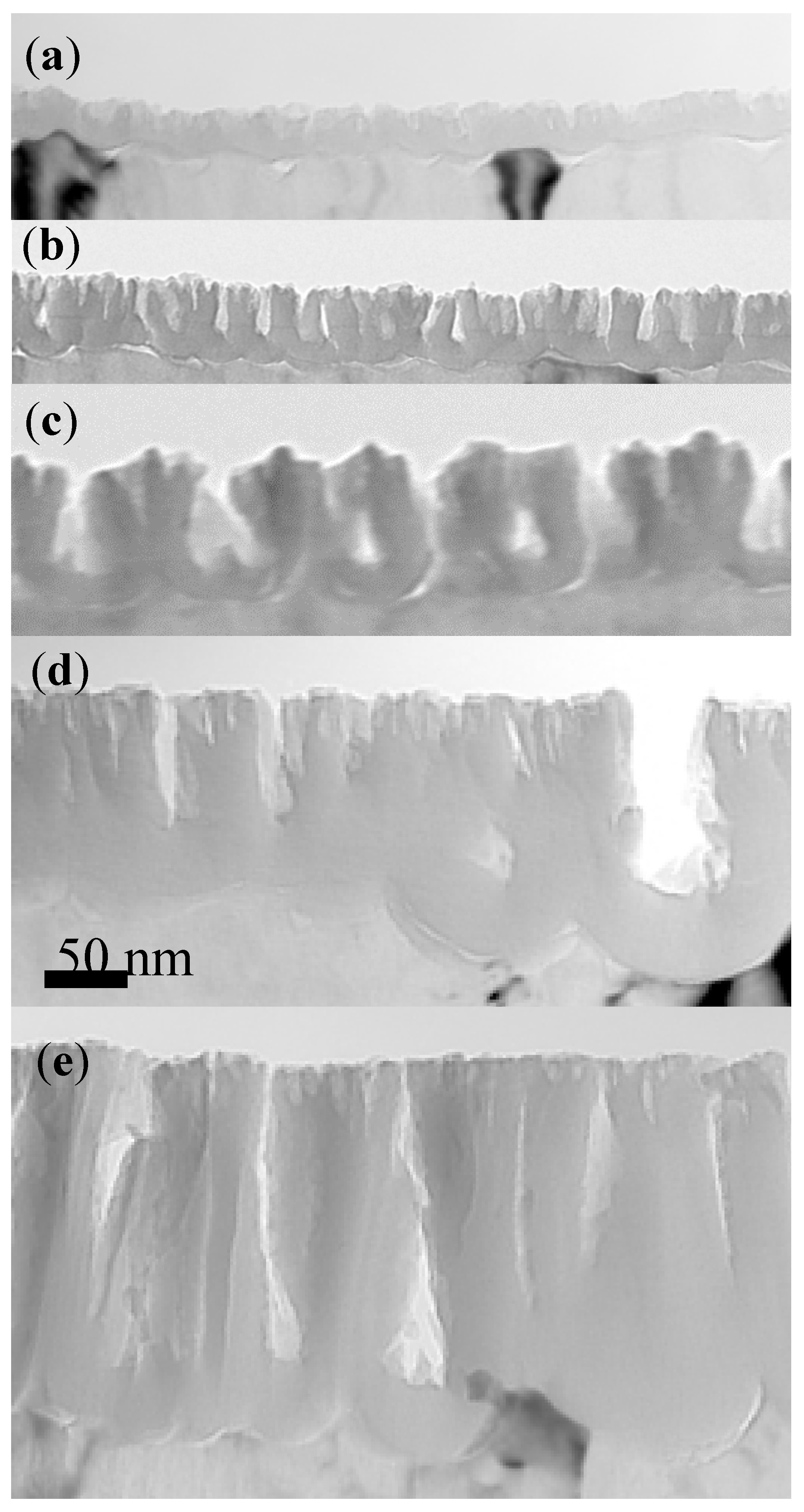
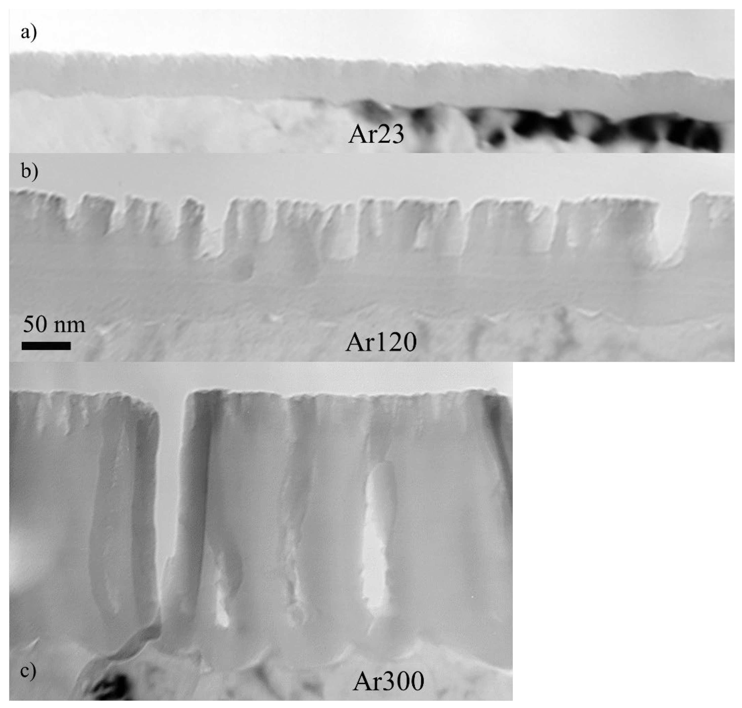
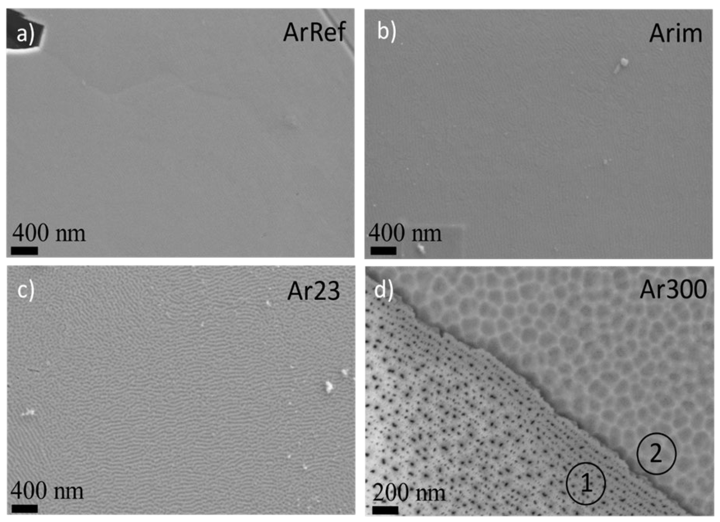
3.4. Re-Anodising in Chromic Acid—Film Morphology
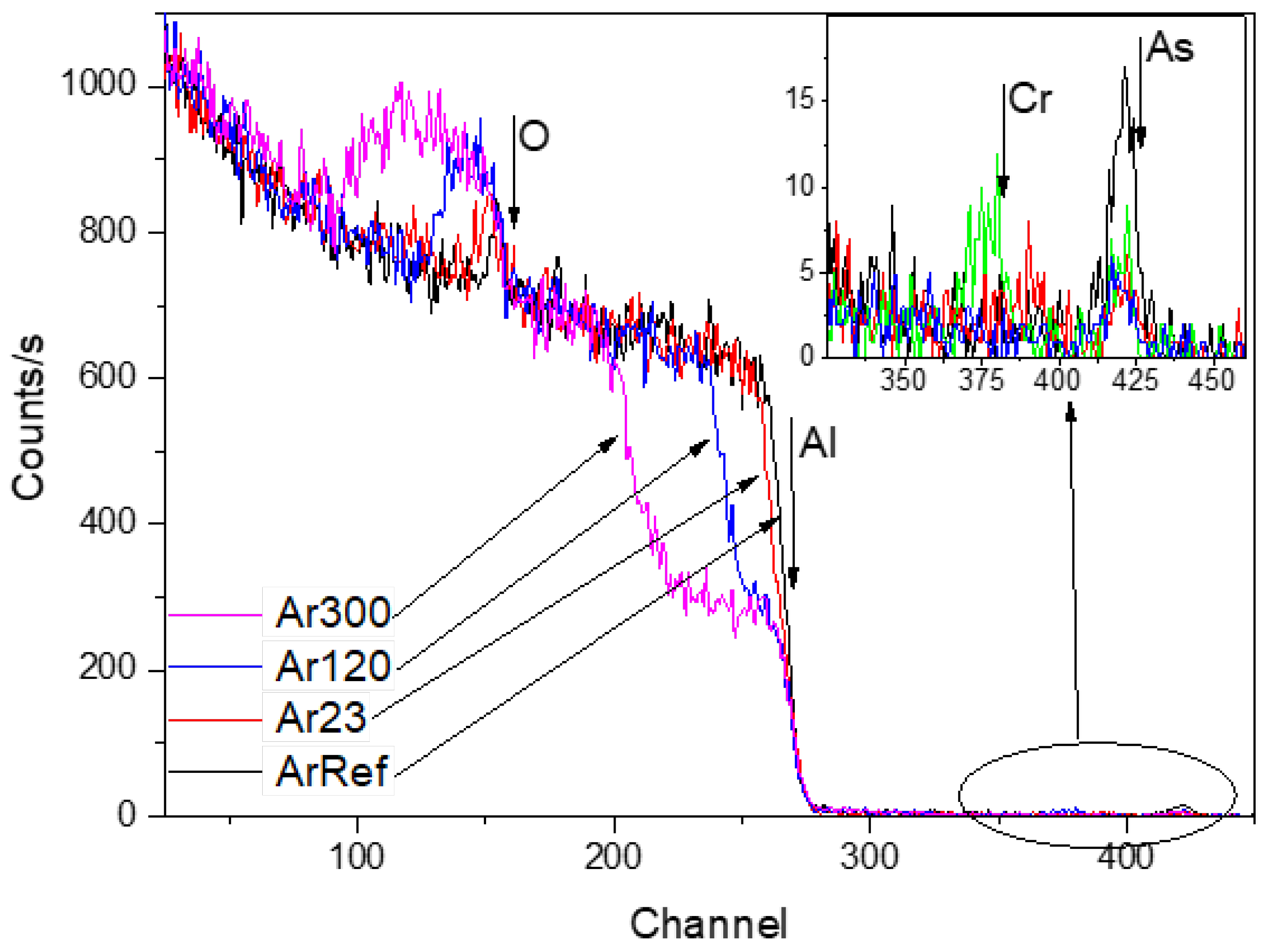
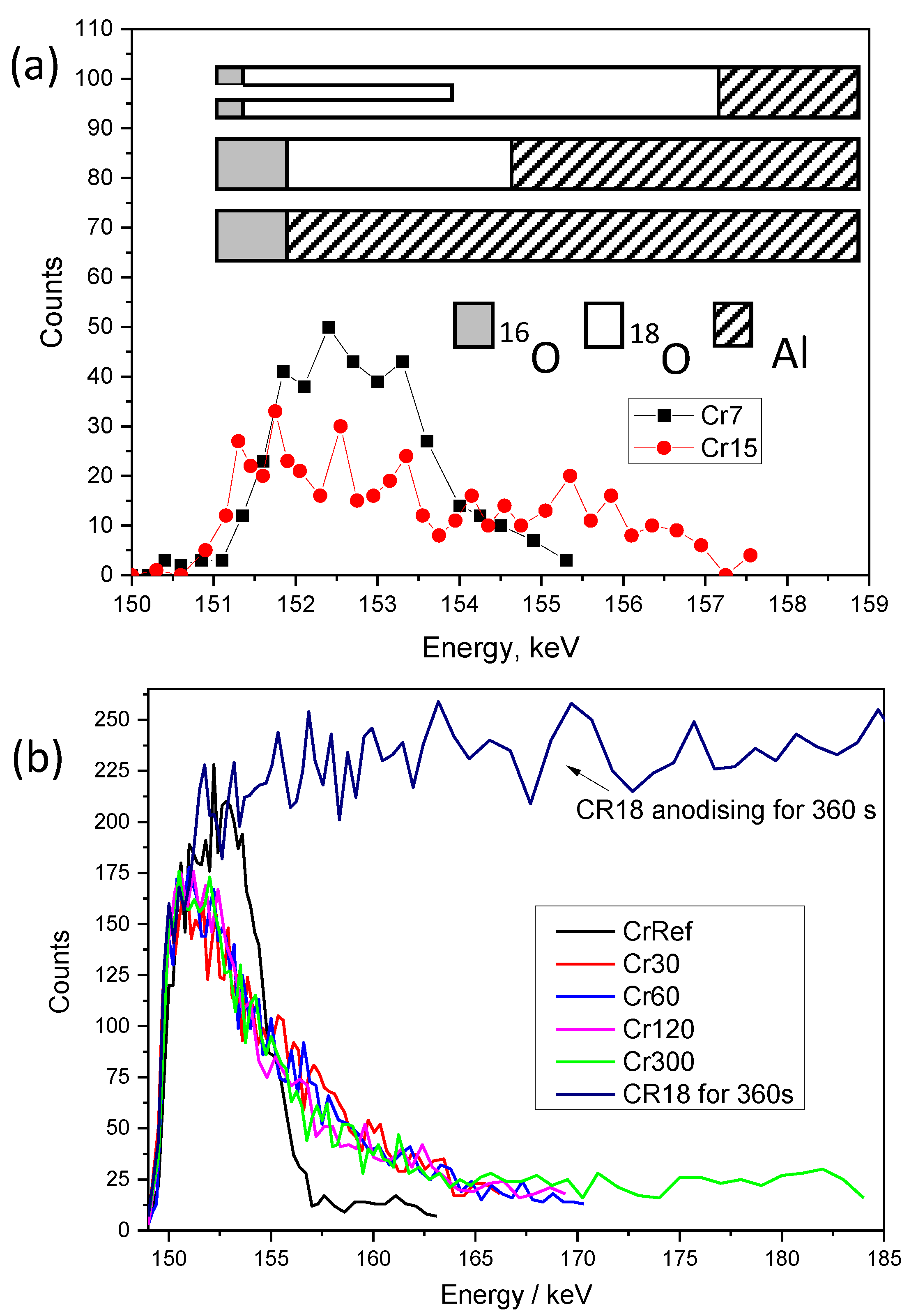
3.5. Re-Anodising in Chromic Acid—Chemical Composition of Film from NRA and RBS
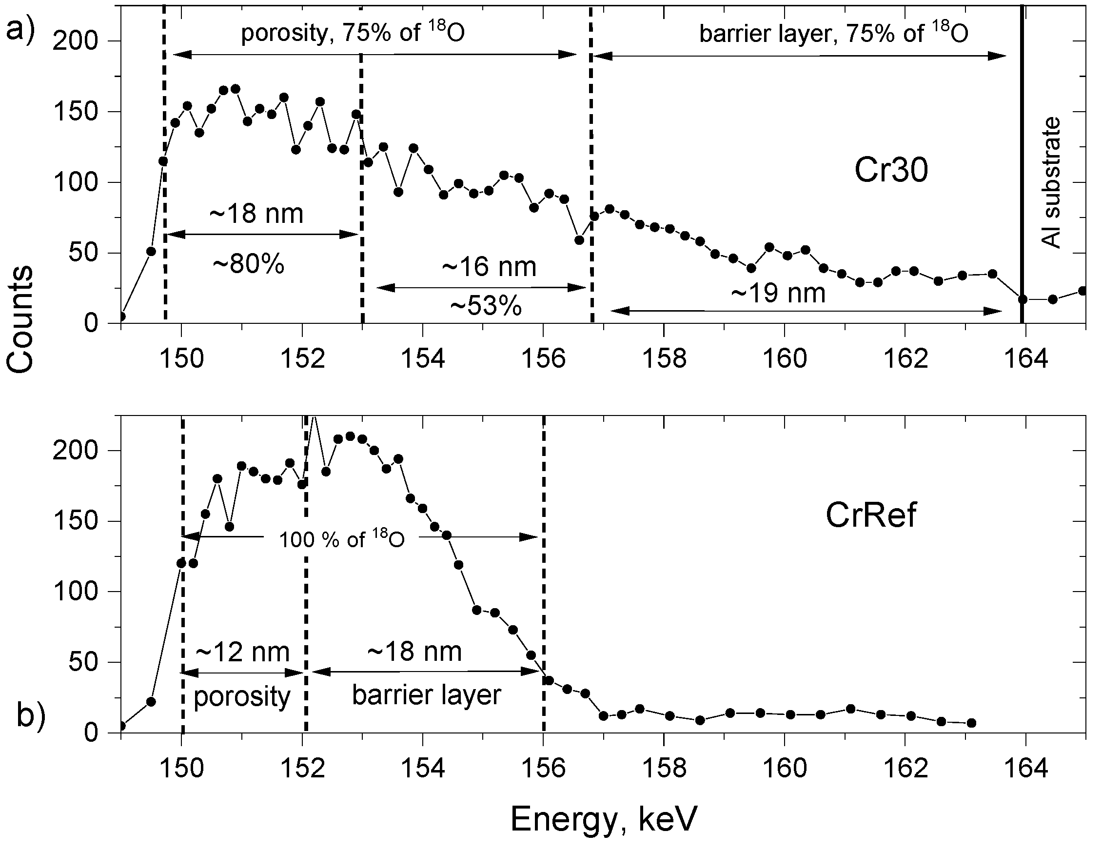
3.6. 18O Species Distribution Profile in Films
4. Conclusions
Author Contributions
Funding
Data Availability Statement
Acknowledgments
Conflicts of Interest
References
- Keller, F.; Hunter, M.; Robinson, D. Structural features of oxide coatings on aluminum. J. Electrochem. Soc. 1953, 100, 411. [Google Scholar] [CrossRef]
- Hoar, T.; Mott, N. A mechanism for the formation of porous anodic oxide films on aluminium. J. Phys. Chem. Solids 1959, 9, 97–99. [Google Scholar] [CrossRef]
- Diggle, J.W.; Downie, T.; Goulding, C. Processes Involved in Reattainment of Steady-State Conditions for the Anodizing of Aluminum Following Formation Voltage Changes. J. Electrochem. Soc. 1969, 116, 737. [Google Scholar] [CrossRef]
- O’sullivan, J.; Wood, G. The morphology and mechanism of formation of porous anodic films on aluminium. Proc. R. Soc. London A. Math. Phys. Sci. 1970, 317, 511–543. [Google Scholar]
- Garcia-Vergara, S.; Skeldon, P.; Thompson, G.; Habazaki, H. A flow model of porous anodic film growth on aluminium. Electrochim. Acta 2006, 52, 681–687. [Google Scholar] [CrossRef]
- Skeldon, P.; Thompson, G.; Garcia-Vergara, S.; Iglesias-Rubianes, L.; Blanco-Pinzon, C. A tracer study of porous anodic alumina. Electrochem. Solid-State Lett. 2006, 9, B47. [Google Scholar] [CrossRef]
- Mercier, D.; Van Overmeere, Q.; Santoro, R.; Proost, J. In-situ optical emission spectrometry during galvanostatic aluminum anodising. Electrochim. Acta 2011, 56, 1329–1336. [Google Scholar] [CrossRef]
- Van Overmeere, Q.; Mercier, D.; Santoro, R.; Proost, J. In situ optical emission spectrometry during porous anodic alumina initiation and growth in phosphoric acid. Electrochem. Solid-State Lett. 2011, 15, C1. [Google Scholar] [CrossRef]
- Garcia-Vergara, S.; Le Clere, D.; Hashimoto, T.; Habazaki, H.; Skeldon, P.; Thompson, G. Optimized observation of tungsten tracers for investigation of formation of porous anodic alumina. Electrochim. Acta 2009, 54, 6403–6411. [Google Scholar] [CrossRef]
- Shimizu, K.; Brown, G.M.; Habazaki, H.; Kobayashi, K.; Skeldon, P.; Thompson, G.E.; Wood, G.C. Glow discharge optical emission spectrometry (GDOES) depth profiling analysis of anodic alumina films—A depth resolution study. Surf. Interface Anal. 1999, 27, 24–28. [Google Scholar] [CrossRef]
- Baron Wiecheć, A.; Tempez, A.; Skeldon, P.; Chapon, P.; Thompson, G. 18O distributions in porous anodic alumina by plasma profiling time-of-flight mass spectrometry and nuclear reaction analysis. Surf. Interface Anal. 2012, 44, 1346–1352. [Google Scholar] [CrossRef]
- Bustelo, M.; Fernandez, B.; Pisonero, J.; Pereiro, R.; Bordel, N.; Vega, V.; Prida, V.M.; Sanz-Medel, A. Pulsed radiofrequency glow discharge time-of-flight mass spectrometry for nanostructured materials characterization. Anal. Chem. 2011, 83, 329–337. [Google Scholar] [CrossRef] [PubMed]
- Curioni, M.; Koroleva, E.; Skeldon, P.; Thompson, G. Flow modulated ionic migration during porous oxide growth on aluminium. Electrochim. Acta 2010, 55, 7044–7049. [Google Scholar] [CrossRef]
- Garcia-Vergara, S.; Skeldon, P.; Thompson, G.; Habakaki, H. Tracer studies of anodic films formed on aluminium in malonic and oxalic acids. Appl. Surf. Sci. 2007, 254, 1534–1542. [Google Scholar] [CrossRef]
- Garcia-Vergara, S.; Habazaki, H.; Skeldon, P.; Thompson, G. Formation of porous anodic alumina at high current efficiency. Nanotechnology 2007, 18, 415605. [Google Scholar] [CrossRef]
- Zhou, F.-y.; Al-Zenati, A.M.; Baron-Wiecheć, A.; Curioni, M.; Garcia-Vergara, S.; Habazaki, H.; Skeldon, P.; Thompson, G. Volume expansion factor and growth efficiency of anodic alumina formed in sulphuric acid. J. Electrochem. Soc. 2011, 158, C202. [Google Scholar] [CrossRef]
- Baron-Wiecheć, A.; Ganem, J.; Garcia-Vergara, S.; Skeldon, P.; Thompson, G.; Vickridge, I. # 2# 1 Tracer Study of Porous Film Growth on Aluminum in Phosphoric Acid. J. Electrochem. Soc. 2010, 157, C399. [Google Scholar]
- Baron-Wiecheć, A.; Ekundayo, O.; Garcia-Vergara, S.; Habazaki, H.; Liu, H.; Skeldon, P.; Thompson, G. Ion Migration and Film Morphologies in Anodic Alumina Films Formed in Selenate Electrolyte. J. Electrochem. Soc. 2012, 159, C312. [Google Scholar] [CrossRef]
- Baron-Wiecheć, A.; Skeldon, P.; Ganem, J.-J.; Vickridge, I.; Thompson, G. Porous anodic alumina growth in borax electrolyte. J. Electrochem. Soc. 2012, 159, C583. [Google Scholar] [CrossRef]
- Baron-Wiecheć, A.; Burke, M.; Hashimoto, T.; Liu, H.; Skeldon, P.; Thompson, G.; Habazaki, H.; Ganem, J.-J.; Vickridge, I. Tracer study of pore initiation in anodic alumina formed in phosphoric acid. Electrochim. Acta 2013, 113, 302–312. [Google Scholar] [CrossRef]
- Muratore, F.; Baron-Wiecheć, A.; Hashimoto, T.; Skeldon, P.; Thompson, G. Anodic zirconia nanotubes: Composition and growth mechanism. Electrochem. Commun. 2010, 12, 1727–1730. [Google Scholar] [CrossRef]
- Matykina, E.; Arrabal, R.; Scurr, D.; Baron, A.; Skeldon, P.; Thompson, G. Investigation of the mechanism of plasma electrolytic oxidation of aluminium using 18O tracer. Corros. Sci. 2010, 52, 1070–1076. [Google Scholar] [CrossRef]
- Houser, J.E.; Hebert, K.R. The role of viscous flow of oxide in the growth of self-ordered porous anodic alumina films. Nat. Mater. 2009, 8, 415–420. [Google Scholar] [CrossRef] [PubMed]
- Hebert, K.R.; Albu, S.P.; Paramasivam, I.; Schmuki, P. Morphological instability leading to formation of porous anodic oxide films. Nat. Mater. 2012, 11, 162–166. [Google Scholar] [CrossRef] [PubMed]
- Elabar, D.; Němcová, A.; Hashimoto, T.; Skeldon, P.; Thompson, G. Effect of sulphate impurity in chromic acid anodizing of aluminium. Corros. Sci. 2015, 100, 377–385. [Google Scholar] [CrossRef]
- Elabar, D.; Hashimoto, T.; Qi, J.; Skeldon, P.; Thompson, G. Effect of low levels of sulphate on the current density and film morphology during anodizing of aluminium in chromic acid. Electrochim. Acta 2016, 196, 206–222. [Google Scholar] [CrossRef]
- Volnianska, O.; Boguslawski, P. Magnetism of solids resulting from spin polarization of p orbitals. J. Phys. Condens. Matter 2010, 22, 073202. [Google Scholar] [CrossRef] [PubMed]
- Ogale, S.B. Dilute doping, defects, and ferromagnetism in metal oxide systems. Adv. Mater. 2010, 22, 3125–3155. [Google Scholar] [CrossRef]
- Stoneham, M. The strange magnetism of oxides and carbons. J. Phys. Condens. Matter 2010, 22, 074211. [Google Scholar] [CrossRef]
- Schirmer, O.F. O− bound small polarons in oxide materials. J. Phys. Condens. Matter 2006, 18, R667. [Google Scholar] [CrossRef]
- Takahashi, H.; Nagayama, M. The determination of the porosity of anodic oxide films on aluminium by the pore-filling method. Corros. Sci. 1978, 18, 911–925. [Google Scholar] [CrossRef]
- Mayer, M.; Eckstein, W.; Langhuth, H.; Schiettekatte, F.; Von Toussaint, U. Computer simulation of ion beam analysis: Possibilities and limitations. Nucl. Instrum. Methods Phys. Res. Sect. B Beam Interact. Mater. At. 2011, 269, 3006–3013. [Google Scholar] [CrossRef][Green Version]
- Amsel, G.; Samuel, D. Microanalysis of the stable isotopes of oxygen by means of nuclear reactions. Anal. Chem. 1967, 39, 1689–1698. [Google Scholar] [CrossRef]
- Battistig, G.; Amsel, G.; d’Artemare, E.; Vickridge, I. A very narrow resonance in 18O (p, α) 15 N near 150 keV: Application to isotopic tracing: I. Resonance width measurement. Nucl. Instrum. Methods Phys. Res. Sect. B Beam Interact. Mater. At. 1991, 61, 369–376. [Google Scholar] [CrossRef]
- Battistig, G.; Amsel, G.; d’Artemare, E.; Vickridge, I. A very narrow resonance in 18O (p, α) 15 N near 150 keV: Application to isotopic tracing. II. High resolution depth profiling of 18O. Nucl. Instrum. Methods Phys. Res. Sect. B Beam Interact. Mater. At. 1992, 66, 1–10. [Google Scholar] [CrossRef]
- Shimizu, K.; Thompson, G.; Wood, G. The duplex nature of anodic barrier films formed on aluminium in aqueous borate and borate-glycol solutions. Thin Solid Film. 1981, 85, 53–59. [Google Scholar] [CrossRef]
- Thompson, G.; Furneaux, R.; Wood, G. Electron microscopy of ion beam thinned porous anodic films formed on aluminium. Corros. Sci. 1978, 18, 481–498. [Google Scholar] [CrossRef]
- Ono, S.; Ichinose, H.; Kawaguchi, T.; Masuko, N. The observation of anodic oxide films on aluminum by high resolution electron microscopy. Corros. Sci. 1990, 31, 249–254. [Google Scholar] [CrossRef]
- Vrublevsky, I.; Jagminas, A.; Schreckenbach, J.; Goedel, W. Embedded space charge in porous alumina films formed in phosphoric acid. Electrochim. Acta 2007, 53, 300–304. [Google Scholar] [CrossRef]
- Vickridge, I.; Amsel, G. SPACES: A PC implementation of the stochastic theory of energy loss for narrow-resonance depth profiling. Nucl. Instrum. Methods Phys. Res. Sect. B Beam Interact. Mater. At. 1990, 45, 6–11. [Google Scholar] [CrossRef]
- Ziegler, J.F.; Ziegler, M.D.; Biersack, J.P. SRIM–The stopping and range of ions in matter (2010). Nucl. Instrum. Methods Phys. Res. Sect. B Beam Interact. Mater. At. 2010, 268, 1818–1823. [Google Scholar] [CrossRef]
- Morlidge, J.; Skeldon, P.; Thompson, G.; Habazaki, H.; Shimizu, K.; Wood, G. Gel formation and the efficiency of anodic film growth on aluminium. Electrochim. Acta 1999, 44, 2423–2435. [Google Scholar] [CrossRef]
- Oh, J.; Thompson, C.V. Abnormal anodic aluminum oxide formation in confined structures for lateral pore arrays. J. Electrochem. Soc. 2011, 158, C71. [Google Scholar] [CrossRef]
- Lambert, J.; Guthmann, C.; Ortega, C.; Saint-Jean, M. Permanent polarization and charge injection in thin anodic alumina layers studied by electrostatic force microscopy. J. Appl. Phys. 2002, 91, 9161–9169. [Google Scholar] [CrossRef]
- Proost, J. Mechanical and Electrostrictive Effects in Anodic Films. In Encyclopedia of Interfacial Chemistry: Surface Science and Electrochemistry; Elsevier: Amsterdam, The Netherlands, 2017. [Google Scholar]
- Curioni, M.; Scenini, F. The mechanism of hydrogen evolution during anodic polarization of aluminium. Electrochim. Acta 2015, 180, 712–721. [Google Scholar] [CrossRef]
- DeWitt, S.; Thornton, K. Simulations of Anodic Nanopore Growth Using the Smoothed Boundary and Level Set Methods. J. Phys. Chem. C 2016, 120, 2419–2431. [Google Scholar] [CrossRef]
- Iglesias-Rubianes, L.; Skeldon, P.; Thompson, G.; Kreissig, U.; Grambole, D.; Habazaki, H.; Shimizu, K. Behaviour of hydrogen impurity in aluminium alloys during anodizing. Thin Solid Film. 2003, 424, 201–207. [Google Scholar] [CrossRef]
- Ono, S.; Asoh, H. A new perspective on pore growth in anodic alumina films. Electrochem. Commun. 2021, 124, 106972. [Google Scholar] [CrossRef]
- Pilling, N. The oxidation of metals at high temperature. J. Inst. Met. 1923, 29, 529–582. [Google Scholar]


| Experiment Ar18–Cr16 | Experiment Cr18–Cr16 | ||||||||
|---|---|---|---|---|---|---|---|---|---|
| Sample Name | Re-Anodizing Time, s/Voltage (V) | Film Thickness | Exp. Factor | Sample Name | Re-Anodizing Time, s/Voltage (V) | Film Thickness | Exp. Factor | ||
| Barrier | Total | Barrier | Total | ||||||
| ArRef | 8/20 * | 25 | 1.80 | CrRef * | 28/15 | 19 | 31 | 1.08 | |
| Ar23 | 23/30 | 35 | 50 | 1.07 | Cr30 | 30/19 | 23 | 62 | 1.06 |
| Ar120 | 120/60 | 65 | 142 | 0.96 | Cr60 | 60/16.6 | 21 | 91 | 1.00 |
| Ar300 | 300/40 | 43 | 315 | 0.97 | Cr120 | 120/19 | 23 | 159 | 1.01 |
| Arim | 300/--- | Cr300 | 300/14.7 | 25 | 285 | 1.02 | |||
| Cr300im * | 300/--- | ||||||||
| Cr7ref * | 5/7 | 12.5 | --- | ||||||
| Cr15 | 7/15 | 13.5 | 31 | ||||||
| 16O * | 18O ** | 16O + 18O | Oxygen Increment | 18O Enrichment in the Ref | 18O Lost | Charge Passed, Q | Al Oxidised | ||
|---|---|---|---|---|---|---|---|---|---|
| Sample | 1015 Atoms/cm2 | % | mC/cm2 | nm | % | ||||
| CrRef | 130.9 | 11.4 | 142.29 | 142.29 | 8.01 | 81.57 | 27.73 | 55 | |
| Cr30 | 271.8 | 11.7 | 283.48 | 141.19 | 0 | 85.00 | 28.9 | 54 | |
| Cr60 | 365.9 | 12 | 377.86 | 233.35 | 8.68 | 4.5 | 167.00 | 56.78 | 45 |
| Cr120 | 652.8 | 11.7 | 664.5 | 508.08 | 7.85 | 4.4 | 354.00 | 120 | 42 |
| Cr300 | 1086.3 | 10.4 | 1096.75 | 964.79 | 8.09 | 2.5 | 810.00 | 275 | 31 |
| CrRef | 137.9 | 12.5 | 150.42 | 150.42 | 8.3 | 94.56 | 32 | ||
| Crim | 128.7 | 11.1 | 139.25 | 7.22 | |||||
| CR18_360 | 1430 | 120 | 1742.15 | 1742.15 | 8.4 | 1081.00 | |||
| 16O * | 18O ** | 16O + 18O | 18O Enrichment | Oxygen Increment | 18O Lost | As | As Lost | Charge Passed, Q | Al Oxidised | ||
|---|---|---|---|---|---|---|---|---|---|---|---|
| Sample | 1015 Atoms/cm2% | 1015 Atoms/cm2 | 1015 Atoms/cm2 | % | mC/cm2 | nm | % | ||||
| ArRef | 102.6 | 10.6 (10.61–11.36) | 123.155 | 9.23 | 123.155 | 0.47 | 1.52 | 37 | 24 | 13 | 95 |
| Ar30 | 202.3 | 10.1 | 212.45 | 8.34 | 96.2 | 4.83 | 0.49 | 67 | 71.6 | 24 | 43 |
| Ar60 | 647.0 | 10.1 | 657.13 | 8.3 | 529.81 | 7.49 | 0.46 | 68 | 357.0 | 121 | 47 |
| Ar120 | 1440 | 9.9 | 1450.81 | 9.23 | 1322.6 | 6.12 | 0.4 | 71 | 888.0 | 301 | 48 |
| Arim | 108.8 | 11.3 | 120.071 | 9.42 | 3.47 | 1.16 | 37 | ||||
Disclaimer/Publisher’s Note: The statements, opinions and data contained in all publications are solely those of the individual author(s) and contributor(s) and not of MDPI and/or the editor(s). MDPI and/or the editor(s) disclaim responsibility for any injury to people or property resulting from any ideas, methods, instructions or products referred to in the content. |
© 2023 by the authors. Licensee MDPI, Basel, Switzerland. This article is an open access article distributed under the terms and conditions of the Creative Commons Attribution (CC BY) license (https://creativecommons.org/licenses/by/4.0/).
Share and Cite
Baron-Wiechec, A.; Lin, G. Isotopic Tracer Study of Initiation of Porosity in Anodic Alumina Formed in Chromic Acid. Nanomaterials 2024, 14, 42. https://doi.org/10.3390/nano14010042
Baron-Wiechec A, Lin G. Isotopic Tracer Study of Initiation of Porosity in Anodic Alumina Formed in Chromic Acid. Nanomaterials. 2024; 14(1):42. https://doi.org/10.3390/nano14010042
Chicago/Turabian StyleBaron-Wiechec, Aleksandra, and Guocong Lin. 2024. "Isotopic Tracer Study of Initiation of Porosity in Anodic Alumina Formed in Chromic Acid" Nanomaterials 14, no. 1: 42. https://doi.org/10.3390/nano14010042
APA StyleBaron-Wiechec, A., & Lin, G. (2024). Isotopic Tracer Study of Initiation of Porosity in Anodic Alumina Formed in Chromic Acid. Nanomaterials, 14(1), 42. https://doi.org/10.3390/nano14010042