
Structural, Electrical, and Optical Properties of Single-Walled Carbon Nanotubes Synthesized through Floating Catalyst Chemical Vapor Deposition

 , , , ,
Abstract
:1. Introduction
2. Experimental
2.1. Materials
2.2. SWCNTs Synthesis
2.3. SWCNT Characterization
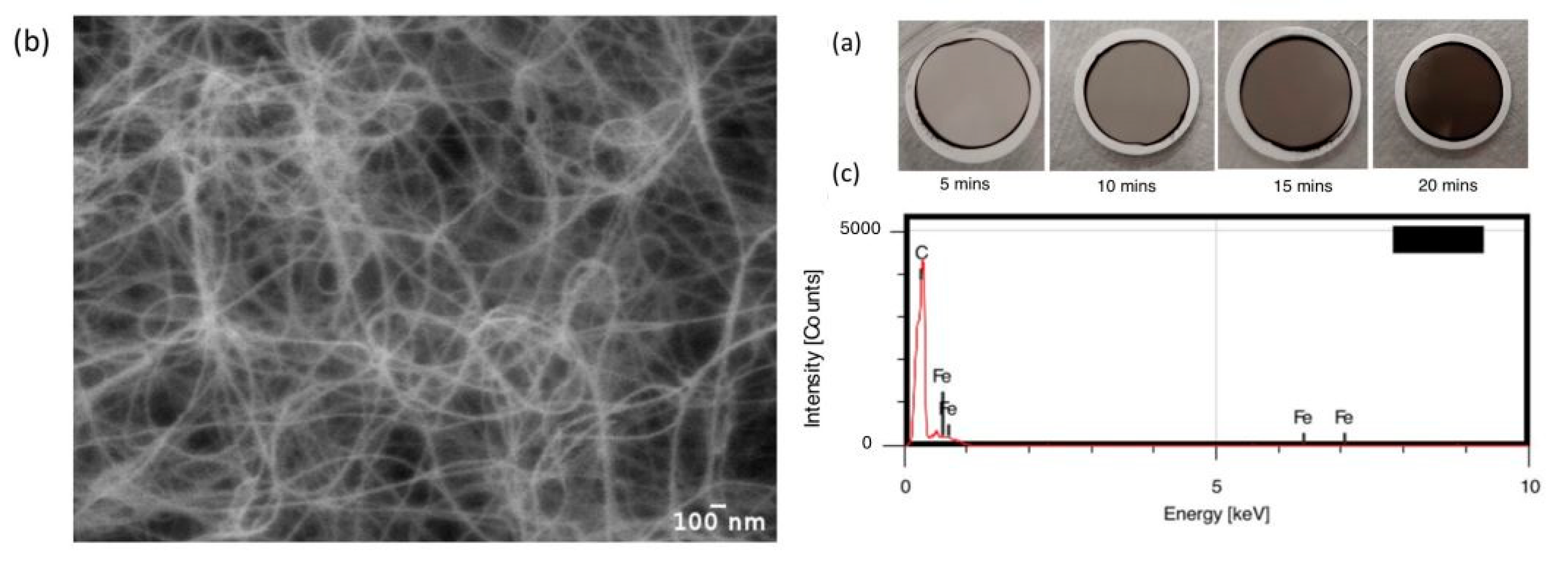
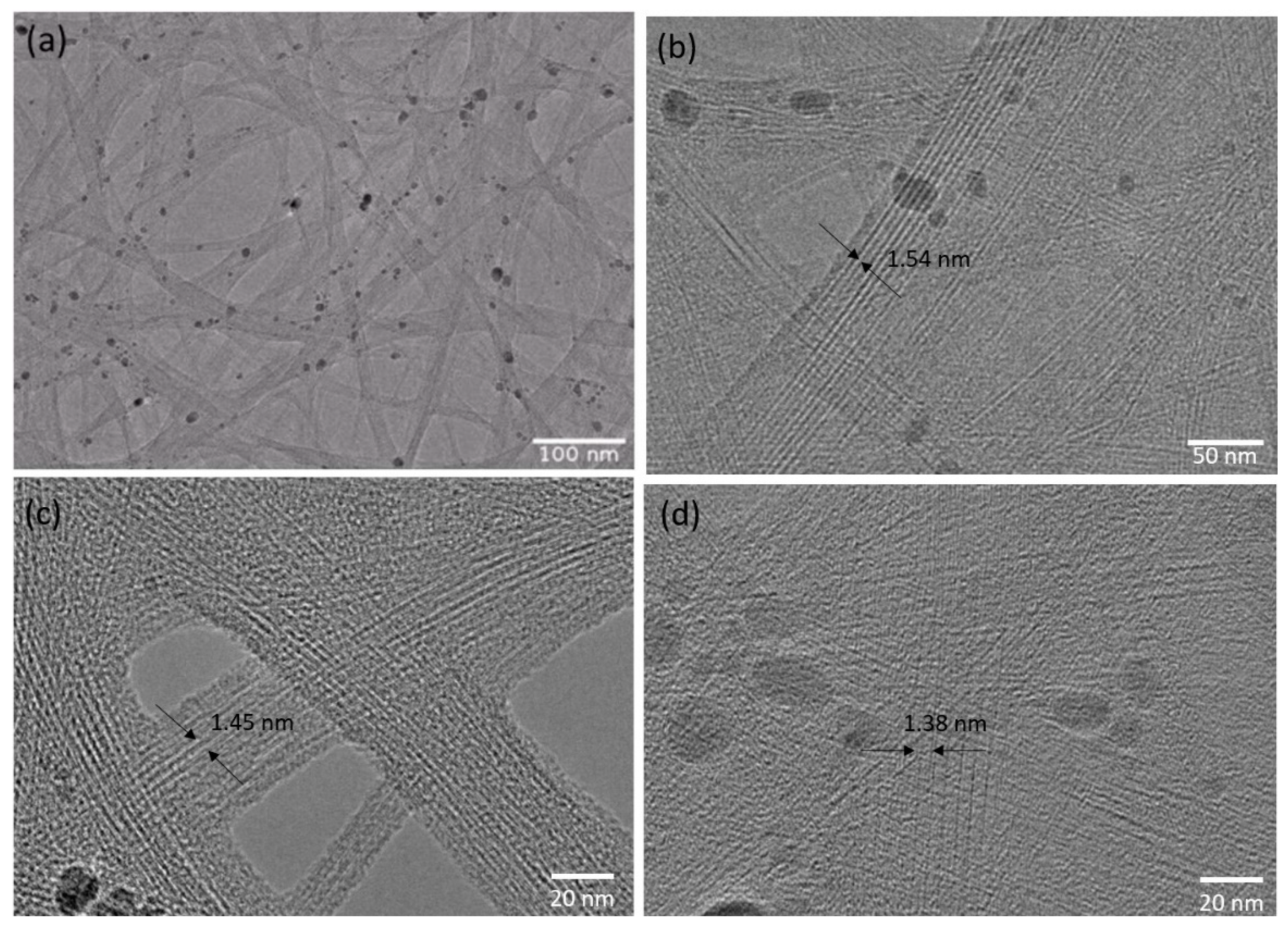
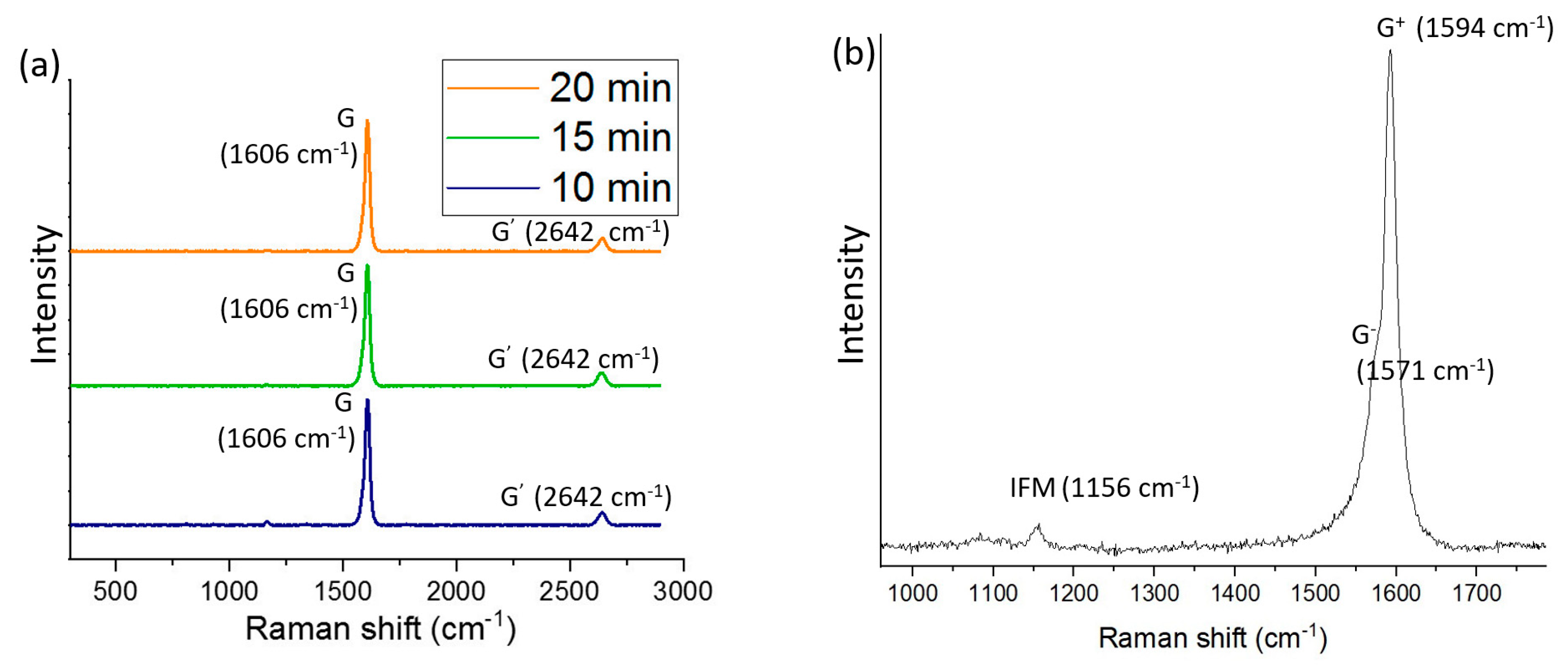
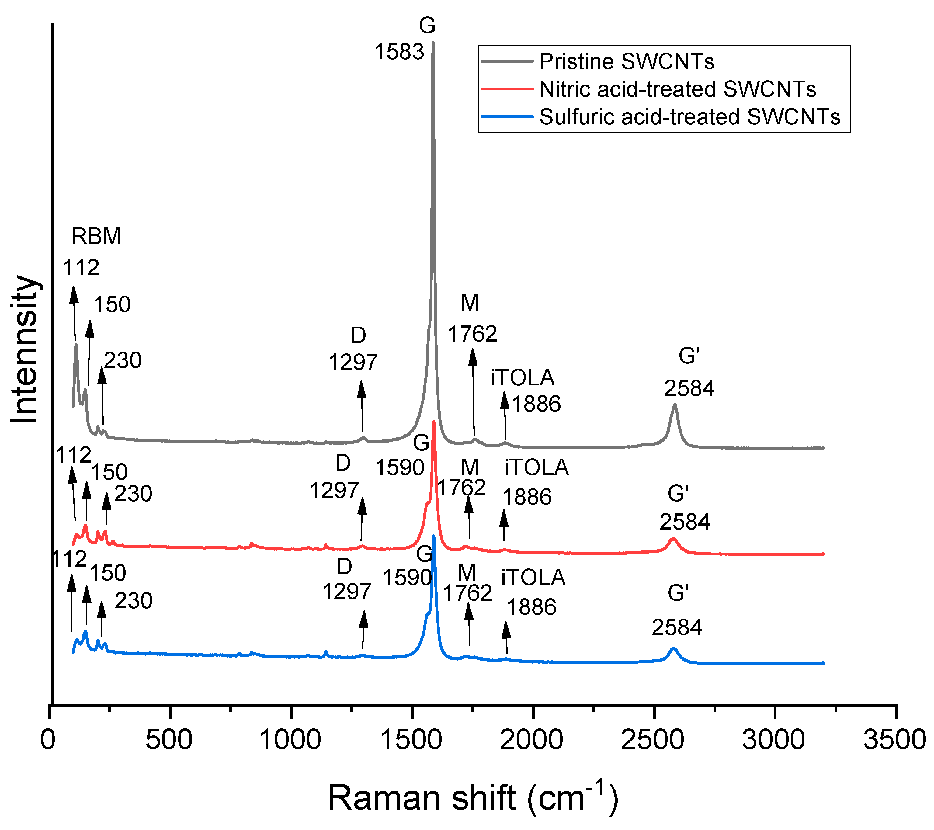
3. Results and Discussions
4. Conclusions
Author Contributions
Funding
Data Availability Statement
Acknowledgments
Conflicts of Interest
References
- Maruyama, T. Carbon nanotubes. In Handbook of Carbon-Based Nanomaterials; Elsevier: Amsterdam, The Netherlands, 2021; pp. 299–319. [Google Scholar]
- Dresselhaus, M.S.; Avouris, P. Introduction to carbon materials research. In Carbon Nanotubes: Synthesis, Structure, Properties, and Applications; Springer: Berlin/Heidelberg, Germany, 2001; pp. 1–9. [Google Scholar]
- Iijima, S. Helical microtubules of graphitic carbon. Nature 1991, 354, 56–58. [Google Scholar] [CrossRef]
- Iijima, S.; Ichihashi, T. Single-shell carbon nanotubes of 1-nm diameter. Nature 1993, 363, 603–605. [Google Scholar] [CrossRef]
- Rezaee, M.D.; Dahal, B.; Li, W. Single-Walled Carbon Nanotubes; American Chemical Society: Washington, DC, USA, 2023. [Google Scholar]
- Wu, K.; Niu, Y.; Zhang, Y.; Yong, Z.; Li, Q. Continuous growth of carbon nanotube films: From controllable synthesis to real applications. Compos. Part A Appl. Sci. Manuf. 2021, 144, 106359. [Google Scholar] [CrossRef]
- Di, J.; Wang, X.; Xing, Y.; Zhang, Y.; Zhang, X.; Lu, W.; Zhu, Y.T. Dry-Processable Carbon Nanotubes for Functional Devices and Composites. Small 2014, 10, 4606–4625. [Google Scholar] [CrossRef] [PubMed]
- Liu, L.; Ma, W.; Zhang, Z. Macroscopic carbon nanotube assemblies: Preparation, properties, and potential applications. Small 2011, 7, 1504–1520. [Google Scholar] [CrossRef] [PubMed]
- Peng, B.; Locascio, M.; Zapol, P.; Li, S.; Mielke, S.L.; Schatz, G.C.; Espinosa, H.D. Measurements of near-ultimate strength for multiwalled carbon nanotubes and irradiation-induced crosslinking improvements. Nat. Nanotechnol. 2008, 3, 626–631. [Google Scholar] [CrossRef] [PubMed]
- Bai, Y.; Zhang, R.; Ye, X.; Zhu, Z.; Xie, H.; Shen, B.; Wei, F. Carbon nanotube bundles with tensile strength over 80 GPa. Nat. Nanotechnol. 2018, 13, 589–595. [Google Scholar] [CrossRef] [PubMed]
- Chen, H.; Zeng, S.; Chen, M.; Zhang, Y.; Li, Q. Fabrication and functionalization of carbon nanotube films for high-performance flexible supercapacitors. Carbon 2015, 92, 271–296. [Google Scholar] [CrossRef]
- Zhou, Y.; Azumi, R. Carbon nanotube based transparent conductive films: Progress, challenges, and perspectives. Sci. Technol. Adv. Mater. 2016, 17, 493–516. [Google Scholar] [CrossRef]
- Liao, Y.; Hussain, A.; Laiho, P.; Zhang, Q.; Tian, Y.; Wei, N.; Kauppinen, E.I. Tuning Geometry of SWCNTs by CO2 in Floating Catalyst CVD for High-Performance Transparent Conductive Films. Adv. Mater. Interfaces 2018, 5, 1801209. [Google Scholar] [CrossRef]
- Meysami, S.S.; Koos, A.A.; Dillon, F.; Grobert, N. Aerosol-assisted chemical vapour deposition synthesis of multi-wall carbon nanotubes: II. Anal. Study Carbon 2013, 58, 159–169. [Google Scholar] [CrossRef]
- Choi, Y.C.; Bae, D.J.; Lee, Y.H.; Lee, B.S.; Park, G.S.; Choi, W.B.; Kim, J.M. Growth of carbon nanotubes by microwave plasma-enhanced chemical vapor deposition at low temperature. J. Vac. Sci. Technol. A Vac. Surf. Film. 2000, 18, 1864–1868. [Google Scholar] [CrossRef]
- Makris, T.D.; Giorgi, R.; Lisi, N.; Pilloni, L.; Salernitano, E.; Sarto, F.; Alvisi, M. Carbon nanotubes growth by HFCVD: Effect of the process parameters and catalyst preparation. Diam. Relat. Mater. 2004, 13, 305–310. [Google Scholar] [CrossRef]
- Byon, H.R.; Lim, H.S.; Song, H.J.; Choi, H.C. A synthesis of high purity single-walled carbon nanotubes from small diameters of cobalt nanoparticles by using oxygen-assisted chemical vapor deposition process. Bull. Korean Chem. Soc. 2007, 28, 2056–2060. [Google Scholar]
- Feng, C.; Liu, K.; Wu, J.S.; Liu, L.; Cheng, J.S.; Zhang, Y.; Jiang, K. Flexible, stretchable, transparent conducting films made from superaligned carbon nanotubes. Adv. Funct. Mater. 2010, 20, 885–891. [Google Scholar] [CrossRef]
- Bronikowski, M.J.; Willis, P.A.; Colbert, D.T.; Smith, K.A.; Smalley, R.E. Gas-phase production of carbon single-walled nanotubes from carbon monoxide via the HiPco process: A parametric study. J. Vac. Sci. Technol. A Vac. Surf. Film. 2001, 19, 1800–1805. [Google Scholar] [CrossRef]
- Zhang, Q.; Wei, N.; Laiho, P.; Kauppinen, E.I. Recent developments in single-walled carbon nanotube thin films fabricated by dry floating catalyst chemical vapor deposition. In Single-Walled Carbon Nanotubes: Preparation, Properties and Applications; Springer: Berlin/Heidelberg, Germany, 2019; pp. 99–128. [Google Scholar]
- Bogdanova, A.R.; Krasnikov, D.V.; Nasibulin, A.G. The role of sulfur in the CVD carbon nanotube synthesis. Carbon 2023, 210, 118051. [Google Scholar] [CrossRef]
- Chen, D.R.; Chitranshi, M.; Schulz, M.; Shanov, V. A review of three major factors controlling carbon nanotubes synthesis from the floating catalyst chemical vapor deposition. Nano Life 2019, 9, 1930002. [Google Scholar] [CrossRef]
- Yu, F.; Yang, M.; Li, F.; Su, C.; Ma, B.; Yuan, Z.; Ma, J. The growth mechanism of single-walled carbon nanotubes with a controlled diameter. Phys. E Low-Dimens. Syst. Nanostruct. 2012, 44, 2032–2040. [Google Scholar] [CrossRef]
- Plata, D.L.; Meshot, E.R.; Reddy, C.M.; Hart, A.J.; Gschwend, P.M. Multiple alkynes react with ethylene to enhance carbon nanotube synthesis, suggesting a polymerization-like formation mechanism. ACS Nano 2010, 4, 7185–7192. [Google Scholar] [CrossRef]
- Huang, S.; Cai, Q.; Chen, J.; Qian, Y.; Zhang, L. Metal-catalyst-free growth of single-walled carbon nanotubes on substrates. J. Am. Chem. Soc. 2009, 131, 2094–2095. [Google Scholar] [CrossRef] [PubMed]
- Li, Y.; Ji, K.; Duan, Y.; Meng, G.; Dai, Z. Effect of hydrogen concentration on the growth of carbon nanotube arrays for gecko-inspired adhesive applications. Coatings 2017, 7, 221. [Google Scholar] [CrossRef]
- Ma, Y.; Dichiara, A.B.; He, D.; Zimmer, L.; Bai, J. Control of product nature and morphology by adjusting the hydrogen content in a continuous chemical vapor deposition process for carbon nanotube synthesis. Carbon 2016, 107, 171–179. [Google Scholar] [CrossRef]
- Kumar, A.; Kostikov, Y.; Zanatta, M.; Sorarù, G.D.; Orberger, B.; Nessim, G.D.; Mariotto, G. Carbon nanotubes synthesis using siliceous breccia as a catalyst source. Diam. Relat. Mater. 2019, 97, 107433. [Google Scholar] [CrossRef]
- Graupner, R.; Abraham, J.; Vencelová, A.; Seyller, T.; Hennrich, F.; Kappes, M.M.; Ley, L. Doping of single-walled carbon nanotube bundles by Brønsted acids. Phys. Chem. Chem. Phys. 2003, 5, 5472–5476. [Google Scholar] [CrossRef]
- Dresselhaus, M.S.; Dresselhaus, G. Intercalation compounds of graphite. Adv. Phys. 1981, 30, 139–326. [Google Scholar] [CrossRef]
- Zhou, Y.; Shimada, S.; Saito, T.; Azumi, R. Understanding the doping effects on the structural and electrical properties of ultrathin carbon nanotube networks. J. Appl. Phys. 2015, 118, 215305. [Google Scholar] [CrossRef]
- Barros, E.B.; Son, H.; Samsonidze, G.G.; Souza Filho, A.G.; Saito, R.; Kim, Y.A.; Dresselhaus, M.S. Raman spectroscopy of double-walled carbon nanotubes treated with H2SO4. Phys. Rev. B 2007, 76, 045425. [Google Scholar] [CrossRef]
- Rao, A.M.; Eklund, P.C.; Bandow, S.; Thess, A.; Smalley, R.E. Evidence for charge transfer in doped carbon nanotube bundles from Raman scattering. Nature 1997, 388, 257–259. [Google Scholar] [CrossRef]
- Fagan, S.B.; Souza Filho, A.G.D.; Mendes Filho, J.; Corio, P.; Dresselhaus, M.S. Electronic properties of Ag-and CrO3-filled single-wall carbon nanotubes. Chem. Phys. Lett. 2005, 406, 54–59. [Google Scholar] [CrossRef]
- Ding, E.X.; Jiang, H.; Zhang, Q.; Tian, Y.; Laiho, P.; Hussain, A.; Kauppinen, E.I. Highly conductive and transparent single-walled carbon nanotube thin films from ethanol by floating catalyst chemical vapor deposition. Nanoscale 2017, 9, 17601–17609. [Google Scholar] [CrossRef]
- Lee, S.H.; Uhm, T.W.; You, Y.G.; Kim, S.W.; Jhang, S.H.; Dettlaff-Weglikowska, U.; Park, Y.W. Hall effect in carbon nanotube thin films. Synth. Met. 2014, 198, 84–87. [Google Scholar] [CrossRef]
- Mintmire, J.W.; Dunlap, B.I.; White, C.T. Are fullerene tubules metallic? Phys. Rev. Lett. 1992, 68, 631. [Google Scholar] [CrossRef] [PubMed]
- Nakka, L.; Cheng, Y.; Aberle, A.G.; Lin, F. Analytical review of spiro-OMeTAD hole transport materials: Paths toward stable and efficient perovskite solar cells. Adv. Energy Sustain. Res. 2022, 3, 2200045. [Google Scholar] [CrossRef]
- Kaskela, A.; Laiho, P.; Fukaya, N.; Mustonen, K.; Susi, T.; Jiang, H.; Kauppinen, E.I. Highly individual SWCNTs for high performance thin film electronics. Carbon 2016, 103, 228–234. [Google Scholar] [CrossRef]
- Niu, Z.; Zhou, W.; Chen, J.; Feng, G.; Li, H.; Ma, W.; Xie, S. Compact-designed supercapacitors using free-standing single-walled carbon nanotube films. Energy Environ. Sci. 2011, 4, 1440–1446. [Google Scholar] [CrossRef]
- Ma, W.; Song, L.; Yang, R.; Zhang, T.; Zhao, Y.; Sun, L.; Xie, S. Directly synthesized strong, highly conducting, transparent single-walled carbon nanotube films. Nano Lett. 2007, 7, 2307–2311. [Google Scholar] [CrossRef]
- Hussain, A.; Liao, Y.; Zhang, Q.; Ding, E.X.; Laiho, P.; Ahmad, S.; Kauppinen, E.I. Floating catalyst CVD synthesis of single walled carbon nanotubes from ethylene for high performance transparent electrodes. Nanoscale 2018, 10, 9752–9759. [Google Scholar] [CrossRef]
- A Shi, Z.; Lian, Y.; Liao, F.H.; Zhou, X.; Gu, Z.; Zhang, Y.; Zhang, S.L. Large scale synthesis of single-wall carbon nanotubes by arc-discharge method. J. Phys. Chem. Solids 2000, 61, 1031–1036. [Google Scholar] [CrossRef]
- Ajayan, P.M.; Ebbesen, T.W. Nanometre-size tubes of carbon. Rep. Prog. Phys. 1997, 60, 1025. [Google Scholar] [CrossRef]
- Ruoff, R.S.; Qian, D.; Liu, W.K. Mechanical properties of carbon nanotubes: Theoretical predictions and experimental measurements. Comptes Rendus Phys. 2003, 4, 993–1008. [Google Scholar] [CrossRef]
- Dresselhaus, M.S.; Dresselhaus, G.; Saito, R.; Jorio, A. Raman spectroscopy of carbon nanotubes. Phys. Rep. 2005, 409, 47–99. [Google Scholar] [CrossRef]
- Pimenta, M.A.; Dresselhaus, G.; Dresselhaus, M.S.; Cancado, L.G.; Jorio, A.; Saito, R. Studying disorder in graphite-based systems by Raman spectroscopy. Phys. Chem. Chem. Phys. 2007, 9, 1276–1290. [Google Scholar] [CrossRef] [PubMed]
- Ferrari, A.C.; Meyer, J.C.; Scardaci, V.; Casiraghi, C.; Lazzeri, M.; Mauri, F.; Geim, A.K. Raman spectrum of graphene and graphene layers. Phys. Rev. Lett. 2006, 97, 187401. [Google Scholar] [CrossRef] [PubMed]
- Park, Y.; Hembram, K.P.S.S.; Yoo, R.; Jang, B.; Lee, W.; Lee, S.G.; Lee, J.K. Reinterpretation of single-wall carbon nanotubes by Raman spectroscopy. J. Phys. Chem. C 2019, 123, 14003–14009. [Google Scholar] [CrossRef]
- Kim, K.K.; Park, J.S.; Kim, S.J.; Geng, H.Z.; An, K.H.; Yang, C.M.; Lee, Y.H. Dependence of Raman spectra G′ band intensity on metallicity of single-wall carbon nanotubes. Phys. Rev. B 2007, 76, 205426. [Google Scholar] [CrossRef]
- Lopez-Lorente, A.I.; Simonet, B.M.; Valcarcel, M. Qualitative detection and quantitative determination of single-walled carbon nanotubes in mixtures of carbon nanotubes with a portable Raman spectrometer. Analyst 2013, 138, 2378–2385. [Google Scholar] [CrossRef]
- Jorio, A.; Saito, R. Raman spectroscopy for carbon nanotube applications. J. Appl. Phys. 2021, 129, 021102. [Google Scholar] [CrossRef]
- Jorio, A.; Souza Filho, A.G.; Dresselhaus, G.; Dresselhaus, M.S.; Swan, A.K.; Ünlü, M.S.; Saito, R. G-band resonant Raman study of 62 isolated single-wall carbon nanotubes. Phys. Rev. B 2002, 65, 155412. [Google Scholar] [CrossRef]
- Kataura, H.; Kumazawa, Y.; Maniwa, Y.; Umezu, I.; Suzuki, S.; Ohtsuka, Y.; Achiba, Y. Optical properties of single-wall carbon nanotubes. Synth. Met. 1999, 103, 2555–2558. [Google Scholar] [CrossRef]
- Saito, R.; Jorio, A.; Souza Filho, A.G.; Dresselhaus, G.; Dresselhaus, M.S.; Pimenta, M.A. Probing phonon dispersion relations of graphite by double resonance Raman scattering. Phys. Rev. Lett. 2001, 88, 027401. [Google Scholar] [CrossRef] [PubMed]
- Saito, R.; Grüneis, A.; Samsonidze, G.G.; Brar, V.W.; Dresselhaus, G.; Dresselhaus, M.S.; Souza Filho, A.G. Double resonance Raman spectroscopy of single-wall carbon nanotubes. New J. Phys. 2003, 5, 157. [Google Scholar] [CrossRef]
- Wang, P.C.; Liao, Y.C.; Lai, Y.L.; Lin, Y.C.; Su, C.Y.; Tsai, C.H.; Hsu, Y.J. Conversion of pristine and p-doped sulfuric-acid-treated single-walled carbon nanotubes to n-type materials by a facile hydrazine vapor exposure process. Mater. Chem. Phys. 2012, 134, 325–332. [Google Scholar] [CrossRef]
- Tantang, H.; Ong, J.Y.; Loh, C.L.; Dong, X.; Chen, P.; Chen, Y.; Li, L.J. Using oxidation to increase the electrical conductivity of carbon nanotube electrodes. Carbon 2009, 47, 1867–1870. [Google Scholar] [CrossRef]
- Rao, R.; Reppert, J.; Podila, R.; Zhang, X.; Rao, A.M.; Talapatra, S.; Maruyama, B. Double resonance Raman study of disorder in CVD-grown single-walled carbon nanotubes. Carbon 2011, 49, 1318–1325. [Google Scholar] [CrossRef]
- Yomogida, Y.; Horiuchi, K.; Okada, R.; Kawai, H.; Ichinose, Y.; Nishidome, H.; Yanagi, K. Hall effect in gated single-wall carbon nanotube films. Sci. Rep. 2022, 12, 101. [Google Scholar] [CrossRef] [PubMed]
- Hall, E.H. On a new action of the magnet on electric currents. Am. J. Math. 1879, 2, 287–292. [Google Scholar] [CrossRef]
- Baumgartner, G.; Carrard, M.; Zuppiroli, L.; Bacsa, W.; de Heer, W.A.; Forró, L. Hall effect and magnetoresistance of carbon nanotube films. Phys. Rev. B 1997, 55, 6704. [Google Scholar] [CrossRef]
- Song, S.N.; Wang, X.K.; Chang, R.P.H.; Ketterson, J.B. Electronic properties of graphite nanotubules from galvanomagnetic effects. Phys. Rev. Lett. 1994, 72, 697. [Google Scholar] [CrossRef]
- Martel, R.; Schmidt, T.; Shea, H.R.; Hertel, T.; Avouris, P. Single-and multi-wall carbon nanotube field-effect transistors. Appl. Phys. Lett. 1998, 73, 2447–2449. [Google Scholar] [CrossRef]
- Dürkop, T.; Getty, S.A.; Cobas, E.; Fuhrer, M.S. Extraordinary mobility in semiconducting carbon nanotubes. Nano Lett. 2004, 4, 35–39. [Google Scholar] [CrossRef]
- Jiang, S.; Hou, P.X.; Liu, C.; Cheng, H.M. High-performance single-wall carbon nanotube transparent conductive films. J. Mater. Sci. Technol. 2019, 35, 2447–2462. [Google Scholar] [CrossRef]
- Hennrich, F.; Wellmann, R.; Malik, S.; Lebedkin, S.; Kappes, M.M. Reversible modification of the absorption properties of single-walled carbon nanotube thin films via nitric acid exposure. Phys. Chem. Chem. Phys. 2003, 5, 178–183. [Google Scholar] [CrossRef]
- Sumanasekera, G.U.; Allen, J.L.; Fang, S.L.; Loper, A.L.; Rao, A.M.; Eklund, P.C. Electrochemical oxidation of single wall carbon nanotube bundles in sulfuric acid. J. Phys. Chem. B 1999, 103, 4292–4297. [Google Scholar] [CrossRef]
- Paul, S.; Kang, Y.S.; Sun, Y.K.; Kim, D.W. Highly conductive and transparent thin films fabricated with predominantly semiconducting single-walled carbon nanotubes. Carbon 2010, 48, 2646–2649. [Google Scholar] [CrossRef]
- Earp, B.; Dunn, D.; Phillips, J.; Agrawal, R.; Ansell, T.; Aceves, P.; Luhrs, C. Enhancement of electrical conductivity of carbon nanotube sheets through copper addition using reduction expansion synthesis. Mater. Res. Bull. 2020, 131, 110969. [Google Scholar] [CrossRef]
- Kim, K.K.; Bae, J.J.; Park, H.K.; Kim, S.M.; Geng, H.Z.; Park, K.A.; Lee, Y.H. Fermi level engineering of single-walled carbon nanotubes by AuCl3 doping. J. Am. Chem. Soc. 2008, 130, 12757–12761. [Google Scholar] [CrossRef] [PubMed]
- Coates, J. Interpretation of infrared spectra, a practical approach. Encycl. Anal. Chem. 2000, 12, 10815–10837. [Google Scholar]
- Kamble, R.V.; Bhinge, S.D.; Mohite, S.K.; Randive, D.S.; Bhutkar, M.A. In vitro targeting and selective killing of mcf-7 and colo320dm cells by 5-fluorouracil anchored to carboxylated SWCNTs and MWCNTs. J. Mater. Sci. Mater. Med. 2021, 32, 71. [Google Scholar] [CrossRef]
- Klein, D.R. Organic Chemistry; John Wiley & Sons: Hoboken, NJ, USA, 2022. [Google Scholar]
- Poudel, Y.R.; Zhao, X.; Jungjohann, K.L.; Thapa, A.; Guo, R.; Li, W. Ni3S2 nanowires filled carbon nanotubes of ultra-high quality: Synthesis methods, structure, and electrical properties. Diam. Relat. Mater. 2022, 127, 109156. [Google Scholar] [CrossRef]
- Youn, H.C.; Bak, S.M.; Park, S.H.; Yoon, S.B.; Roh, K.C.; Kim, K.B. One-step preparation of reduced graphene oxide/carbon nanotube hybrid thin film by electrostatic spray deposition for supercapacitor applications. Met. Mater. Int. 2014, 20, 975–981. [Google Scholar] [CrossRef]
- Smith, B. The CO bond, Part I: Introduction and the infrared spectroscopy of alcohols. Spectroscopy 2017, 32, 14–21. [Google Scholar]
- Mandal, S.; Mandal, S.; Ghosh, S.K.; Sar, P.; Ghosh, A.; Saha, R.; Saha, B. A review on the advancement of ether synthesis from organic solvent to water. RSC Adv. 2016, 6, 69605–69614. [Google Scholar] [CrossRef]
- Lin, W.; Xiu, Y.; Zhu, L.; Moon, K.S.; Wong, C.P. Assembling of carbon nanotube structures by chemical anchoring for packaging applications. In Proceedings of the 2008 58th Electronic Components and Technology Conference, Lake Buena Vista, FL, USA, 27–30 May 2008; IEEE: Piscataway, NJ, USA, 2008; pp. 421–426. [Google Scholar]
- Rahmam, S.; Mohamed, N.M.; Sufian, S. Effect of acid treatment on the multiwalled carbon nanotubes. Mater. Res. Innov. 2014, 18 (Suppl. 6), S6–S196. [Google Scholar] [CrossRef]
- De Menezes, B.R.C.; Ferreira, F.V.; Silva, B.C.; Simonetti, E.A.N.; Bastos, T.M.; Cividanes, L.S.; Thim, G.P. Effects of octadecylamine functionalization of carbon nanotubes on dispersion, polarity, and mechanical properties of CNT/HDPE nanocomposites. J. Mater. Sci. 2018, 53, 14311–14327. [Google Scholar] [CrossRef]
- Kim, S.D.; Kim, J.W.; Im, J.S.; Kim, Y.H.; Lee, Y.S. A comparative study on properties of multi-walled carbon nanotubes (MWCNTs) modified with acids and oxyfluorination. J. Fluor. Chem. 2007, 128, 60–64. [Google Scholar] [CrossRef]
- Wong, C.H.; Buntov, E.A.; Rychkov, V.N.; Guseva, M.B.; Zatsepin, A.F. Simulation of chemical bond distributions and phase transformation in carbon chains. Carbon 2017, 114, 106–110. [Google Scholar] [CrossRef]
- Ţucureanu, V.; Matei, A.; Avram, A.M. FTIR spectroscopy for carbon family study. Crit. Rev. Anal. Chem. 2016, 46, 502–520. [Google Scholar] [CrossRef] [PubMed]
- Zhang, C.; Chang, J.; Zhang, H.; Li, C.; Zhao, H. Improved direct current electrical properties of crosslinked polyethylene modified with the polar group compound. Polymers 2019, 11, 1624. [Google Scholar] [CrossRef]
- Teyssedre, G.; Laurent, C. Charge transport modeling in insulating polymers: From molecular to macroscopic scale. IEEE Trans. Dielectr. Electr. Insul. 2005, 12, 857–875. [Google Scholar] [CrossRef]
- Wijeyasinghe, N.; Eisner, F.; Tsetseris, L.; Lin, Y.H.; Seitkhan, A.; Li, J.; Anthopoulos, T.D. p-Doping of Copper (I) Thiocyanate (CuSCN) Hole-Transport Layers for High-Performance Transistors and Organic Solar Cells. Adv. Funct. Mater. 2018, 28, 1802055. [Google Scholar] [CrossRef]
- Wijeyasinghe, N.; Anthopoulos, T.D. Copper (I) thiocyanate (CuSCN) as a hole-transport material for large-area opto/electronics. Semicond. Sci. Technol. 2015, 30, 104002. [Google Scholar] [CrossRef]


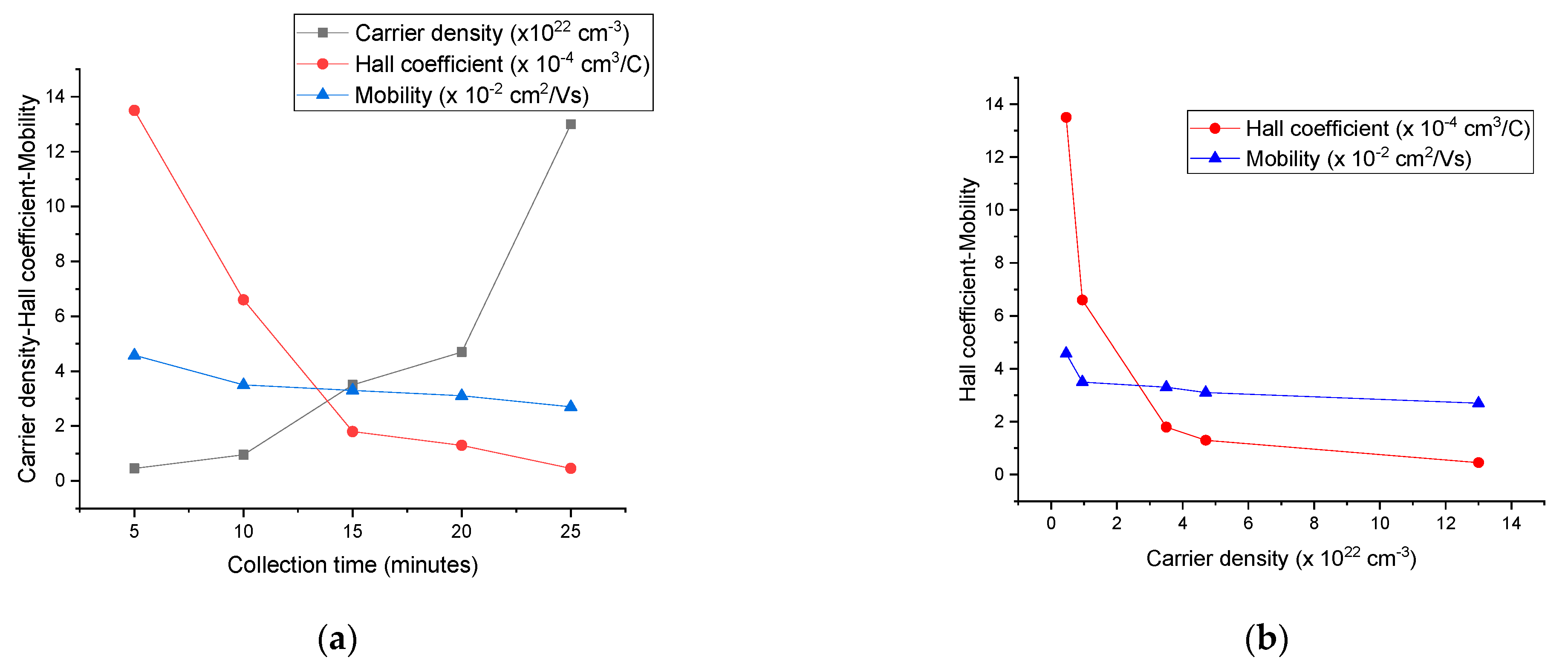
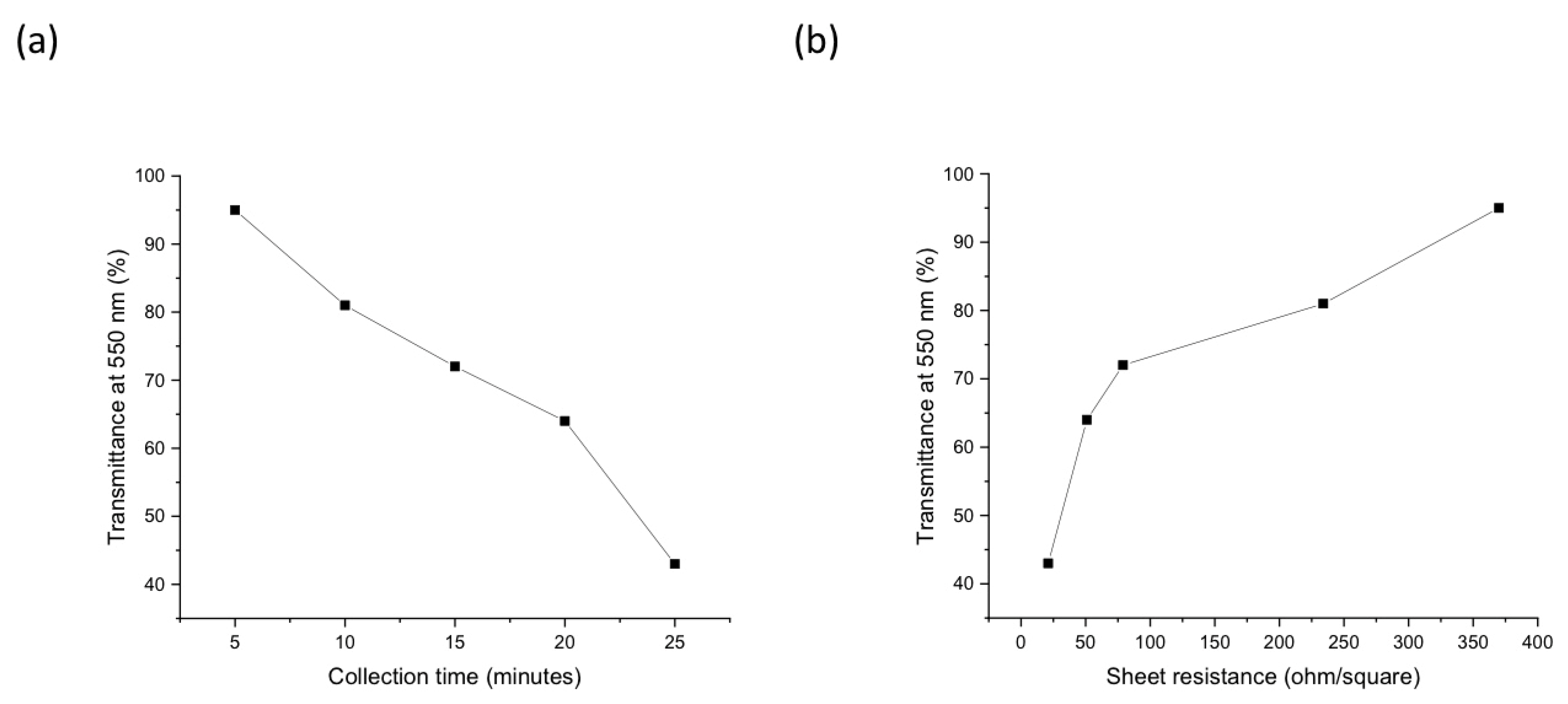
| Carrier Density (cm−3 ) | Mobility (cm2/Vs) | Hall Coefficient (cm3/C) | Carrier Type | Sheet Resistance (ohm/Square) | Collection Time (Minutes) |
|---|---|---|---|---|---|
| 4.6 × 10²¹ | 4.58 × 10⁻² | 1.35 × 10⁻³ | P-type | 370 | 5 |
| 9.5 × 10²¹ | 3.5 × 10⁻² | 6.6 × 10⁻⁴ | P-type | 234 | 10 |
| 3.5 × 10²² | 3.3 × 10⁻² | 1.8 × 10⁻⁴ | P-type | 79 | 15 |
| 4.7 × 10²² | 3.1 × 10⁻² | 1.3 × 10⁻⁴ | P-type | 51 | 20 |
| 1.3 × 10²³ | 2.7 × 10⁻² | 4.6 × 10⁻⁵ | P-type | 21 | 25 |
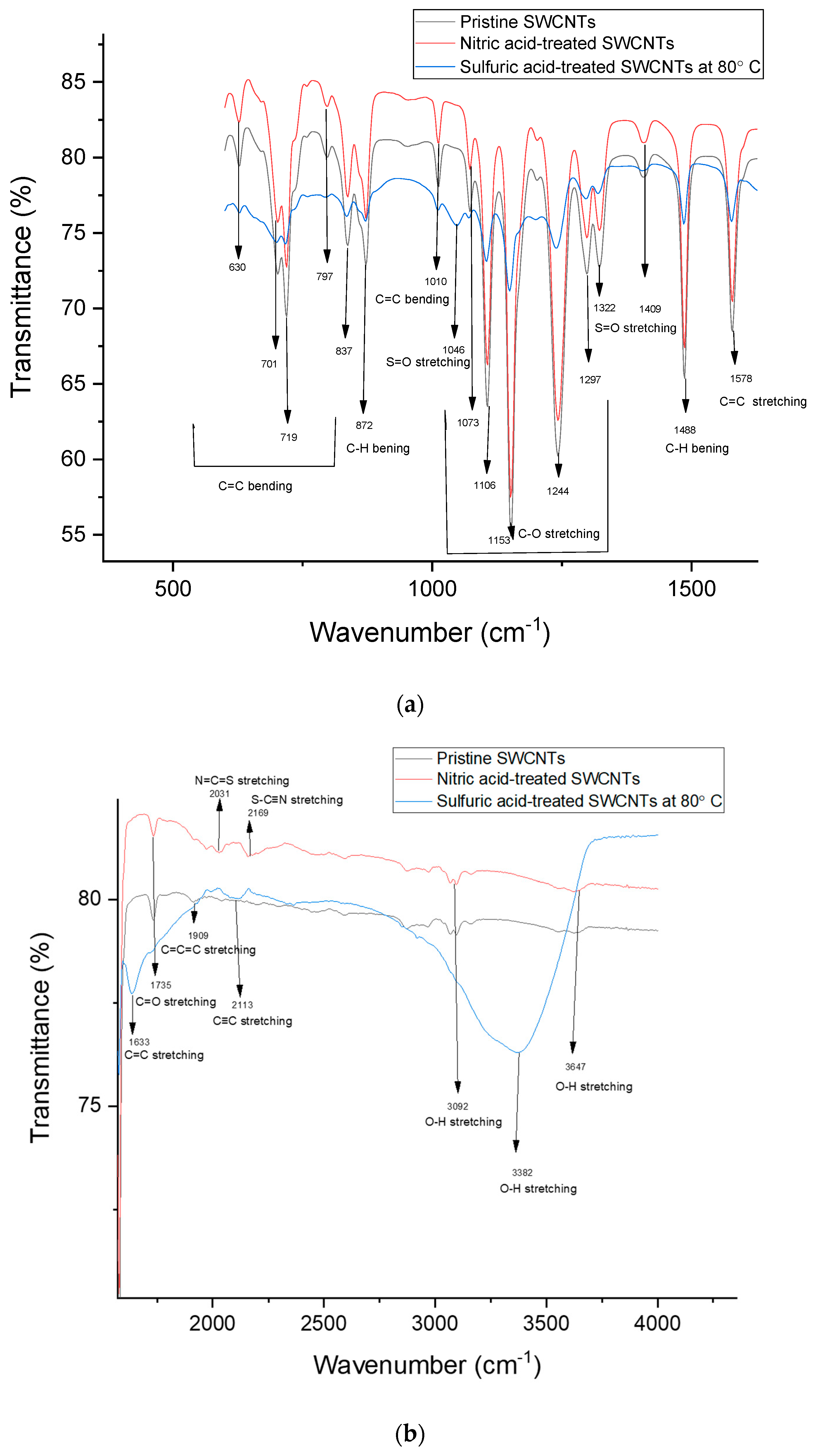
| Case | Acid Treatment | Carrier Density (cm−3) | Hole Mobility (cm2/Vs) | Hall Coefficient (cm3/C) | Carrier Type | Sheet Resistance (ohm/Square) | Conductivity (S/m) |
|---|---|---|---|---|---|---|---|
| A | 30 min H2SO4 (65 w/w %) treatment + DI water rinsing | 7.7 × 10²⁰ | 0.75 | 8 × 10⁻³ | P-type | 139 | 9240 |
| B | 30 min H2SO4 (65 w/w %) treatment at 80 °C + DI water rinsing | 3.2 × 10²⁰ | 1.5 | 2 × 0−2 | P-type | 163 | 7680 |
| C | 30 min H2SO4 (65 w/w %) treatment + DI water rinsing + ethanol rinsing | 8.4 × 10²¹ | 0.09 | 7.7 × 10⁻⁴ | P-type | 107 | 12,096 |
| D | 30 min H2SO4 treatment (4 M) + DI water rinsing | 5 × 10²¹ | 0.08 | 1.4 × 10⁻³ | P-type | 228 | 6400 |
| E | 30 min HCL treatment (4 M) + DI water rinsing | 8.8 × 10²¹ | 0.1 | 8.8 × 10⁻⁴ | P-type | 115 | 14,060 |
| F | 30 min HNO3 (4 M) + DI water rinsing | 1.2 × 10²² | 0.16 | 5.8 × 10⁻⁴ | P-type | 43 | 30,720 |
| G | Without treatment | 9.5 × 10²¹ | 0.035 | 6.6 × 10⁻⁴ | P-type | 243 | 5320 |
Disclaimer/Publisher’s Note: The statements, opinions and data contained in all publications are solely those of the individual author(s) and contributor(s) and not of MDPI and/or the editor(s). MDPI and/or the editor(s) disclaim responsibility for any injury to people or property resulting from any ideas, methods, instructions or products referred to in the content. |
© 2024 by the authors. Licensee MDPI, Basel, Switzerland. This article is an open access article distributed under the terms and conditions of the Creative Commons Attribution (CC BY) license (https://creativecommons.org/licenses/by/4.0/).
Share and Cite
Dolafi Rezaee, M.; Dahal, B.; Watt, J.; Abrar, M.; Hodges, D.R.; Li, W. Structural, Electrical, and Optical Properties of Single-Walled Carbon Nanotubes Synthesized through Floating Catalyst Chemical Vapor Deposition. Nanomaterials 2024, 14, 965. https://doi.org/10.3390/nano14110965
Dolafi Rezaee M, Dahal B, Watt J, Abrar M, Hodges DR, Li W. Structural, Electrical, and Optical Properties of Single-Walled Carbon Nanotubes Synthesized through Floating Catalyst Chemical Vapor Deposition. Nanomaterials. 2024; 14(11):965. https://doi.org/10.3390/nano14110965
Chicago/Turabian StyleDolafi Rezaee, Melorina, Biplav Dahal, John Watt, Mahir Abrar, Deidra R. Hodges, and Wenzhi Li. 2024. "Structural, Electrical, and Optical Properties of Single-Walled Carbon Nanotubes Synthesized through Floating Catalyst Chemical Vapor Deposition" Nanomaterials 14, no. 11: 965. https://doi.org/10.3390/nano14110965