Abstract
In this study, the effect of annealing and substrate conditions on the ferroelectricity of undoped hafnium oxide (HfO2) was analyzed. Hafnium oxide was deposited on various substrates such as platinum, titanium nitride, and silicon (Pt, TiN, Si) through RF magnetron sputtering. Annealing was performed in a nitrogen atmosphere at temperatures ranging from 400 to 600 °C, and the process lasted anywhere from 1 to 30 min. As a result, it was confirmed that the orthorhombic phase, the main cause of ferroelectricity, was dominant after a post-anneal at 600 °C for 30 min. Additionally, it was observed that interface mixing between hafnium oxide and the substrate may degrade ferroelectricity. Accordingly, the highest remanent polarization, measured at 14.24 μC/cm2, was observed with the Pt electrode. This finding was further corroborated by piezo force microscopy and endurance tests, with the results being significant compared to previously reported values. This analysis demonstrates that optimizing substrate and annealing conditions, rather than doping, can enhance the ferroelectricity of hafnium oxide, laying the foundation for the future development of ferroelectric-based transistors.
1. Introduction
Currently, commercially available memory is mainly divided into volatile and non-volatile memory, represented by dynamic random-access memory (DRAM) and NAND flash memory, respectively. DRAM operates at fast write and read speeds as it stores volatile memory, while NAND flash memory is a non-volatile memory operating at slower write and read speeds and with lower power efficiency. Therefore, various next-generation memories, combining the advantages of both types, are being studied. Among them, the most representative is ferroelectric memory [1,2,3]. This type of memory uses ferroelectric material, which spontaneously separates positive and negative charges without an external electrical stimulus. Ferroelectric memory is well-known for its faster operation speed compared to conventional memory, low power consumption, and applicability to non-volatile memory due to spontaneous polarization [4,5]. There are various ferroelectric materials, with perovskite-structured oxide being the first studied [6,7]. Perovskite oxide, characterized by an ABX3 crystal structure, has metal ions at the center of each unit cell. When an electric field is applied, the off-center motion of these metal ions causes spontaneous polarization, making this material initially significant in ferroelectric research [6,7]. However, applying thin perovskite oxide to state-of-the-art ferroelectric devices is challenging; its ferroelectricity degrades significantly at thicknesses below tens of nanometers [8,9], rendering complex perovskite oxide inadequate for scaling down to sub-nanometer dimensions of devices [10]. Therefore, identifying an alternative ferroelectric material to perovskite oxides is crucial. As a result, several ferroelectric materials for the two-component system have been proposed, including hafnium oxide [11,12,13,14,15,16]. Widely used in semiconductors, hafnium oxide is an insulator with a high dielectric constant and stable properties in thin films. Its characteristics vary depending on the crystal structure, which generally consists of monoclinic, tetragonal, and orthorhombic phases. Usually, the monoclinic and tetragonal structures typically exhibit dielectric properties. In contrast, the orthorhombic phase, with its non-centrosymmetric structure [11], allows for spontaneous polarization of the oxygen atoms in HfO2 when an electric field is applied, resulting in ferroelectricity. Various deposition and post-treatment methods have been explored to induce this orthorhombic phase. Atomic layer deposition (ALD) of HfO2 allows for thin film formation but struggles to induce the non-centrosymmetric orthorhombic phase due to limited process control variables and a stable chemical bonding mechanism. Studies have shown that reducing the thickness of ALD-deposited HfO2 films enhances their ferroelectricity [12]. However, this approach also increases the risk of dielectric breakdown and leakage current in the HfO2 films. And pulsed laser deposition (PLD) also hard to induce the ferroelectricity of HfO2 with any pre- and post-treatment, like annealing [13]. Consequently, the deposition of HfO2 using physical vapor deposition (PVD), particularly sputtering, is being considered as an alternative method.
Compared to atomic layer deposition (ALD), sputtering offers a faster deposition rate and provides various process variables, including gas type, RF power, and working pressure. Sputtering is advantageous for controlling defect concentration, which is crucial for inducing the orthorhombic phase [15]. Due to these advantages, numerous studies have focused on fabricating ferroelectric HfO2 through sputtering followed by post-annealing. However, post-annealing is necessary to induce ferroelectricity in HfO2 deposited by sputtering, requiring a high thermal budget. For instance, a remanent polarization (2Pr) of 12 μC/cm2 in HfO2 films is achieved after post-annealing at 1000 °C [12]. Because of these problems, co-sputtering has emerged. Co-sputtering requires a low thermal budget to induce ferroelectricity, but remanent polarization was likewise lower than that of HfO2 deposited by ALD. This is the reason for the limit on the use of ferroelectric HfO2 in advanced integrated circuit (IC) manufacturing due to its optimization with restricted thermal budgets [14].
In this study, HfO2 was deposited on metal substrates such as Pt and TiN, as well as on a Si substrate, using RF sputtering and then annealed by rapid thermal annealing (RTA). The electrical and ferroelectric properties of the HfO2 film were analyzed using a positive-up-negative-down (PUND) test, polarization hysteresis curve, piezo force microscopy (PFM), conductive atomic force microscopy (c-AFM), and endurance tests. As a result, the impact of substrate types and annealing conditions on optimizing ferroelectric properties was determined. The remanent polarization of HfO2 deposited on a Pt substrate and annealed at 600 °C for 30 min was measured at 14.24 μC/cm2, meeting the low thermal budget requirements for ferroelectricity [15]. Additionally, various analyses, including grazing incidence X-ray diffraction (GIXRD), transmission electron microscopy (TEM), and X-ray photoelectron spectroscopy (XPS), were conducted to understand the effects of fabrication process conditions on the ferroelectric characteristics of HfO2 thin films. These analyses confirmed that the Pt substrate had more oxygen vacancies associated with the orthorhombic phase of HfO2 and exhibited less interface mixing between the substrate and the HfO2 film. Ultimately, this study provides valuable insights into optimizing ferroelectric HfO2 for compatibility with conventional semiconductor devices, which could significantly impact the development of future ferroelectric devices.
2. Materials and Methods
First, 100 nm Pt and TiN were deposited on a 4-inch SiO2 substrate by e-beam evaporation and the radio frequency magnetron sputtering technique. And then, 15 nm HfO2 films were deposited on a Pt, TiN, low-resistive (1 × 10⁻³ Ω cm) p-Si substrate in a large area (2 in.) by radio frequency magnetron sputtering technique (Scientific Eng & Tech, Suwon, Republic of Korea). An ultrapure commercially available 2-inch hafnium oxide target (HfO2, 99.999%, VTM, Incheon, Republic of Korea) was used to grow the thin films. The distance between the target and the substrate holder is 40 cm. The sputtering was performed with 100 W of rf power and a working pressure of 2 mTorr. Ultrapure argon gas with a flow rate of 30 sccm and oxygen gas with a flow rate of 10 sccm were used to maintain the working pressure. Following the HfO2 deposition at room temperature, the rapid thermal annealing (Real RTP-100, Daegu, Republic of Korea) was performed under a nitrogen atmosphere with a flow rate of 30 sccm at 400~600 °C for 1~30 min, which led to the formation of the crystalline HfO2. Finally, 50-nm-thick top Pt/Au electrodes were deposited by an E-beam evaporator using a Pt/Au source (99.99%, TFN, Seoul, Republic of Korea). The crystalline nature of HfO2 was studied by grazing incidence X-ray diffraction (Ultima III, Rigaku, Tokyo, Japan). The piezo force microscopy (PFM) and conductive atomic force microscopy (c-AFM) measurements were performed by atomic force microscopy (MFP-3D, Oxford Instruments, Abingdon, UK) with a Pt/Ir-coated Si probe (AC240TM) probe. The PFM measurement was carried out by the PFM technique with an AC signal of 3 V/71 kHz. The c-AFM measurement was carried out by the c-AFM technique with a DC signal of 1 V. The P-V hysteresis curve and positive-up-negative-down (PUND) test measurements were performed by a probe station (SCS-4200, Keithley, Cleveland, OH, USA). The compositional analysis of HfO2 films was carried out using X-ray photoelectron spectroscopy (K-Alpha+, Thermo Fisher Scientific, Waltham, MA, USA).
3. Results
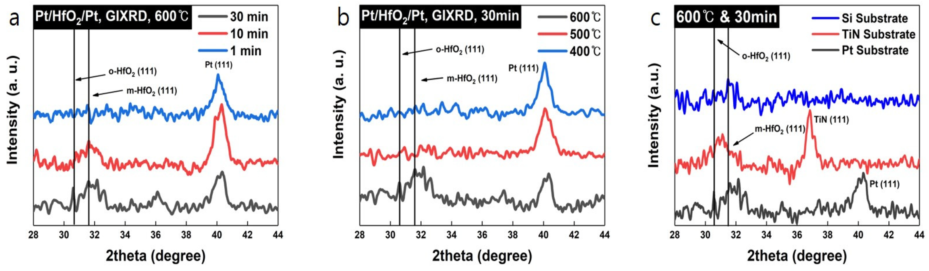
Initially, the crystal structure of the HfO2 thin film, as influenced by the substrate type, annealing temperature, and time, was analyzed using grazing incidence X-ray diffraction (GIXRD). Figure 1a shows the GIXRD data obtained after depositing HfO2 on a Pt substrate and annealing it for different durations at 600 °C. In Figure 1a, peaks at 2θ = 30.33° and 31.44° were identified, corresponding to the orthorhombic and monoclinic phases of HfO2 [17]. The peak at 2θ = 39.82° corresponds to Pt (111) [18,19]. Additionally, an increase in the intensity of the orthorhombic phase peak was observed with longer annealing times. Figure 1b presents the GIXRD data for HfO2 deposited on a Pt substrate and annealed at various temperatures for 30 min, demonstrating that higher temperatures strengthen HfO2 crystallization. Based on these findings, HfO2 was deposited on Pt, TiN, and Si substrates and then annealed at 600 °C for 30 min, with the results evaluated by GIXRD. As shown in Figure 1c, HfO2 deposited on Si formed the dominant monoclinic phase. However, when deposited on TiN and Pt, a mixture of orthorhombic and monoclinic phases was observed. We anticipated that different lattice parameters of the substrate crystal phase could affect the HfO2 film phase. Also, the orthorhombic peak of HfO2 can overlap with tetragonal or other non-ferroelectric phases [20]. Therefore, the impact of the substrate on the crystallinity and ferroelectricity of HfO2, even when deposited under the same conditions, is significant, highlighting the importance of interface-controlled growth for optimizing HfO2 ferroelectricity.
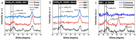
Figure 1.
GIXRD data for (a) different annealing times, (b) different temperatures, and (c) different substrates with 1.5° of incidence.
The PUND test was initially conducted to assess the relationship between crystallinity and ferroelectricity in these thin films. As observed in Figure S3, the current in the first pulse is higher than in the second, which is attributed to the initial current required for polarization, thus confirming the ferroelectricity of the HfO2 film [21]. Figure S3 also shows the results of the PUND test on a Pt/HfO2/Pt structure device annealed at 600 °C for 30 min. It was observed that with each pulse, the difference in measured current increased.
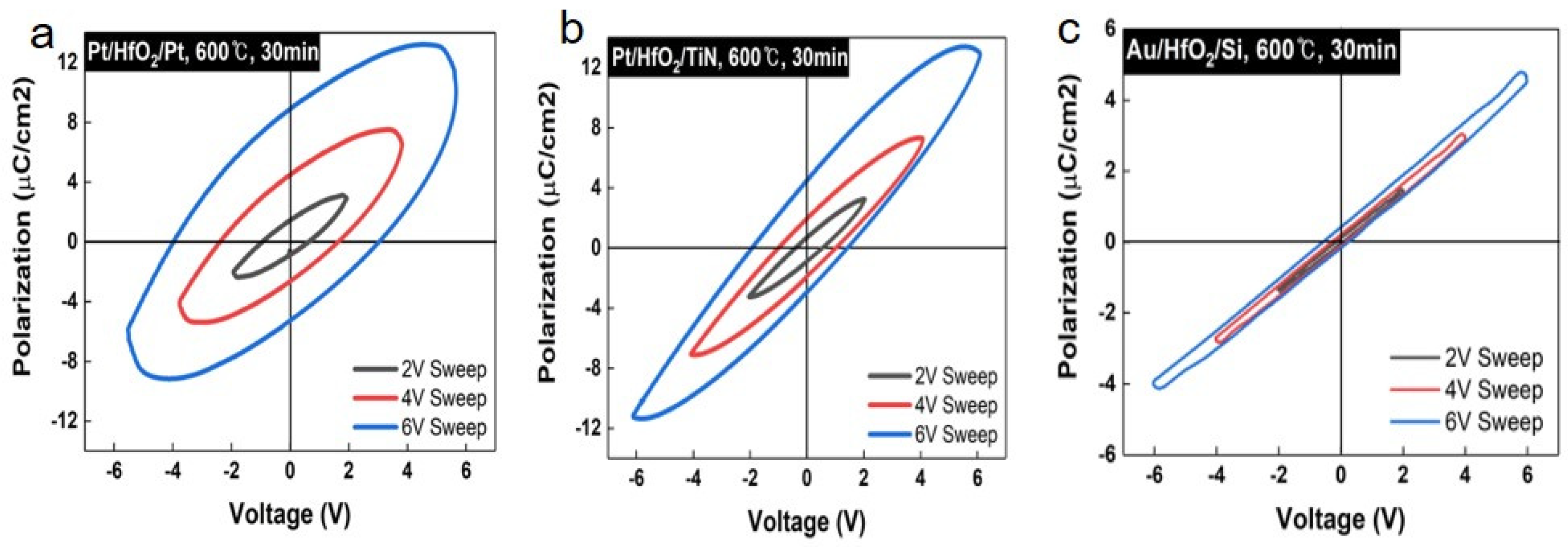
The polarization current rose with an increasing pulse voltage. Furthermore, the remanent polarization of each device under identical annealing conditions was measured. Another voltage pulse model, shown in Figure 2a, was used to plot the polarization curve for HfO2 films deposited on each substrate and annealed at 600 °C for 30 min. The polarization curves of the HfO2 films linearly varied in the order of Pt, TiN, and Si substrates (Figure 2a,c). Similarly, the remanent polarization and coercive field at a 6 V sweep decreased in the order of Pt, TiN, and Si substrates, as shown in Table 1 and Figure S4. Additionally, for the Si substrate, the polarization loop hysteresis was notably smaller compared to other devices, which correlates with the absence of orthorhombic-phase HfO2, as demonstrated in the XRD data (Figure 1c), due to the lack of initial crystallization on the amorphous SiO2 on Si. To further explore the physicochemical relationship between the orthorhombic phase of HfO2 and the substrate, transmission electron microscopy (TEM) analysis and X-ray photoelectron spectroscopy (XPS) studies were conducted.
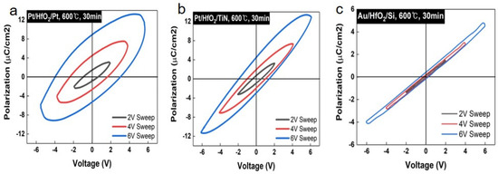
Figure 2.
P-V hysteresis curves for HfO2 deposited on (a) Pt, (b) TiN, and (c) Si substrate.

Table 1.
In 6V voltage-sweeping remanent polarization (2Pr) and absolute coercive field (Ec) data of HfO2 film deposited on Pt, TiN, and Si substrates after annealing at 600 °C for 30 min.
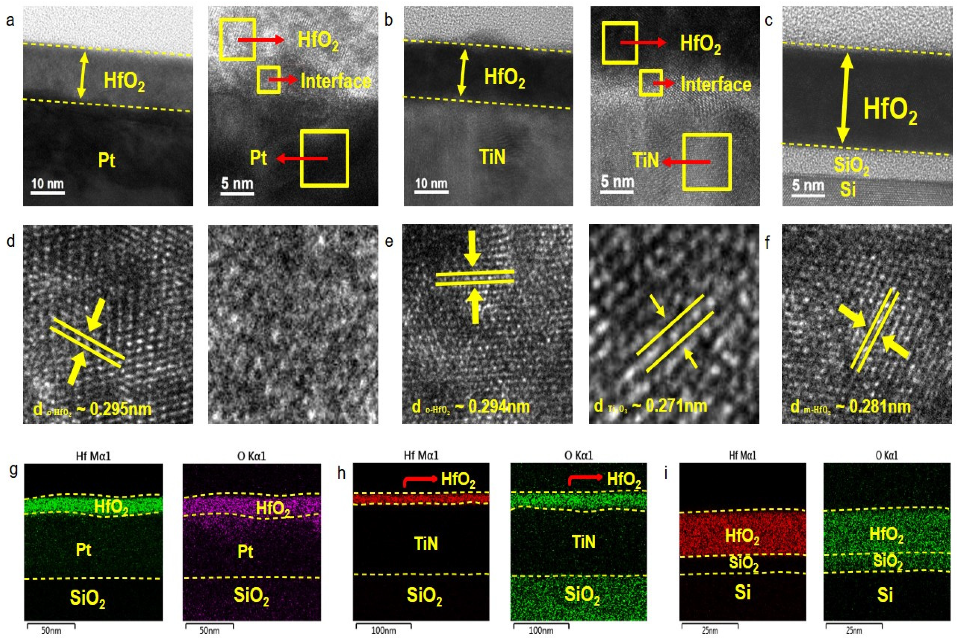
The structure of HfO2 annealed on each substrate was analyzed using cross-sectional transmission electron microscopy (TEM). The thickness of the HfO2 film was consistently ~15 nm for all samples. Initially, on the Pt substrate, local chemical mixing at the interface between HfO2 and Pt was observed, with the amorphous structure of this interface confirmed by TEM imaging. In the bulk HfO2 film, the orthorhombic phase was identified, with an interplanar spacing of 0.295 nm, matching the (111) orthorhombic HfO2 phase [22,23]. Figure 3g showed oxygen atom diffusion beyond the HfO2 layer into the topmost part of the Pt electrode, leading to the partial generation of oxygen vacancies in HfO2, as evidenced in the supporting information (Figure S1). For the TiN substrate, the (111) orthorhombic phase of bulk HfO2, with the same interplanar spacing as the Pt substrate, was confirmed. However, the interface displayed a clear crystal structure between HfO2 and TiN. The measured interplanar distance at the interface was 0.271 nm, consistent with Ti2O3 [24]. Figure 3h revealed a wider distribution of oxygen atoms compared to Hf atoms in the HfO2 film, indicating interface mixing between the HfO2 film and TiN substrate, corroborated by the presence of Ti2O3 as identified in TEM analysis. In contrast, when HfO2 was deposited on the Si substrate, unlike in the other cases, interface mixing was not observed (see Figure 3c,i). The bulk HfO2 demonstrated a clear crystal structure with an interplanar spacing of 0.281 nm, corresponding to monoclinic HfO2 and aligning with the GIXRD results (see Figure 1c) [25]. TEM-EDS images confirmed that the substrate influences the bulk and interface crystal structures of HfO2 after annealing. Notably, while bulk HfO2 films on Pt and TiN substrates were primarily in the orthorhombic phase, the remanent polarization values differed by about threefold.
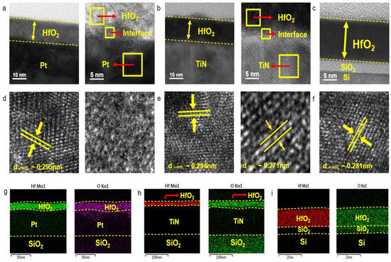
Figure 3.
The low-resolution TEM images of the film were deposited on (a) Pt, (b) TiN and (c) Si and annealed at 600 °C for 30 min. The high-resolution TEM images of bulk HfO2 and interface between film and electrode deposited on (d) Pt, (e) TiN, and (f) Si. TEM-EDS elemental mapping images of HfO2 film deposited on (g) Pt, (h) TiN, and (i) Si.
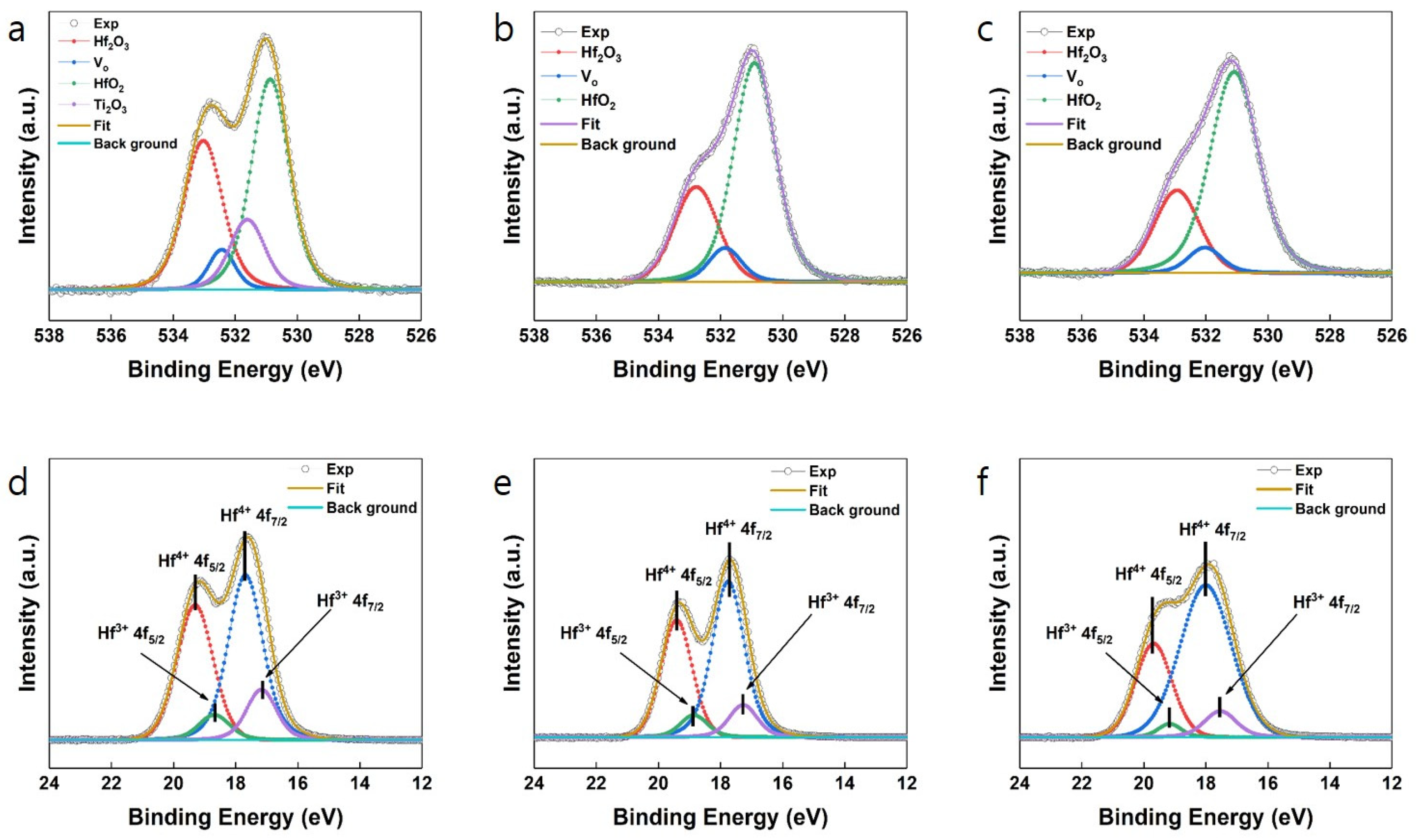
X-ray photoelectron spectroscopy (XPS) analysis was conducted to investigate the bonds and defects in HfO2, providing further evidence for the origin of different polarization properties. Figure 4 presents the O 1s and Hf 4f binding energy spectra of HfO2 deposited on each substrate. The O 1s spectra reveal the presence of oxygen vacancies and sub-hafnium oxide (Hf2O3 or Hf3+), with peak area fractions ranging from 24 to 33%. Notably, the subpeak corresponding to Ti2O3 at 531.61 eV was identified in HfO2 deposited on a TiN substrate. This finding suggests the formation of Ti2O3 (even with partial crystallization) at the interface between TiN and HfO2, as shown in Figure 3e, resulting from oxygen supply to TiN during HfO2 deposition. In the Hf 4f spectra, the presence of both Hf4+ and Hf3+ binding energy peaks was observed in all samples, aligning with the subphase O species bound to Hf4+ and Hf3+ in the O 1s spectra. The increased amount of Hf3+, indicative of oxygen vacancy formation, is attributed to the reduction of HfO2 during post-deposition annealing in an N2 gas ambience.
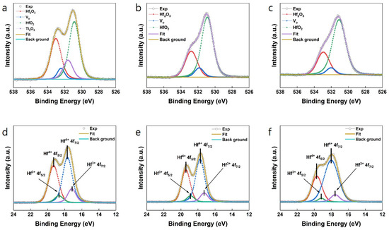
Figure 4.
O 1s spectra for HfO2 deposited on (a) Pt, (b) TiN, and (c) Si. Hf 4f spectra for HfO2 deposited on (d) Pt, (e) TiN, and (f) Si.
Table 2 summarizes the binding energy positions and relative bonding ratios from the O 1s spectra. The main peaks for all samples are positioned between 531.08 eV and 530.87 eV, corresponding to HfO2 [26,27,28,29,30] (Figure 4a–c). Various dominant peaks were observed at 531.85 eV, 532.43 eV, and 532.03 eV, corresponding to oxygen vacancies on different substrates. Additionally, peaks at 532.78 eV, 533.02 eV, and 532.93 eV correspond to Hf2O3, and a peak at 531.61 eV corresponds to Ti2O3, varying with the substrate [26,27,28,29,30]. The oxygen bonding ratio was quantitatively calculated from the XPS of the O 1s spectra, revealing that in all samples, the HfO2 bonding ratio was the highest, followed by Hf2O3 and oxygen vacancies. Specifically, in the case of TiN, the HfO2 bonding ratio was lower due to Ti2O3. Additionally, the oxygen vacancy ratio was highest in the order of Pt, TiN, and Si. The previous crystal structure and remanent polarization value analyses (see Figure 1 and Figure 2) confirmed that HfO2′s ferroelectricity is significantly influenced by oxygen vacancies. Moreover, the interface between the substrate and HfO2 also impacts ferroelectricity, as seen in Figure 3c, where the native SiO2 layer on a Si substrate may hinder the initial spontaneous polarization of ferroelectric HfO2. Table 2 shows that the oxygen vacancy ratio is very similar between Si and TiN substrates, yet the remanent polarization is about 5.5 times higher with the TiN substrate. Comparing the Pt and TiN substrates, a higher oxygen vacancy ratio was observed after annealing HfO2 on the Pt substrate, accompanied by localized interface mixing with its amorphous crystal structure. Since Pt is less reactive, interface mixing and crystallization are less likely to occur, unlike TiN, which is more susceptible to oxidation, leading to interface mixing and the crystallization of Ti2O3. Ti2O3, having much higher resistivity than Pt, acts as an insulator similar to SiO2. Also, oxygen migration by annealing can induce the metastable orthorhombic phase of the HfO2 film. Overall, these findings indicate that interfacial properties significantly affect ferroelectricity.
Table 2.
Binding energy and relative bond fraction in the O 1s spectra of HfO2 deposited on different substrates.
Furthermore, Table 3 provides information about binding energy positions and relative bonding ratios from the Hf 4f spectra. The main doublets of Hf4+ 4f5/2–Hf4+ 4f7/2 and two sub-doublets of Hf3+ 4f5/2–Hf3+ 4f7/2 were identified. The Hf4+ 4f5/2 peaks around 19.34 to 19.57 eV, separated by 1.6 eV from the Hf4+ 4f7/2 peak at 17.74 to 17.94 eV, originating from stoichiometric HfO2 [31,32,33]. The Hf3+ 4f5/2 peaks around 18.76 to 18.98 eV, separated by 1.6 eV from the Hf3+ 4f7/2 peak at 17.14 to 17.34 eV, are indicative of HfOx (x < 2) [33]. Table 2 and Table 3 confirm that the bonding ratios of HfO2 and Hf2O3 align with the calculated results from the O 1s and Hf 4f XPS spectra, allowing for analysis of the relationship between HfO2′s ferroelectricity and its atomic bonding structure through XPS analysis.
Table 3.
Binding energy and relative bond fraction in Hf 4f spectra of HfO2 deposited on different substrates.
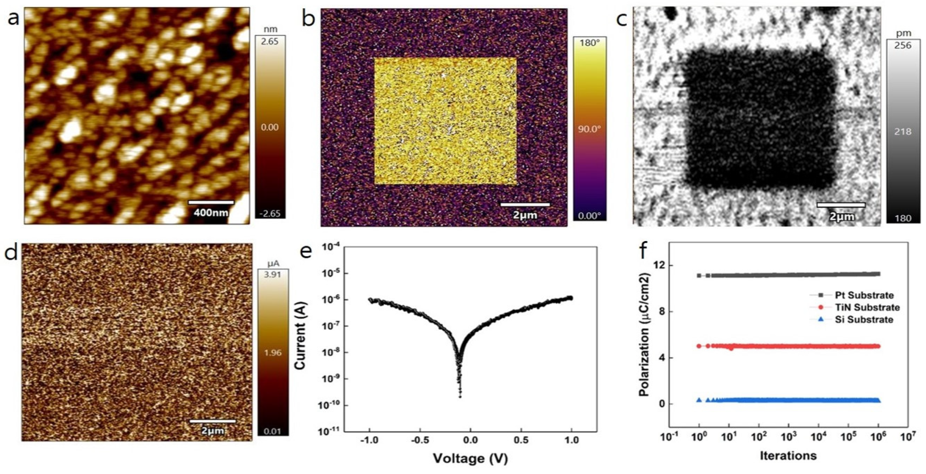
In Figure 5, the physical characteristics of HfO2, aimed at its suitability for nanoscale ferroelectric devices, were analyzed using atomic force microscopy (AFM), piezo force microscopy (PFM), and conductive atomic force microscopy (c-AFM). Additionally, an endurance test for polarization was conducted. Figure 5a presents an AFM image showing the surface roughness of HfO2 deposited on Pt, scanned over a 2 × 2 μm2 area. The root mean square (RMS) roughness, calculated from the AFM data, was 1.261 nm. Given that the average thickness of HfO2 is 15 nm, this indicates a relatively low surface roughness, even for films deposited by RF sputtering. The ferroelectricity of the HfO2 surface was then assessed with PFM. As depicted in Figure 5b,c, a 10 × 10 μm2 area was initially scanned without applying a bias to the probe tip. And then a 6 × 6 μm2 area was scanned by applying a +3 V bias to confirm the phase change. Because polarization direction is expressed by the color in the scale bar near the PFM image, phase change can be confirmed by the color of the scanned area. This resulted in a 180° phase change, indicating a complete reversal in the polarization direction of the surface, thereby confirming the potential of HfO2 in ferroelectric devices due to its effective polarization-switching capabilities [12,17,34]. Lastly, the I-V characteristics were measured using c-AFM. Figure 5d illustrates c-AFM scanning over a 10 × 10 μm2 area with a +1 V tip bias.
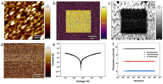
Figure 5.
(a) AFM image of the film surface, (b) PFM phase image with tip bias, (c) PFM amplitude image with tip bias, and (d) c-AFM image with tip bias of HfO2 deposited on Pt substrate. (e) local I-V measured by c-AFM, and (f) endurance test for HfO2 film deposited on each substrate.
We confirmed the leakage current map at the level of the μA scale in the corresponding image. As a result of calculating the average scanning current based on the data of the corresponding image, 1.97 μA was obtained, and the leakage current for 1 V sweeping at a specific point, the μA level of current was also confirmed (Figure 5e). Finally, the endurance test of HfO2 was conducted for each substrate. First, the charge is measured for each positive and negative pulse based on the voltage pulse model of the PUND test (Figure S3a). Next, the measured charge was calculated to obtain remanent polarization per 1 cycle, and then it was measured for each cycle. As a result, it was confirmed that the remanent polarization was maintained even after repeating 1 million cycles in all samples without noticeable degradation of polarization (Figure 5f). In addition, the magnitude of the remanent polarization depending on the substrate kind coincides with that in the P-V hysteresis data. As a result, the applicability of HfO2 to the ferroelectric device could be confirmed in various ways through a series of experiments, as described above.
4. Conclusions
We have deposited the ferroelectric HfO2 thin film on various substrates using RF magnetron sputtering and post-anneal-induced crystallization. The ferroelectric characteristics were revealed by P-V hysteresis, PUND measurement, and local piezo force microscopy. The in-depth atomic structure and crystal analysis were performed by TEM, XPS, and GIXRD. The orthorhombic phase revealed the ferroelectricity of HfO2 was dominant at 600 °C and the 30-min annealing condition was confirmed by GIXRD. Based on this result, the ferroelectricity of HfO2 annealed at 600 °C, and 30 min was confirmed through the PUND test. The remanent polarization of HfO2 was higher in the case of Pt (14.24 μC/cm2) than in other substrates (TiN, Si) at the same annealing condition. As a result of TEM, the orthorhombic phase of HfO2 deposited on Pt and TiN substrate was confirmed, but the monoclinic phase of HfO2 deposited on Si was confirmed, and this was similar to the result of GIXRD. In addition, TEM analysis revealed that when HfO2 was deposited on each substrate, local chemical mixing occurred at the interface between HfO2 and substrate, and then the HfO2 phase was different depending on the substrates. The mixed phase of HfO2 showed the inferior initial spontaneous polarization of ferroelectric HfO2. From XPS measurements, the oxygen vacancy was highest in the order of Pt, TiN, and Si substrates. The orthorhombic phase of HfO2 leading to the relatively higher oxygen vacancy was manifested by GIXRD and TEM. The overall observation of the data suggests that the initial growth of HfO2 film was considerably affected by the different substrate effects to split its phase either orthorhombic-dominant or monoclinic-dominant, which is directly correlated to the degree of oxygen vacancy formation. This study therefore represents not only a process control and mechanism for ultra-thin ferroelectric HfO2 films requiring a low thermal budget to anneal, but also a cornerstone for applications including polarization-based memory and ferroelectric-based transistors.
Supplementary Materials
The following supporting information can be downloaded at: https://www.mdpi.com/article/10.3390/nano14171386/s1, Figure S1. The method of electrical and ferroelectric properties measurement. Figure S2. TEM-EDS data. (a,b,c) EDS-area & line data of Pt, TiN, Si substrate for each element and atomic percent. Figure S3. PUND test and Polarization current for Pt/HfO2/Pt device after annealed 600 °C and 30 min. (a) Bias pulse wave setup for PUND test. (b) Current vs. pulse time plot of PUND test for Pt/HfO2/Pt device after annealed 600 °C for 30 min. Figure S4. Ferroelectric Properties for each device (a) Bias pulse wave setup for drawing polarization curve. (b) Remanent polarization (2Pr) and (c) coercive field (Ec) data of HfO2 film deposited on Pt, TiN, Si substrate at 6 V sweeping. Figure S5. FFT images The low-resolution FFT images of local point in bulk HfO2 film deposited on (a) Pt, (b) TiN, (c) Si and annealed at 600 °C for 30 min. Figure S6. I–V Curve Representative switching current of HfO2 film deposited on Pt Substrate and annealed at 600 °C for 30 min. Table S1. XPS information for HfO2 film deposited on Pt, TiN, Si and annealed at 600 °C for 30 min.
Author Contributions
Conceptualization, S.L. (Seokwon Lim), M.K. and H.S.; Data curation, S.L. (Seokwon Lim), Y.A., B.W., H.P. and S.L. (Suwan Lee); Formal analysis, S.L. (Seokwon Lim), Y.A., B.W., H.P. and S.L. (Suwan Lee); Funding acquisition, H.S.; Methodology, S.L. (Seokwon Lim) and H.S.; Project administration, M.K. and H.S.; Supervision, M.K. and H.S.; Writing—original draft, S.L. (Seokwon Lim); Writing—review and editing, B.W., S.L. (Suwan Lee) and H.S. All authors have read and agreed to the published version of the manuscript.
Funding
Hyungtak Seo reports financial support was provided by the National Research Foundation of Korea.
Data Availability Statement
Data are contained within the article and supporting information.
Acknowledgments
This study was supported through the National Research Foundation of Korea [RS-2024-00336428, RS-2024-00403069 and NRF-2022M3I7A3037878] of the Ministry of Science and ICT, Republic of Korea and Korea Evaluation Institute of Industrial Technology (Project No: (20022717) funded by Ministry of Trade, Industry and Energy, Republic of Korea.
Conflicts of Interest
The authors declare no conflicts of interest.
References
- Wu, S.-Y. A new ferroelectric memory device, metal-ferroelectric-semiconductor transistor. IEEE Trans. Electron Devices 1974, 21, 499–504. [Google Scholar] [CrossRef]
- Vorotilov, K.A.; Sigov, A.S. Ferroelectric memory. Phys. Solid State. 2012, 54, 894–899. [Google Scholar] [CrossRef]
- Lue, H.-T.; Wu, C.-J.; Tseng, T.-Y. Device modeling of ferroelectric memory field-effect transistor for the application of ferroelectric random access memory. IEEE Trans. Ultrason. Ferroelectr. Freq. Control. 2003, 50, 5–14. [Google Scholar] [CrossRef]
- Müller, J.; Polakowski, P.; Mueller, S.; Mikolajick, T. Ferroelectric Hafnium Oxide Based Materials and Devices: Assessment of Current Status and Future Prospects. ECS J. Solid State Sci. Technol. 2015, 4, N30. [Google Scholar] [CrossRef]
- Mikolajick, T.; Schroeder, U.; Slesazeck, S. The Past, the Present, and the Future of Ferroelectric Memories. IEEE Trans. Electron Devices 2020, 67, 1434–1443. [Google Scholar] [CrossRef]
- Rørvik, P.M.; Grande, T.; Einarsrud, M.-A. One-Dimensional Nanostructures of Ferroelectric Perovskites. Adv. Mater. 2011, 23, 4007–4034. [Google Scholar] [CrossRef] [PubMed]
- Pan, Q.; Liu, Z.-B.; Tang, Y.-Y.; Li, P.-F.; Ma, R.-W.; Wei, R.-Y.; Zhang, Y.; You, Y.-M.; Ye, H.-Y.; Xiong, R.-G. A Three-Dimensional Molecular Perovskite Ferroelectric: (3-Ammoniopyrrolidinium)RbBr3. J. Am. Chem. Soc. 2017, 139, 3954–3957. [Google Scholar] [CrossRef]
- Ihlefeld, J.F.; Harris, D.T.; Keech, R.; Jones, J.L.; Maria, J.-P.; Trolier-McKinstry, S. Scaling Effects in Perovskite Ferroelectrics: Fundamental Limits and Process-Structure-Property Relations. J. Am. Ceram. Soc. 2016, 99, 2537–2557. [Google Scholar] [CrossRef]
- Park, M.H.; Lee, Y.H.; Mikolajick, T.; Schroeder, U.; Hwang, C.S. Review and perspective on ferroelectric HfO2-based thin films for memory applications. MRS Commun. 2018, 8, 795–808. [Google Scholar] [CrossRef]
- Park, J.Y.; Lee, D.H.; Park, G.H.; Lee, J.; Lee, Y.; Park, M.H. A perspective on the physical scaling down of hafnia-based ferroelectrics. Nanotechnology 2023, 34, 202001. [Google Scholar] [CrossRef]
- Fan, Z.; Chen, J.; Wang, J. Ferroelectric HfO2-based materials for next-generation ferroelectric memories. J. Adv. Dielect. 2016, 6, 1630003. [Google Scholar] [CrossRef]
- Polakowski, P.; Müller, J. Ferroelectricity in undoped hafnium oxide. Appl. Phys. Lett. 2015, 106, 232905. [Google Scholar] [CrossRef]
- Shimizu, T.; Katayama, K.; Kiguchi, T.; Akama, A.; Konno, T.J.; Funakubo, H. Growth of epitaxial orthorhombic YO1.5-substituted HfO2 thin film. Appl. Phys. Lett. 2015, 107, 032910. [Google Scholar] [CrossRef]
- Hsain, H.A.; Lee, Y.; Materano, M.; Mittmann, T.; Payne, A.; Mikolajick, T.; Schroeder, U.; Parsons, G.N.; Jones, J.L. Many routes to ferroelectric HfO2: A review of current deposition methods. J. Vac. Sci. Technol. A 2022, 40, 010803. [Google Scholar] [CrossRef]
- Mittmann, T.; Materano, M.; Lomenzo, P.D.; Park, M.H.; Stolichnov, I.; Cavalieri, M.; Zhou, C.; Chung, C.-C.; Jones, J.L.; Szyjka, T.; et al. Origin of Ferroelectric Phase in Undoped HfO2 Films Deposited by Sputtering. Adv. Mater. Interfaces 2019, 6, 1900042. [Google Scholar] [CrossRef]
- Luo, Y.; Tang, Z.; Yin, X.; Chen, C.; Fan, Z.; Qin, M.; Zeng, M.; Zhou, G.; Gao, X.; Lu, X. Ferroelectricity in dopant-free HfO2 thin films prepared by pulsed laser deposition. J. Mater. 2022, 8, 311–318. [Google Scholar] [CrossRef]
- Kumar, M.; Seo, H. High-Performing Self-Powered Photosensing and Reconfigurable Pyro-photoelectric Memory with Ferroelectric Hafnium Oxide. Adv. Mater. 2022, 34, 2106881. [Google Scholar] [CrossRef]
- Li, W.; Sun, Z.; Tian, D.; Nevirkovets, I.P.; Dou, S.-X. Platinum dendritic nanoparticles with magnetic behavior. J. Appl. Phys. 2014, 116, 033911. [Google Scholar] [CrossRef]
- Panomsuwan, G.; Takai, O.; Saito, N. Epitaxial growth of (111)-oriented BaTiO3/SrTiO3 perovskite superlattices on Pt(111)/Ti/Al2O3(0001) substrates. Appl. Phys. Lett. 2013, 103, 112902. [Google Scholar] [CrossRef]
- Song, T.; Tan, H.; Dix, N.; Moalla, R.; Lyu, J.; Saint-Girons, G.; Bachelet, R.; Sánchez, F.; Fina, I. Stabilization of the Ferroelectric Phase in Epitaxial Hf1–xZrxO2 Enabling Coexistence of Ferroelectric and Enhanced Piezoelectric Properties. ACS Appl. Electron. Mater. 2021, 3, 5, 2106–2113. [Google Scholar] [CrossRef]
- Ryu, H.; Xu, K.; Kim, J.; Kang, S.; Guo, J.; Zhu, W. Exploring New Metal Electrodes for Ferroelectric Aluminum-Doped Hafnium Oxide. IEEE Trans. Electron Devices 2019, 66, 2359–2364. [Google Scholar] [CrossRef]
- Weeks, S.L.; Pal, A.; Narasimhan, V.K.; Littau, K.A.; Chiang, T. Engineering of Ferroelectric HfO2–ZrO2 Nanolaminates. ACS Appl. Mater. Interfaces 2017, 9, 13440–13447. [Google Scholar] [CrossRef]
- Lowther, J.E.; Dewhurst, J.K.; Leger, J.M.; Haines, J. Relative stability of ZrO2 and HfO2 structural phases. Phys. Rev. B 1999, 60, 14485–14488. [Google Scholar] [CrossRef]
- Ma, C.; Rossman, G.R. Tistarite, Ti2O3, a new refractory mineral from the Allende meteorite. Am. Mineral. 2009, 94, 841–844. [Google Scholar] [CrossRef]
- Robertson, A.L.; Solá, F.; Zhu, D.; Salem, J.; White, K.W. White, Microscale fracture mechanisms of HfO2-Si environmental barrier coatings. J. Eur. Ceram. Soc. 2019, 39, 2409–2418. [Google Scholar] [CrossRef]
- He, G.; Liu, M.; Zhu, L.Q.; Chang, M.; Fang, Q.; Zhang, L.D. Effect of postdeposition annealing on the thermal stability and structural characteristics of sputtered HfO2 films on Si (100). Surf. Sci. 2005, 576, 67–75. [Google Scholar] [CrossRef]
- Hernández-Arriaga, H.; López-Luna, E.; Martínez-Guerra, E.; Turrubiartes, M.M.; Rodríguez, A.G.; Vidal, M.A. Growth of HfO2/TiO2 nanolaminates by atomic layer deposition and HfO2-TiO2 by atomic partial layer deposition. J. Appl. Phys. 2017, 121, 064302. [Google Scholar] [CrossRef]
- Wang, Z.; Mao, X.; Chen, P.; Xiao, M.; Monny, S.A.; Wang, S.; Konarova, M.; Du, A.; Wang, L. Understanding the Roles of Oxygen Vacancies in Hematite-Based Photoelectrochemical Processes. Angew. Chem. 2019, 131, 1042–1046. [Google Scholar] [CrossRef]
- Kumar, M.; Mookerjee, S.; Som, T. Field-induced doping-mediated tunability in work function of Al-doped ZnO: Kelvin probe force microscopy and first-principle theory. Nanotechnology 2016, 27, 375702. [Google Scholar] [CrossRef]
- Basu, T.; Kumar, M.; Nandy, S.; Satpati, B.; Saini, C.P.; Kanjilal, A.; Som, T. Thickness-dependent blue shift in the excitonic peak of conformally grown ZnO: Al on ion-beam fabricated self-organized Si ripples. J. Appl. Phys. 2015, 118, 04903. [Google Scholar] [CrossRef]
- Zhang, R.; Huang, H.; Xia, Q.; Ye, C.; Wei, X.; Wang, J.; Zhang, L.; Zhu, L.Q. Role of Oxygen Vacancies at the TiO2/HfO2 Interface in Flexible Oxide-Based Resistive Switching Memory. Adv. Electron. Mater. 2019, 5, 1800833. [Google Scholar] [CrossRef]
- Aliev, V.S.; Gerasimova, A.K.; Kruchinin, V.N.; Gritsenko, V.A.; Prosvirin, I.P.; Badmaeva, I.A. The atomic structure and chemical composition of HfOx (x < 2) films prepared by ion-beam sputtering deposition. Mater. Res. Express. 2016, 3, 085008. [Google Scholar] [CrossRef]
- Baumgarten, L.; Szyjka, T.; Mittmann, T.; Materano, M.; Matveyev, Y.; Schlueter, C.; Thomas, M.; Uwe, S.; Müller, M. Impact of vacancies and impurities on ferroelectricity in PVD- and ALD-grown HfO2 films. Appl. Phys. Lett. 2021, 118, 032903. [Google Scholar] [CrossRef]
- Lee, Y.J.; Hong, K.; Na, K.; Yang, J.; Lee, T.H.; Kim, B.; Bark, C.W.; Kim, J.Y.; Lee, S.; Jang, H.W. Nonvolatile Control of Metal–Insulator Transition in VO2 by Ferroelectric Gating. Adv. Mater. 2022, 34, 2203097. [Google Scholar] [CrossRef]
Disclaimer/Publisher’s Note: The statements, opinions and data contained in all publications are solely those of the individual author(s) and contributor(s) and not of MDPI and/or the editor(s). MDPI and/or the editor(s) disclaim responsibility for any injury to people or property resulting from any ideas, methods, instructions or products referred to in the content. |
© 2024 by the authors. Licensee MDPI, Basel, Switzerland. This article is an open access article distributed under the terms and conditions of the Creative Commons Attribution (CC BY) license (https://creativecommons.org/licenses/by/4.0/).