Article

Investigation of Perovskite Solar Cells Using Guanidinium Doped MAPbI3 Active Layer

1
Department of Photonics, National Cheng Kung University, Tainan 701, Taiwan
2
Institute of Microelectronics, Department of Electrical Engineering, National Cheng Kung University, Tainan 701, Taiwan
3
Department of Electrical Engineering, Yuan Ze University, Taoyuan 320, Taiwan
4
Meta-nanoPhotonics Center, National Cheng Kung University, Tainan 701, Taiwan
*
Author to whom correspondence should be addressed.
Nanomaterials 2024, 14(8), 657; https://doi.org/10.3390/nano14080657
Submission received: 13 March 2024 / Revised: 1 April 2024 / Accepted: 8 April 2024 / Published: 10 April 2024

Abstract

:
In this work, guanidinium (GA+) was doped into methylammonium lead triiodide (MAPbI3) perovskite film to fabricate perovskite solar cells (PSCs). To determine the optimal formulation of the resulting guanidinium-doped MAPbI3 ((GA)x(MA)1−xPbI3) for the perovskite active layer in PSCs, the perovskite films with various GA+ doping concentrations, annealing temperatures, and thicknesses were systematically modulated and studied. The experimental results demonstrated a 400-nm-thick (GA)x(MA)1−xPbI3 film, with 5% GA+ doping and annealed at 90 °C for 20 min, provided optimal surface morphology and crystallinity. The PSCs configured with the optimal (GA)x(MA)1−xPbI3 perovskite active layer exhibited an open-circuit voltage of 0.891 V, a short-circuit current density of 24.21 mA/cm2, a fill factor of 73.1%, and a power conversion efficiency of 15.78%, respectively. Furthermore, the stability of PSCs featuring this optimized (GA)x(MA)1−xPbI3 perovskite active layer was significantly enhanced.

1. Introduction

Global warming has led to numerous fatalities and severe global issues. The culprit of the tragedy is the excessive use of fossil fuel [1]. Therefore, the demand for clean, pollution-free, and sustainable energy sources is imminent. Among various green energy options, solar cells, particularly favored due to advancements in related technologies, emerge as a prime alternative to fossil fuels [2,3,4,5]. Nowadays, the research on organic-inorganic metal halide perovskite solar cells (PSCs) has shown excellent progress around the world [6,7,8,9,10]. Organic perovskite, a type of organic semiconductors with an ABX3 lattice structure, where A represents the organic cation, B represents the metal cation, and X represents the halogen anion, are notable in photovoltaics for their versatility, simple process, tunable bandgap, high carrier mobility, and so on [11,12,13]. Remarkably, the power conversion efficiency (PCE) of PSCs has increased from 3.8% to 26% in a short period [14]. This rapid development has attracted wide attention and involvement in the field [15,16]. However, because the performance and stability of the perovskite are easily deteriorated due to the penetration of water and oxygen molecules, it poses challenges for commercialization [17]. Hence, achieving high PCE and stability in PSCs remains a critical global research topic [18,19]. Since doping technology in perovskite has been discovered, it represents a wonderful promising solution to enhance the performance and stability of PSCs [20,21].
Because guanidinium (GA+) has a slightly larger organic cation volume than that of methylammonium (MA+), it is regarded as an important material to form the inorganic-organic low-dimensional perovskite crystal. The resulting perovskite exhibits better stability than the common three-dimensional perovskite such as methylammonium lead triiodide (MAPbI3) [22,23]. Additionally, GA+ has been extensively investigated as an additive agent to improve the performance and stability of dye-sensitized solar cells (DSSCs) [24]. Jeanbourquin et al. successfully applied GA+ into the electrolyte of DSSCs to reduce the recombination and lower the conduction band energy, which enhanced the short-circuit current density of the DSSCs by 35% [25]. However, the excessive low-dimensional perovskite compounds would seriously impair the carrier’s vertical transmission ability, thus reducing PSC performance [26]. Based on these unique perovskite properties, doping technology emerges as a promising method to improve performance and stability of PSCs [27,28]. For example, Liu et al. successfully doped N,1-fluoroformamidine (F-FA+) into MAPbI3 perovskite to form the F-FA/MAPbI3 perovskite active layer and achieve a great PCE of 17.01% [29]. Consequently, in this work, to obtain the suitable GA+ doping concentration for the perovskite active layer, guanidinium iodide (C(NH2)3I, GAI) and methylammonium iodide (CH3NH3I, MAI) with varying molar ratios were mixed with lead iodide (PbI2), forming guanidinium-doped MAPbI3 ((GA)x(MA)1−xPbI3) perovskite crystal, where x represents the GA+ doping concentration. Subsequently, different annealing temperatures and thicknesses of (GA)x(MA)1−xPbI3 active layer were also investigated to achieve the optimal (GA)x(MA)1−xPbI3 PSCs.

2. Materials and Methods

2.1. Materials

In this work, indium tin oxide (ITO)-coated glass substrates, poly(3,4-ethylenedioxythiophene):poly(styrenesulfonate) (PEDOT:PSS) conductive solution (1.3–1.7 wt%), GAI powder (>99%), MAI powder (98%), fullerene C70 powder (98%), and bathocuproine (BCP) powder (>99.5%) were purchased from Uni-onward Corp., New Taipei City, Taiwan. PbI2 powder (99%) was purchased from Alfa Aesar, Haverhill, MA, USA. Dimethyl sulfoxide (DMSO) solvent (99.9%), γ- butyrolactone (GBL) solvent (99%), and chlorobenzene (CB) solvent (99.8%) were purchased from Sigma-Aldrich, St. Louis, MI, USA.

2.2. Manufacturing Process

The three-dimensional schematic configuration and the corresponding energy level diagram of the PSCs with (GA)x(MA)1−xPbI3 perovskite active layer are shown in Figure 1a,b, respectively. First, a patterned ITO-coated glass substrate was sequentially soaked in acetone, methanol, deionized water, and cleaned by an ultrasonic cleaner for 5 min. Next, a 50-nm-thick PEDOT:PSS hole transport layer (HTL) was spin-coated on the patterned ITO anode and annealed in a N2 ambient at 120 °C for 15 min. To form the (GA)x(MA)1−xPbI3 perovskite solution with different GA+ doping concentrations of 0, 5, 10, and 15%, various molar ratios of GAI powder and MAI powder were mixed with PbI2 (1.157 g) powder, DMSO solvent (1 mL), and GBL solvent (1 mL). Subsequently, the (GA)x(MA)1−xPbI3 perovskite solution was spun on the PEDOT:PSS HTL and annealed in a N2 ambient at different temperatures of 70, 90, 110, and 130 °C for 20 min to form (GA)x(MA)1−xPbI3 perovskite active layer. Besides, (GA)x(MA)1−xPbI3 film with the thicknesses of 300, 400, and 500 nm could be obtained by controlling the rotational speed. Finally, a 30-nm-thick fullerene C70 electron transport layer (ETL), a 10-nm-thick BCP hole-blocking layer, and a 100-nm-thick Ag cathode electrode were sequentially evaporated on the (GA)x(MA)1−xPbI3 active layer by a thermal evaporator.
The surface morphologies of the various (GA)x(MA)1−xPbI3 films with different GA+ doping concentrations and annealing temperatures were observed by a field emission scanning electron microscope (FE-SEM, AURIGA, ZEISS, Oberkochen, Germany). The crystallinity of the various (GA)x(MA)1−xPbI3 films were characterized by a grazing incidence X-ray diffraction system (GIXRD, AXS Gmbh, Bruker, Billerica, MA, USA). The roughness of the various-thickness-formed (GA)x(MA)1−xPbI3 films was measured using an atomic force microscope (AFM, Dimension ICON, Bruker, Billerica, MA, USA). The optical transmission of the various (GA)x(MA)1−xPbI3 films was measured using a UV–Visible–NIR spectrophotometer (U-4100, HITACHI, Tokyo, Japan). The current density-voltage (J-V) characteristics of the various perovskite solar cells were measured using a Keithley 2400 (Keithley Instruments, Solon, OH, USA) under an AM1.5G solar simulator (100 mW/cm2) (Forter Technology Corp., Taichung, Taiwan). The spectral external quantum efficiency (EQE) of the various perovskite solar cells were measured using an Xe lamp source with a power of 150 W and a monochromator (QE-3000, Zolix, Beijing, China).

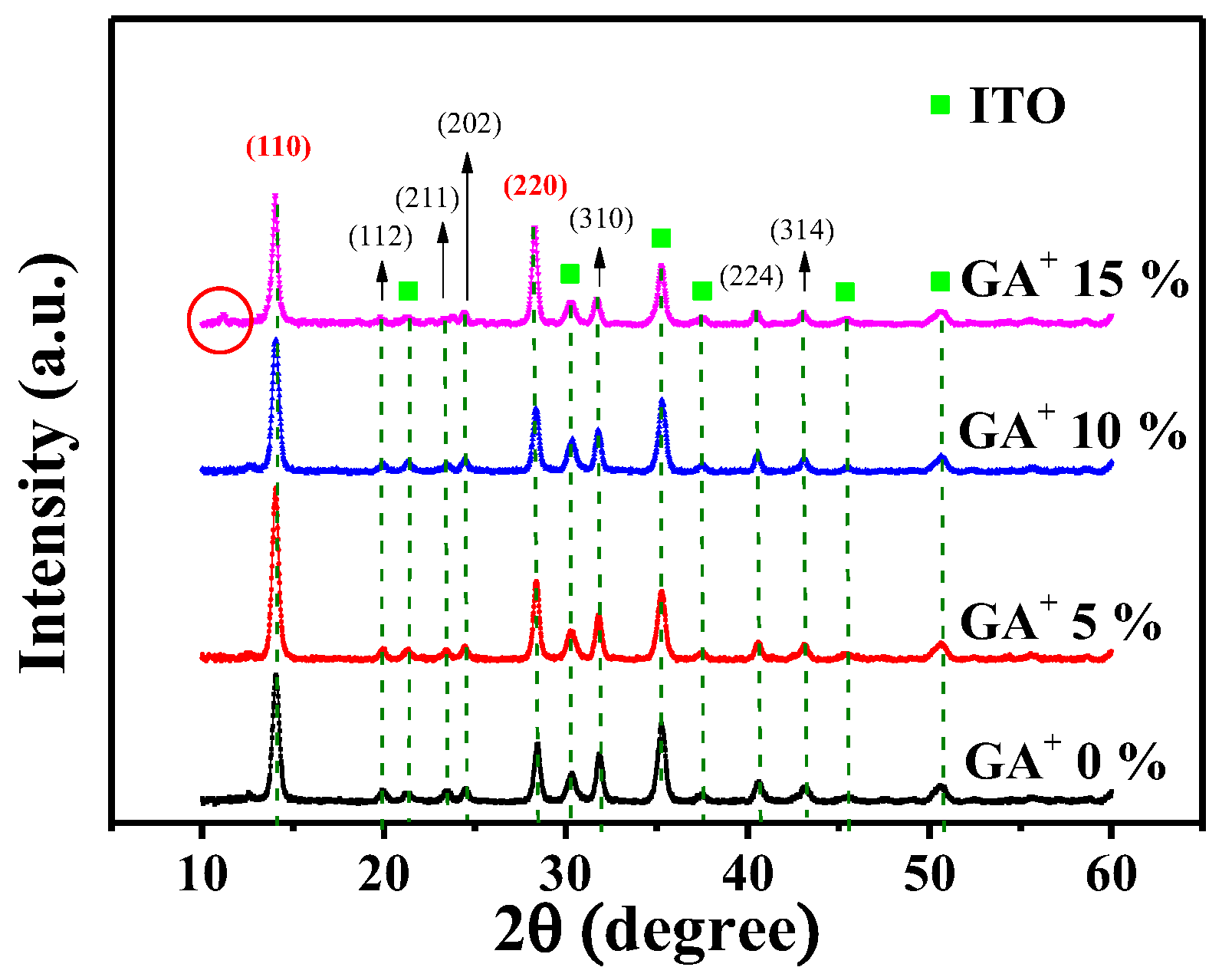
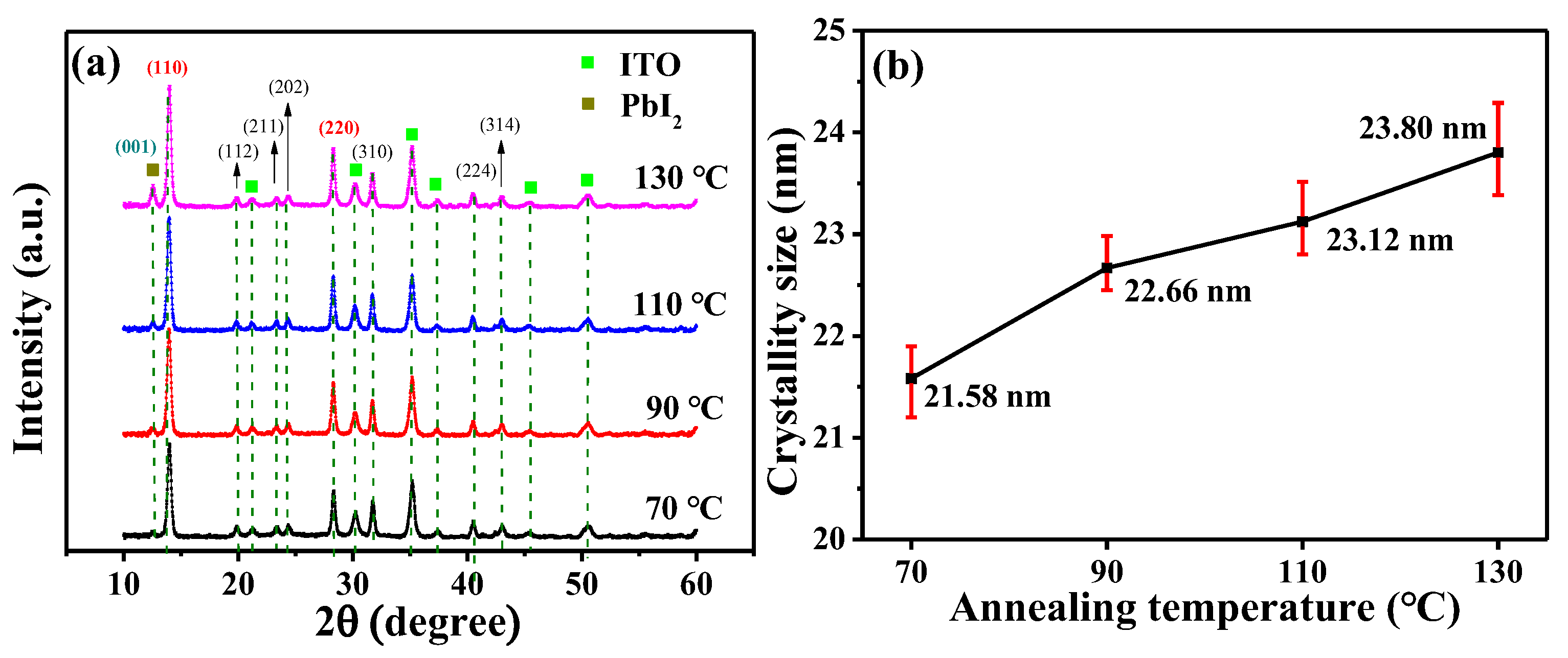
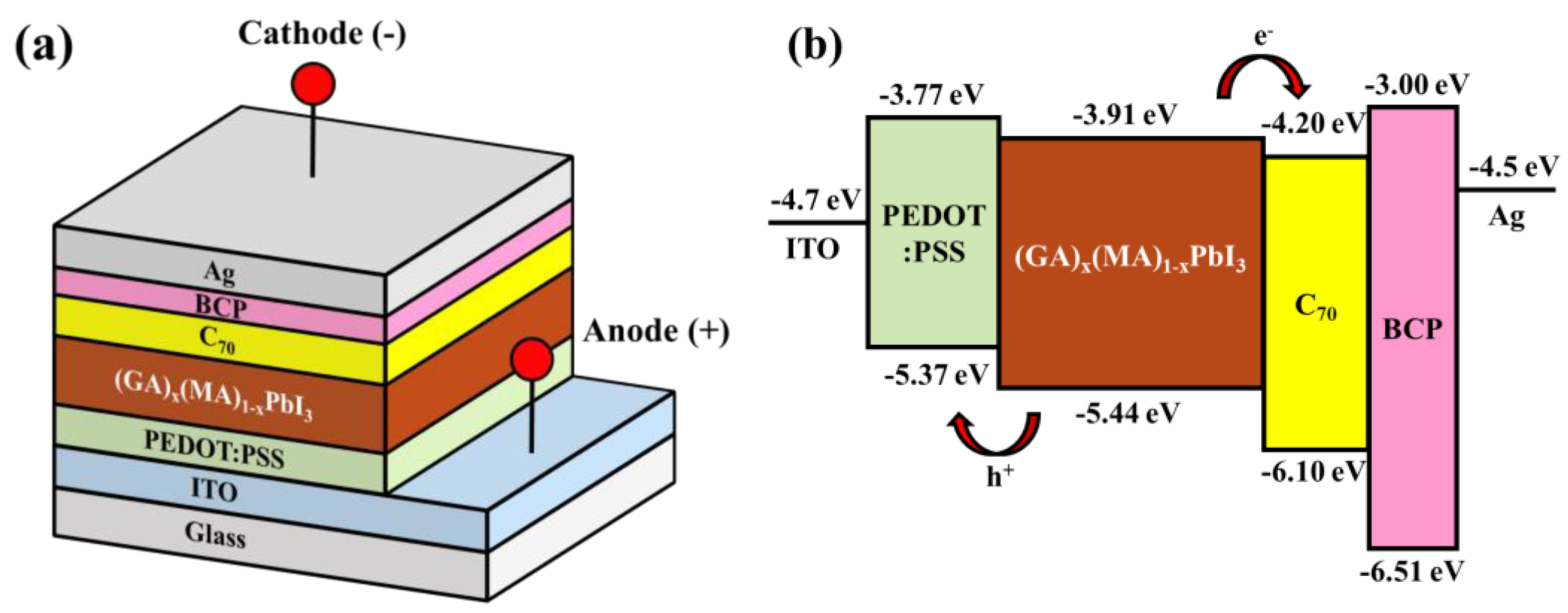
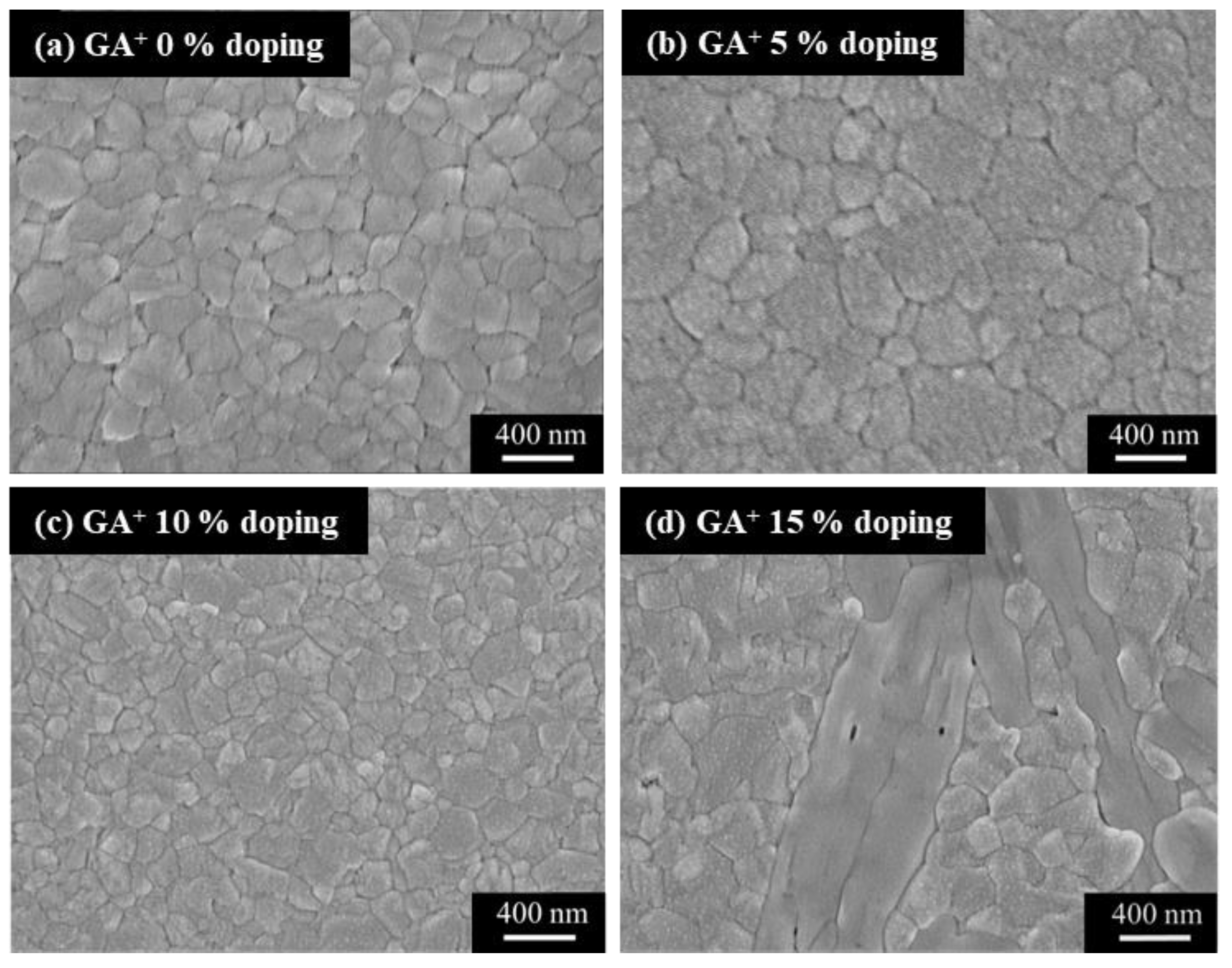
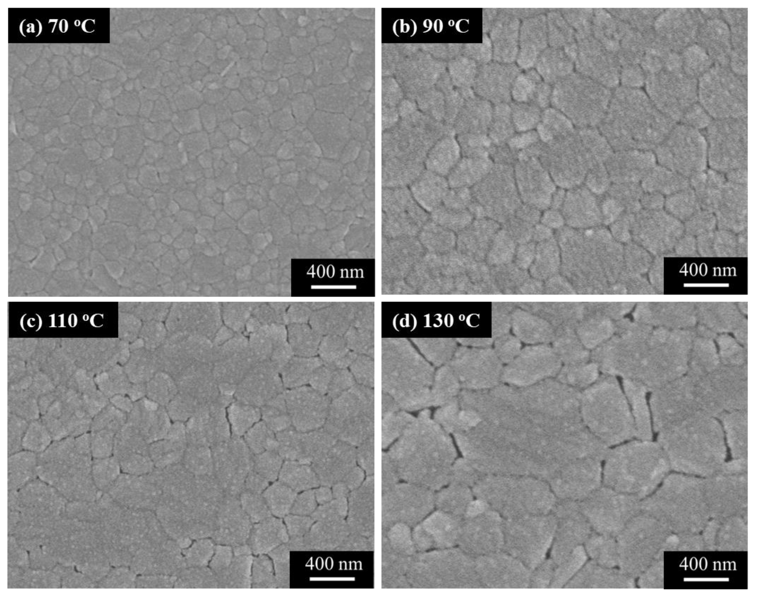
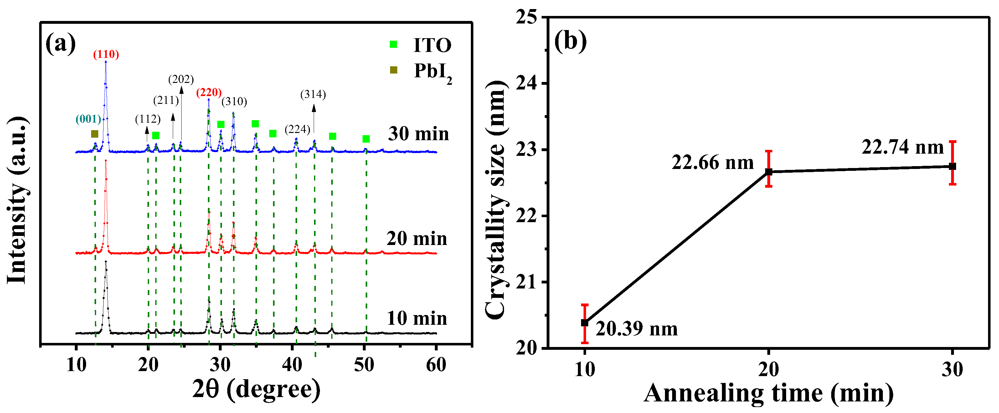
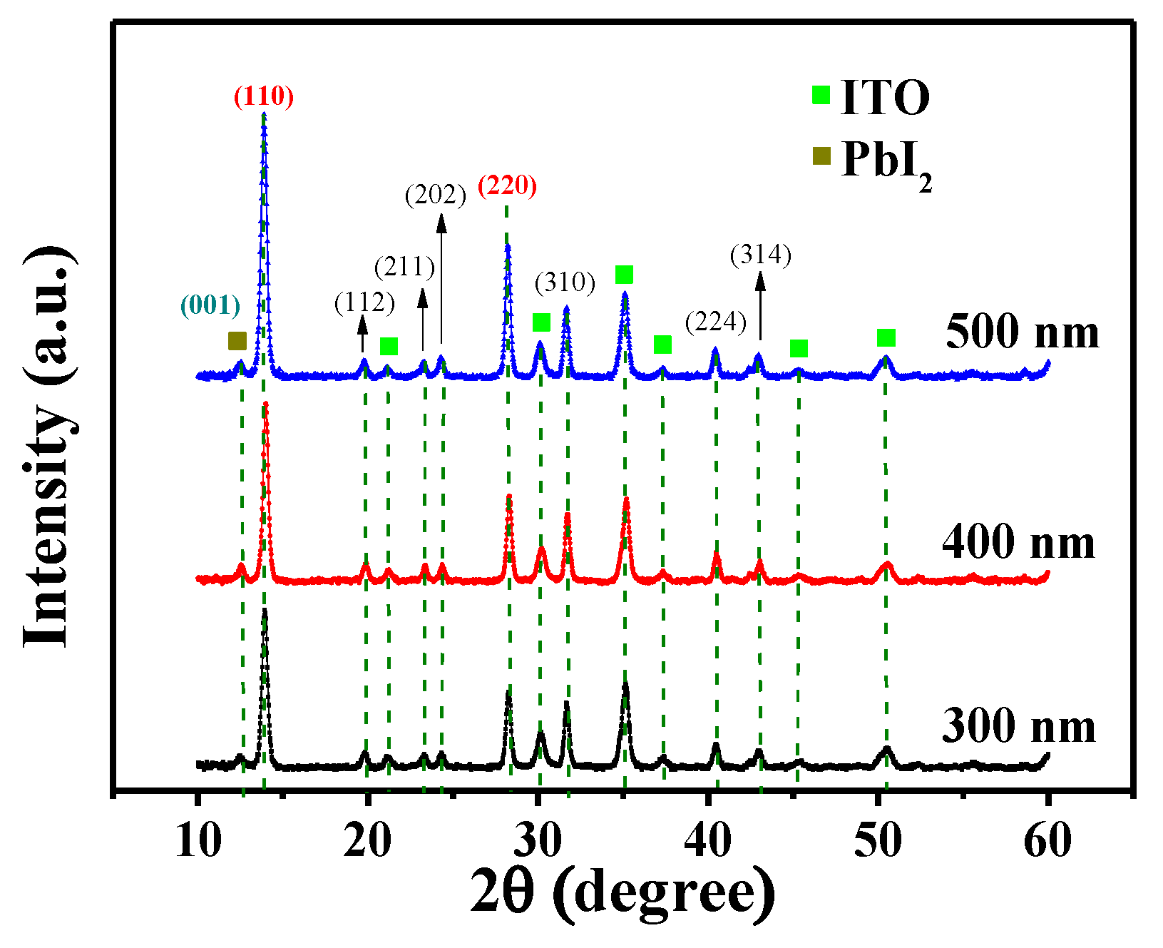
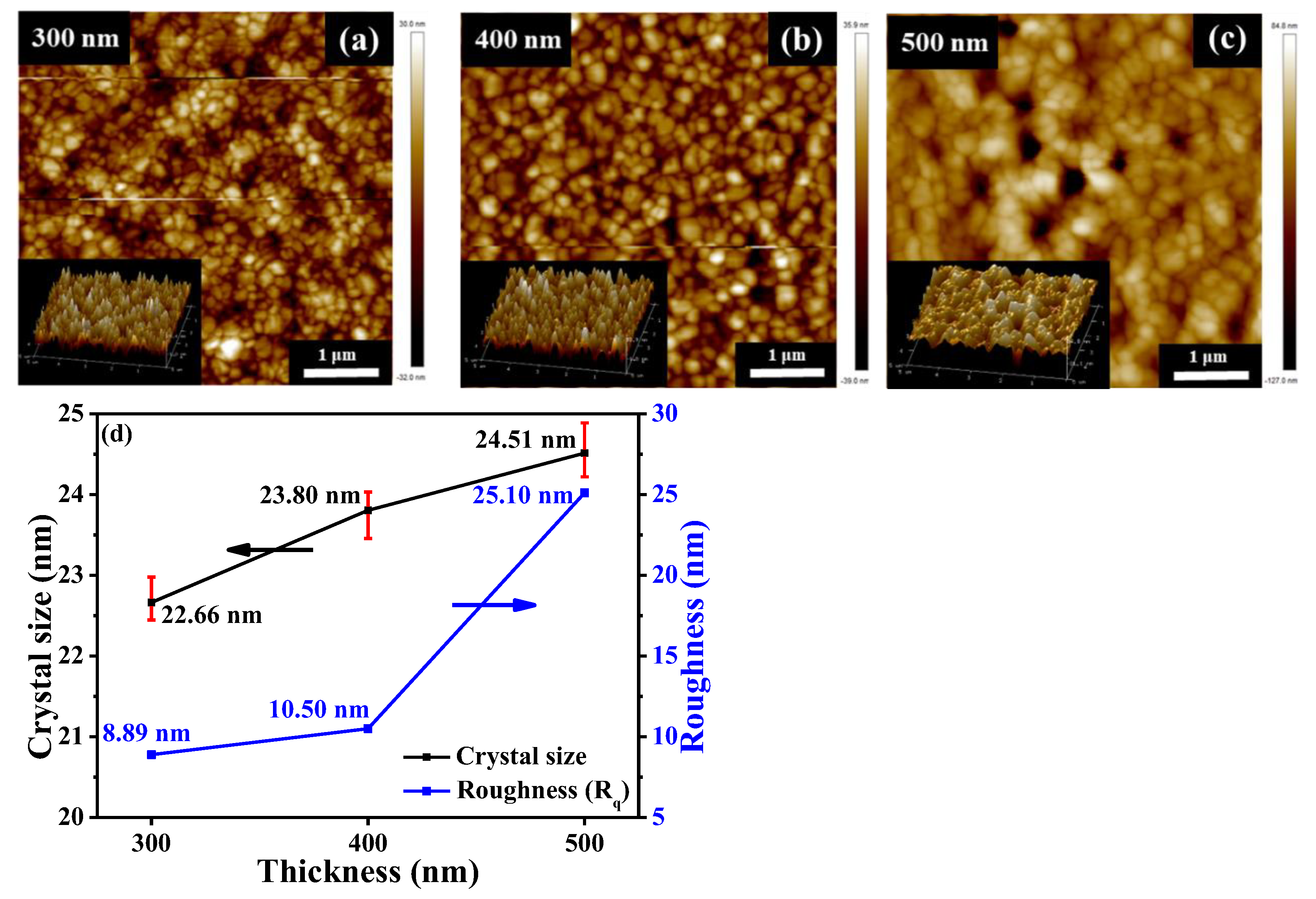
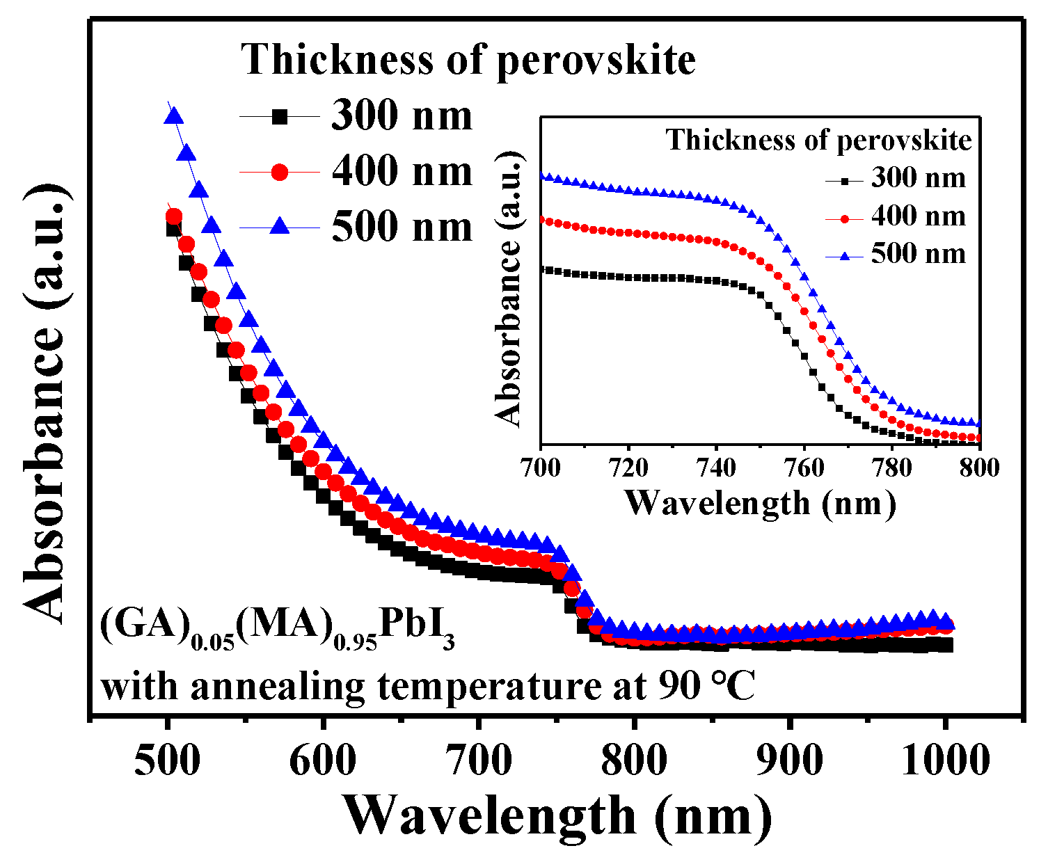
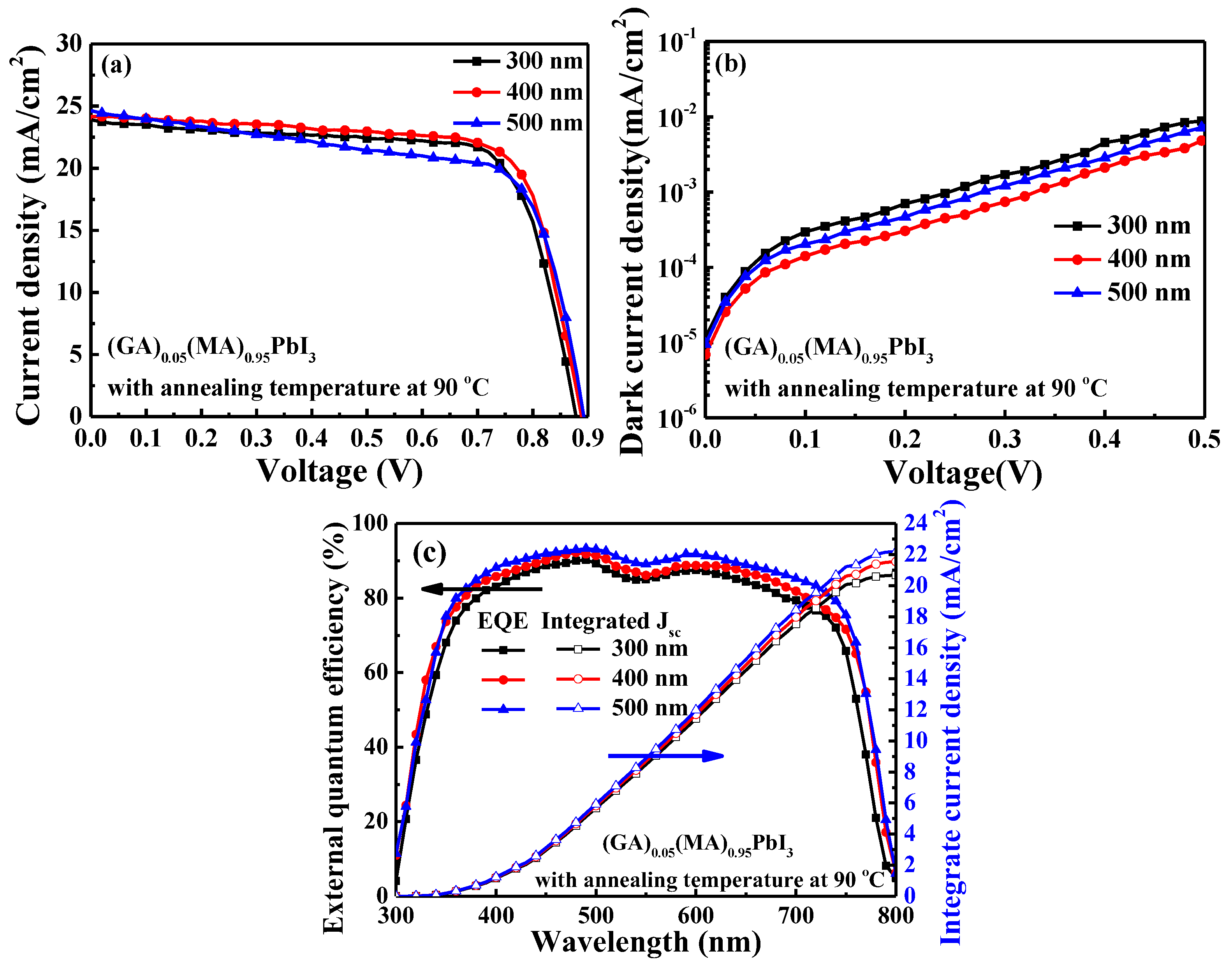
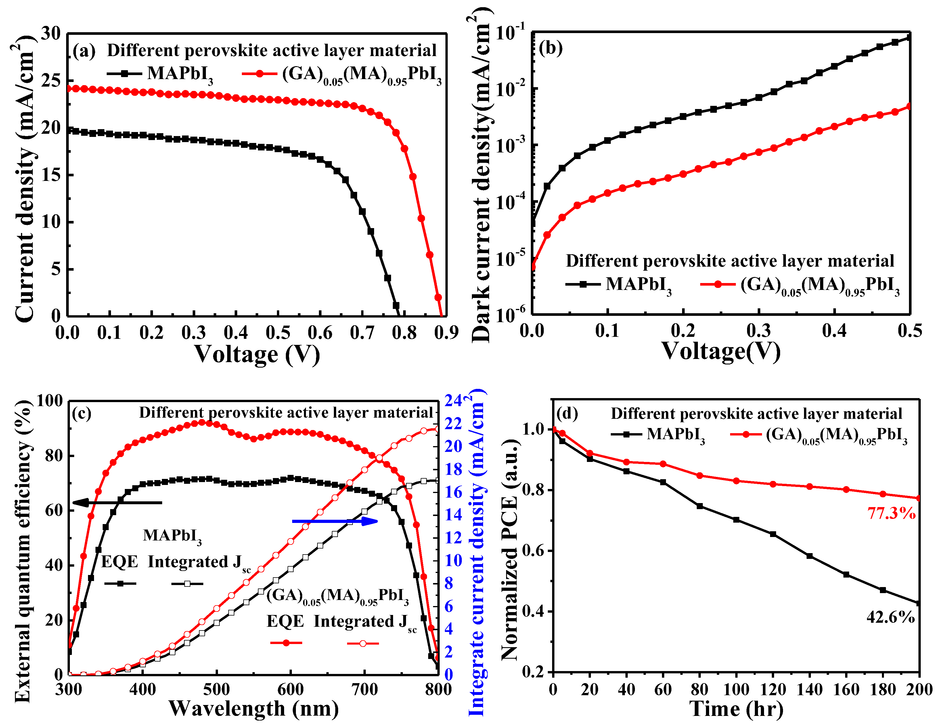
3. Experimental Results and Discussions

To achieve high-quality films, various GA+ doping concentrations of 0, 5, 10, and 15% were doped to obtain (GA)x(MA)1−xPbI3 films. The various 300-nm-thick (GA)x(MA)1−xPbI3 films were then annealed in a N2 ambient at 90 °C for 20 min. The XRD patterns, as shown in Figure 2, revealed the predominant (110) lattice plane of (GA)x(MA)1−xPbI3 films at 14.06°. As the GA+ doping concentration increased from 0% to 5%, a notable increase in the (110) peak intensity was observed at 5% GA+ doping concentration. This phenomenon was attributed to the fact that the GA+ had a better hydrogen bonding capability to construct a stronger perovskite crystal, which could enhance the crystallinity of the (GA)x(MA)1−xPbI3 films and increased the intensity of the (110) diffraction peak [30]. However, the intensity of the (110) diffraction peak attenuated as the doping concentration further increased to 10%. This attenuation was attributed to the fact that excess low-dimensional (GA)x(MA)1−xPbI3 perovskite crystals, generated by doping excess GA+, deteriorated the crystallinity of the original three-dimensional (GA)x(MA)1−xPbI3 film and reduced the carrier vertical transmission ability [31,32,33]. As the GA+ doping concentration further increased to 15%, it led to the generation of a new diffraction peak at 11.3°, indicating low-dimensional crystal growth during excess GA+-doped. Consequently, when the GA+ doping concentration was 5%, the (GA)x(MA)1−xPbI3 film exhibited the best crystallinity.
The SEM images shown in Figure 3 were used to investigate the surface morphology of the various (GA)x(MA)1−xPbI3 films. According to the SEM images, compared with the one without GA+ doping, the (GA)x(MA)1−xPbI3 films with a GA+ doping concentration of 5% displayed a larger crystal grain size. The phenomenon was attributed to the superior hydrogen bonding of GA+, which was evident from Figure 3a,b. Conversely, as shown in Figure 3c, aligning with XRD results, because the excess GA+ doping concentration deteriorated the crystallinity of the original three-dimensional perovskite, the crystal grain size of the (GA)x(MA)1−xPbI3 films was significantly decreased as the GA+ doping concentration increased to 10%. Moreover, according to Figure 3d, when the GA+ doping concentration further increased to 15%, a significant low-dimensional (GA)x(MA)1−xPbI3 perovskite crystal appeared on the surface. It also verified the GA+ indeed generated the low-dimensional (GA)x(MA)1−xPbI3 perovskite crystal, which corresponded to the diffraction peak at 11.3° shown in Figure 2. Consequently, the (GA)x(MA)1−xPbI3 films with GA+ doping concentration of 5% had the best surface morphology and crystallinity, which promoted the carrier transportation ability and enhanced performances of the resulting PSCs devices. The results from SEM images corresponded to the trend of XRD analysis. As a result, the (GA)x(MA)1−xPbI3 films with an optimal GA+ doping concentration of 5% was defined as (GA)0.05(MA)0.95PbI3.
The influence of various annealing temperatures of 70, 90, 110, and 130 °C on (GA)0.05(MA)0.95PbI3 films was also explored in this work. Figure 4a shows the XRD results of the 300-nm-thick (GA)0.05(MA)0.95PbI3 films annealed at various temperatures. Using the full width at half maximum (FWHM) of the (110) diffraction peak shown in Figure 4a, the crystal grain size (D) of the various (GA)0.05(MA)0.95PbI3 films could be calculated and shown in Figure 4b by the following Equation (1) [34]:
D = K λ β cos θ
where K represents the Scherrer constant, λ represents the wavelength of the X-ray, β represents the FWHM value of the main diffraction peak, and θ represents the diffraction angle. Each XRD and related crystal grain size analysis of the (GA)0.05(MA)0.95PbI3 films with various annealing temperatures had been measured over five times. The error bar presented in Figure 4b showed the statistical results of the XRD measurement. From the XRD results and the related crystal grain size presented in Figure 4a,b, when the annealing temperature increased from 70 °C to 130 °C, the crystallinity of the (GA)0.05(MA)0.95PbI3 films was enhanced and the associated crystal grain size was gently increased from 21.58 nm to 23.80 nm. This phenomenon was attributed to the fact that higher annealing temperature accelerated the formation kinetics of perovskite crystal, which could produce a perovskite film with better crystallinity and larger crystal grain size [35,36]. The larger crystal grain size was beneficial for the carrier transportation in the (GA)0.05(MA)0.95PbI3 films. However, along with the increasing annealing temperature, there was a diffraction peak gradually appearing at the angle of 12.56°, representing the (001) crystal plane of PbI2 molecules which originated from the degraded (GA)0.05(MA)0.95PbI3 perovskite crystal. The increasing annealing temperature also elevated the (001) diffraction peak intensity of PbI2 molecules. This phenomenon was attributed to the fact that the higher annealing temperature accelerated the degradation of (GA)0.05(MA)0.95PbI3, which tended to decompose into PbI2, MAI, and GAI molecules. It could easily generate pinholes and cracks on the perovskite surface. Consequently, the carrier transportation ability of the perovskite films deteriorated [37]. SEM surface analysis was used to further observe the surface morphology of the (GA)0.05(MA)0.95PbI3 films treated with various annealing temperatures. From the SEM images shown in Figure 5a–d, as the annealing temperature increased from 70 °C to 130 °C, the crystal grain size of the (GA)0.05(MA)0.95PbI3 films was indeed significantly increased due to the generation of higher formation kinetics, which could correspond to the results of XRD analysis in Figure 4. However, the higher annealing temperature also led to a higher decomposition rate. Consequently, pinholes and cracks were caused on the (GA)0.05(MA)0.95PbI3 films. As shown in Figure 5c, when the annealing temperature was 110 °C, pinholes and cracks appeared among the crystal boundaries of the annealed perovskite films. Compared to the (GA)0.05(MA)0.95PbI3 film annealed at a temperature of 110 °C, in addition to their larger crystal grain size, it also caused more pinholes and cracks residing on the perovskite films annealed at 130 °C, as shown in Figure 5d. Combining the results of XRD analysis and SEM images, when the annealing temperature of the (GA)0.05(MA)0.95PbI3 films was higher than 110 °C, many pinholes and cracks started to appear on the perovskite surface. It would seriously deteriorate the carrier transportation ability of the (GA)0.05(MA)0.95PbI3 perovskite films. To manufacture high-performance PSCs with an optimal (GA)0.05(MA)0.95PbI3 film, the best compromise among a larger perovskite crystal grain size, a lower decomposition rate, and less pinholes and cracks was needed to be investigated. Thus, to balance the crystal grain size, decomposition rate, and surface integrity, the temperature of 90 °C was identified as the optimal annealing temperature for fabricating high-performance PSCs in this work.
Figure 6a,b show the XRD patterns and the relating crystal grain size of the 300-nm-thick (GA)0.05(MA)0.95PbI3 films annealed for various times of 10, 20, and 30 min. The XRD patterns, as shown in Figure 6a, revealed the predominant (110) lattice plane of (GA)0.05(MA)0.95PbI3 films at 14.06°. According to the results, as the annealing time increased from 10 min to 20 min, the crystallinity of the (GA)0.05(MA)0.95PbI3 films was enhanced and the relating crystal grain size increased from 20.39 nm to 22.66 nm. This phenomenon illustrated under the annealing temperature of 90 °C, the annealing time of 10 min was not enough for obtaining the (GA)0.05(MA)0.95PbI3 films with high crystallinity. However, as the annealing time further increased from 20 min to 30 min, the diffraction peak of PbI2 molecules at 12.56° enhanced. This phenomenon was attributed to the fact that the excessive annealing time would also stimulate the degradation of (GA)0.05(MA)0.95PbI3 perovskite crystal and deteriorate the quality of (GA)0.05(MA)0.95PbI3 films. Besides, it did not present a significant enhancement of the relating crystal grain size of (GA)0.05(MA)0.95PbI3 films when the annealing time increased from 20 min to 30 min. The phenomenon showed if the annealing time exceeded 20 min, it would only stimulate the decomposition of (GA)0.05(MA)0.95PbI3 perovskite crystal but not generate the bigger (GA)0.05(MA)0.95PbI3 perovskite crystal grain size.
To study the impact of thickness variations in (GA)0.05(MA)0.95PbI3 films, ranging from 300 to 500 nm, the measured XRD results were shown in Figure 7. These various (GA)0.05(MA)0.95PbI3 films were annealed in a N2 ambient at 90 °C for 20 min. The crystallinity of various (GA)0.05(MA)0.95PbI3 films was found to be gradually elevated as the thickness increased from 300 nm to 500 nm. Based on the results in the stronger intensity of the (110) diffraction peak and the better crystallinity of the thicker (GA)0.05(MA)0.95PbI3 film, this above-mentioned phenomenon was attributed to the formation of denser perovskite molecules and multi-layered particle structures [38]. Because the better crystallinity and larger crystal grain size of the perovskite film led to increase carrier mobility within the polycrystalline structure, the performances of the resulting PSC devices were expected to be consequently enhanced. [39]. However, according to the results of AFM analysis presented in Figure 8a–c, the root-mean-square roughness (Rq) of the (GA)0.05(MA)0.95PbI3 films increased from 8.50 nm to 10.50 nm and to 25.10 nm as the thickness of the films increased from 300 nm to 400 nm and to 500 nm. If the surface of the perovskite films was seriously roughened, more defects would be easily generated within the interface during the coverage of the following transport layer. The undesired defects could seriously deteriorate the carrier transportation ability of the resulting PSCs [40,41]. Consequently, the large roughness would bring some adverse influences on the performances of the (GA)0.05(MA)0.95PbI3 films. Figure 8d shows the related crystal grain size, calculated from Figure 7 and Equation (1), and Rq as a function of the thickness of the (GA)0.05(MA)0.95PbI3 films. Each XRD pattern and related crystal grain size analysis of the (GA)0.05(MA)0.95PbI3 films with various thicknesses had been measured over five times. The error bar presented in Figure 8d showed the statistical results of the XRD measurement. As above-mentioned crystal grain size and Rq of the (GA)0.05(MA)0.95PbI3 films, despite larger crystal grain sizes of the (GA)0.05(MA)0.95PbI3 film with a thickness of 500 nm being beneficial for carrier mobility, the associated excessive roughness would adversely affect the performance of the resulting PSCs. Accordingly, to determine the optimal thickness of the (GA)0.05(MA)0.95PbI3 film, an optimal balance between a larger perovskite crystal grain size and a smaller roughness was needed to be investigated. The performances of the resulting PSCs with various thicknesses of the (GA)0.05(MA)0.95PbI3 films were analyzed to ascertain the optimal thickness of the (GA)0.05(MA)0.95PbI3 perovskite active layer.
Figure 9 shows the absorption spectra of the various-thick (GA)0.05(MA)0.95PbI3 perovskite films. It was found the thicker perovskite films exhibited enhanced light absorption. The inserted figure in Figure 9 extended the absorption spectra from the wavelength of 700 nm to 800 nm. It demonstrated a significant change in light absorbance of the perovskite active layer with different thicknesses. When the thickness of the (GA)0.05(MA)0.95PbI3 perovskite film was 500 nm, it exhibited the highest light absorbance. The higher light absorbance of the perovskite active layer could absorb more photons to generate more carriers and enhance the short-circuit current density (Jsc) of the resulting PSCs. Furthermore, because the better crystallinity caused in a thicker film could improve the carrier transport properties, the (GA)0.05(MA)0.95PbI3 perovskite active layer with increasing thickness could be expected to also enhance the Jsc of the resulting PSCs [42,43]. The current density-voltage, dark current density-voltage and external quantum efficiency (EQE) performances of the PSCs using the (GA)0.05(MA)0.95PbI3 perovskite active layer with a thickness of 300, 400, and 500 nm were illustrated in Figure 10a–c, respectively. The experimental results were also listed in Table 1. As shown in Figure 10a, in view of the higher light absorbance, better crystallinity, and larger crystal grain size, when the thickness of the (GA)0.05(MA)0.95PbI3 perovskite active layer increased from 300 nm to 400 nm, the Jsc of the resulting PSCs gradually increased from 23.88 mA/cm2 to 24.21 mA/cm2, which increased the PCE from 15.36% to 15.78%. However, although the Jsc of the PSCs could increase from 24.21 mA/cm2 to 24.75 mA/cm2 as the thickness of the (GA)0.05(MA)0.95PbI3 perovskite active layer further increased from 400 nm to 500 nm, the fill factor (FF) of the PSCs was relatively decreased from 73.1% to 66.6%. The deterioration in FF was attributed to the factor that the markedly increasing roughness of the 500-nm-thick (GA)0.05(MA)0.95PbI3 perovskite layer generated more defects at the interface of the (GA)0.05(MA)0.95PbI3 perovskite active layer and the subsequent fullerene C70 ETL. Consequently, the PCE of the resulting PSCs decreased from 15.78% to 14.73% as the thickness of the (GA)0.05(MA)0.95PbI3 perovskite active layer increased from 400 nm to 500 nm. Furthermore, the dark current density-voltage characteristics of PSCs using the various-thick (GA)0.05(MA)0.95PbI3 perovskite active layers were shown in Figure 10b. When the thickness of (GA)0.05(MA)0.95PbI3 perovskite active layer was 400 nm, it exhibited the lowest dark current. This was attributed to the phenomenon the better crystallinity could improve the carrier transport properties and the lower roughness could reduce the number of defects residing at the interface of the (GA)0.05(MA)0.95PbI3 perovskite active layer and the fullerene C70 ETL. On the basis of the illustration above, the optimal balance between the crystal grain size and the roughness occurred at the 400-nm-thick (GA)0.05(MA)0.95PbI3 perovskite active layer. The best performance of the resulting PSCs with an open-circuit voltage (Voc) of 0.891 V, Jsc of 24.21 mA/cm2, FF of 73.1%, and PCE of 15.78% were obtained. Since EQE is an important parameter for characterizing PSCs to assess their quality, Figure 10c shows the dependence of EQE on wavelength (300–800 nm) of the various PSCs. Besides, the integrated Jsc is also used to verify the value and trend of Jsc of the PSCs. Using the EQE spectra, integrated Jsc can be calculated by the following Equation (2) [44]:
Integrated   J sc = EQE λ × qF λ AM 1.5 G d λ
where F(λ) represents the wavelength (λ)-dependent incident photon flux density of AM 1.5G standard spectroscopy, EQE(λ) represents the wavelength-dependent external quantum efficiency, and q represents the electron charge. The integrated Jsc of the PSCs using the (GA)0.05(MA)0.95PbI3 perovskite active layer with the thicknesses of 300, 400, and 500 nm was 20.69, 21.55, and 22.21 mA/cm2, respectively. According to the results, although the PSCs using the 500-nm-thick (GA)0.05(MA)0.95PbI3 perovskite active layer revealed the highest EQE due to the higher light absorptance and the better crystallinity, the markedly increasing roughness would still deteriorate the FF and PCE performances of PSCs from 73.1% to 66.6% and from 15.78% to 14.73%, respectively. Synthesizing the aforementioned results, to achieve the best PCE performance, the optimal 400-nm-thick (GA)0.05(MA)0.95PbI3 perovskite active layer of PSCs was determined.
Figure 11a–c show the current density-voltage, dark current density-voltage and EQE performances of the PSCs with MAPbI3 perovskite active layer and with optimal (GA)0.05(MA)0.95PbI3 perovskite active layer, respectively. The relating experimental results were listed in Table 2. Compared with the one without GA+ doping, the PSCs with optimal (GA)0.05(MA)0.95PbI3 perovskite active layer showed a significant enhancement of device performance, which led to the Voc being promoted from 0.783 V to 0.891 V, the Jsc increased from 19.71 mA/cm2 to 24.21 mA/cm2, the FF elevated from 65.0% to 73.1, and the PCE enhanced from 10.03% to 15.78%, respectively. The phenomenon was attributed to the fact that the better hydrogen bonding capability of GA+ could construct a stronger perovskite crystal and enhance the crystallinity of the perovskite active layer. Furthermore, after the optimization of doping concentration, annealing temperature and time, and thickness of (GA)0.05(MA)0.95PbI3 perovskite active layer, not only the device performance but also the stability of PSCs could be enhanced. Figure 11d illustrates the 200-h stability test of the PSCs with MAPbI3 perovskite active layer and with optimal (GA)0.05(MA)0.95PbI3 perovskite active layer, respectively. According to the results, after a 200-h stability test at the atmospheric environment with an ambient temperature of 25 °C and the relative humidity of 50%, the PSCs without GA+ only retained 42.6% of its original PCE, while 77.3% of the original PCE was retained by the PSCs with the optimal (GA)0.05(MA)0.95PbI3 perovskite active layer. This enhanced stability was attributed to GA+’s superior hydrogen bonding capability, which strengthens the crystal structure of the (GA)0.05(MA)0.95PbI3 perovskite active layer. Consequently, GA+ doping not only improved performance but also significantly boosted the long-term stability of the resulting PSCs.

4. Conclusions

In summary, based on the XRD and SEM analyses, owing to the GA+’s superior hydrogen bonding capability in constructing stronger perovskite crystals, the perovskite active film with a GA+ doping concentration of 5% was demonstrated as optimal film for superior crystallinity and surface morphology. The XRD and SEM results also demonstrated a higher annealing temperature was beneficial for better crystallinity and larger crystal grain size. However, this higher annealing temperature also increased the decomposition rate of the (GA)0.05(MA)0.95PbI3 films, simultaneously. By effectively balancing enhanced crystal growth against decomposition risks, the optimal annealing temperature and time was determined to be 90 °C and 20 min, respectively. Combining the results of XRD and AFM measurements, it was found the better crystallinity and the roughened texture of the (GA)0.05(MA)0.95PbI3 perovskite active layer were obtained as its thickness increased. When the thickness of the (GA)0.05(MA)0.95PbI3 films increased from 400 nm to 500 nm, the significantly induced defects caused by the serious roughness could deteriorate the performances of the resulting PSCs. Consequently, the 400-nm-thick ((GA)0.05(MA)0.95PbI3 perovskite active layer emerged as an optimal thickness. From the performance analysis of PSCs, when the thickness of the (GA)0.05(MA)0.95PbI3 perovskite active layer was 400 nm, it had optimal performance, with PCE, Jsc, Voc, and FF of 15.78%, 24.21 mA/cm2, 0.891 V, and 73.1%, respectively. Notably, PSCs with the optimal (GA)0.05(MA)0.95PbI3 layer demonstrated significantly improved device performances, whose PCE increased from 10.03% to 15.78%. According to the experimental results, by doping GA+ into MAPbI3 perovskite films, not only performances improved but also long-term stability of the resulting (GA)0.05(MA)0.95PbI3 films, retaining 77.3% of their original PCE after stability test for 200 h compared with the 42.6% without GA+ additive doping. Consequently, using the optimal (GA)0.05(MA)0.95PbI3 perovskite active layers, the resulting PSCs with high performances and high stability have been successfully obtained.

Author Contributions

Conceptualization, C.-T.L. and H.-Y.L.; data curation, T.-C.C. and H.-Y.L.; funding acquisition, C.-T.L. and H.-Y.L.; investigation, T.-C.C. and H.-Y.L.; writing—original draft, T.-C.C.; writing—review and editing, C.-T.L. and H.-Y.L. All authors have read and agreed to the published version of the manuscript.

Funding

This work was supported by the National Science and Technology Council (NSTC), Republic of China under Contract No. NSTC 112-2221-E-006-121-MY2, NSTC 112-2923-E-006-006, and MOST-111-2221-E-006-229-MY3.

Data Availability Statement

The data presented in this study are available upon request from the corresponding author.

Acknowledgments

The authors are grateful for the facilities and other support given by the National Science and Technology Council (NSTC), Republic of China under Contract No. NSTC 112-2221-E-006-121-MY2, NSTC 112-2923-E-006-006, and MOST-111-2221-E-006-229-MY3. The authors also gratefully acknowledge the use of EM000600 and XRD005101 equipment provided by the Core Facility Center of National Cheng Kung University.

Conflicts of Interest

The authors declare no conflict of interest.

References

  1. Diffenbaugh, N.S.; Burke, M. Global warming has increased global economic inequality. Proc. Natl. Acad. Sci. USA 2019, 116, 9808–9813. [Google Scholar] [CrossRef]
  2. Martinez-Anido, C.B.; Botor, B.; Florita, A.R.; Draxl, C.; Lu, S.; Hamann, H.F.; Hodge, B.M. The value of day-ahead solar power forecasting improvement. Sol. Energy 2016, 129, 192–203. [Google Scholar] [CrossRef]
  3. Wang, Z.F.; Li, X.; Yao, Z.H.; Zhang, M.M. Concentrating solar power development in China. J. Sol. Energy Eng. Trans.-ASME 2010, 132, 021203. [Google Scholar] [CrossRef]
  4. Yun, S.N.; Qin, Y.; Uhl, A.R.; Vlachopoulos, N.; Yin, M.; Li, D.D.; Han, X.G.; Hagfeldt, A. New-generation integrated devices based on dye-sensitized and perovskite solar cells. Energy Environ. Sci. 2018, 11, 476–526. [Google Scholar] [CrossRef]
  5. Lin, H.; Wang, W.L.; Liu, Y.Z.; Li, X.; Li, J.B. New trends for solar cell development and recent progress of dye sensitized solar cells. Front. Mater. Sci. 2009, 3, 345–352. [Google Scholar] [CrossRef]
  6. Assadi, M.K.; Bakhoda, S.; Saidur, R.; Hanaei, H. Recent progress in perovskite solar cells. Renew. Sust. Energ. Rev. 2018, 81, 2812–2822. [Google Scholar] [CrossRef]
  7. Xiong, S.B.; Hao, T.Y.; Sun, Y.Y.; Yang, J.M.; Ma, R.R.; Wang, J.L.; Gong, S.J.; Liu, X.J.; Ding, L.M.; Fahlman, M.; et al. Defect passivation by nontoxic biomaterial yields 21% efficiency perovskite solar cells. J. Energy Chem. 2021, 55, 265–271. [Google Scholar] [CrossRef]
  8. Valadi, K.; Gharibi, S.; Taheri-Ledari, R.; Akin, S.; Maleki, A.; Shalan, A.E. Metal oxide electron transport materials for perovskite solar cells: A review. Environ. Chem. Lett. 2021, 19, 2185–2207. [Google Scholar] [CrossRef]
  9. Jiang, Q.; Zhang, X.W.; You, J.B. SnO2: A wonderful electron transport layer for perovskite solar cells. Small 2018, 14, 1801154. [Google Scholar] [CrossRef]
  10. Yang, J.Y.; Luo, X.R.; Zhou, Y.K.; Li, Y.Y.; Qiu, Q.Q.; Xie, T.F. Recent advances in inverted perovskite solar cells: Designing and fabrication. Int. J. Mol. Sci. 2022, 23, 11792. [Google Scholar] [CrossRef]
  11. Zuo, C.T.; Bolink, H.J.; Han, H.W.; Huang, J.S.; Cahen, D.; Ding, L.M. Advances in perovskite solar cells. Adv. Sci. 2016, 3, 1500324. [Google Scholar] [CrossRef]
  12. Park, N.G.; Segawa, H. Research direction toward theoretical efficiency in perovskite solar cells. ACS Photonics 2018, 5, 2970–2977. [Google Scholar] [CrossRef]
  13. Yang, H.Y.; Chuquer, A.; Han, S.H.; Gaudel, G.S.; Pham, X.H.; Kim, H.M.; Yun, W.J.; Jun, B.H.; Rho, W.Y. Optimizing the aspect ratio of nanopatterned mesoporous TiO2 thin-film layer to improve energy conversion efficiency of perovskite solar cells. Int. J. Mol. Sci. 2021, 22, 12235. [Google Scholar] [CrossRef] [PubMed]
  14. Green, M.A.; Dunlop, E.D.; Yoshita, M.; Kopidakis, N.; Bothe, K.; Siefer, G.; Hao, X.J. Solar cell efficiency tables (version 62). Prog. Photovolt. 2023, 31, 651–663. [Google Scholar] [CrossRef]
  15. Chang, T.C.; Liao, C.Y.; Lee, C.T.; Lee, H.Y. Investigation of the performance of perovskite solar cells with ZnO-covered PC61BM electron transport layer. Materials 2023, 16, 5061. [Google Scholar] [CrossRef] [PubMed]
  16. Chen, G.S.; Chen, Y.C.; Lee, C.T.; Lee, H.Y. Performance improvement of perovskite solar cells using electron and hole transport layers. Sol. Energy 2018, 174, 897–900. [Google Scholar] [CrossRef]
  17. Wang, D.; Wright, M.; Elumalai, N.K.; Uddin, A. Stability of perovskite solar cells. Sol. Energy Mater. Sol. Cells 2016, 147, 255–275. [Google Scholar] [CrossRef]
  18. Alkahtani, M.; Alenzi, S.M.; Alsolami, A.; Alsofyani, N.; Alfahd, A.; Alzahrani, Y.A.; Aljuwayr, A.; Abduljawad, M. High-performance and stable perovskite solar cells using carbon quantum dots and upconversion nanoparticles. Int. J. Mol. Sci. 2022, 23, 14441. [Google Scholar] [CrossRef] [PubMed]
  19. Jabeen, N.; Zaidi, A.; Hussain, A.; Ul Hassan, N.; Ali, J.; Ahmed, F.; Khan, M.U.; Iqbal, N.; Elnasr, T.A.S.; Helal, M.H. Single- and multilayered perovskite thin films for photovoltaic applications. Nanomaterials 2022, 12, 3208. [Google Scholar] [CrossRef]
  20. Chang, K.C.; Yeh, T.H.; Lee, H.Y.; Lee, C.T. High performance perovskite solar cells using multiple hole transport layer and modulated FAxMA1−xPbI3 active layer. J. Mater. Sci. Mater. Electron. 2020, 31, 4135–4141. [Google Scholar] [CrossRef]
  21. Wu, H.T.; Cheng, Y.T.; Leu, C.C.; Wu, S.H.; Shih, C.F. Improving two-step prepared CH3NH3PbI3 perovskite solar cells by Co-doping potassium halide and water in PbI2 layer. Nanomaterials 2019, 9, 666. [Google Scholar] [CrossRef] [PubMed]
  22. Wang, S.; Xu, Y.K.; Wang, Q.; Zhou, X.F.; Li, Z.H.; Wang, M.; Lei, Y.T.; Zhang, H.; Wang, H.X.; Jin, Z.W. Guanidium-assisted crystallization engineering for highly efficient CsPbI3 solar cells. J. Mater. Chem. C 2022, 10, 8234–8240. [Google Scholar] [CrossRef]
  23. Zheng, Y.F.; Yang, X.Y.; Su, R.; Wu, P.; Gong, Q.H.; Zhu, R. High-performance CsPbIxBr3-x all-inorganic perovskite solar cells with efficiency over 18% via spontaneous interfacial manipulation. Adv. Funct. Mater. 2020, 30, 2000457. [Google Scholar] [CrossRef]
  24. Nam, J.E.; Jo, H.J.; Kang, J.K.; Woo, S.; Hwang, D.K. Optimization of electrolyte components on the performance of organic-dye-sensitized solar cells. J. Nanosci. Nanotechnol. 2017, 17, 8100–8104. [Google Scholar] [CrossRef]
  25. Jeanbourquin, X.A.; Li, X.E.; Law, C.; Barnes, P.R.F.; Humphry-Baker, R.; Lund, P.; Asghar, M.I.; O’Regan, B.C. Rediscovering a key interface in dye-sensitized solar cells: Guanidinium and iodine competition for binding sites at the dye/electrolyte surface. J. Am. Chem. Soc. 2014, 136, 7286–7294. [Google Scholar] [CrossRef] [PubMed]
  26. Kishimoto, T.; Oku, T.; Suzuki, A.; Ueoka, N. Additive effects of guanidinium iodide on CH3NH3PbI3 perovskite solar cells. Phys. Status Solidi A Appl. Mat. 2021, 218, 2100396. [Google Scholar] [CrossRef]
  27. Pan, W.C.; Lin, J.M.; Wu, J.H.; Rong, B.; Zhang, X.P.; Chen, Q.; Zhang, M.; Wang, S.B.; Sun, W.H.; Wang, X.B.; et al. Interface modification by formamidine acetate for efficient perovskite solar cells. Sol. Energy 2022, 232, 304–311. [Google Scholar] [CrossRef]
  28. Jodlowski, A.D.; Roldán-Carmona, C.; Grancini, G.; Salado, M.; Ralaiarisoa, M.; Ahmad, S.; Koch, N.; Camacho, L.; De Miguel, G.; Nazeeruddin, M.K. Large guanidinium cation mixed with methylammonium in lead iodide perovskites for 19% efficient solar cells. Nat. Energy 2017, 2, 972–979. [Google Scholar] [CrossRef]
  29. Liu, C.; Liu, S.; Wang, Y.F.; Chu, Y.M.; Yang, K.; Wang, X.D.; Gao, C.X.; Wang, Q.F.; Du, J.K.; Li, S.; et al. Improving the performance of perovskite solar cells via a novel additive of N,1-fluoroformamidinium iodide with electron-withdrawing fluorine group. Adv. Funct. Mater. 2021, 31, 2010603. [Google Scholar] [CrossRef]
  30. Li, W.; Thirumurugan, A.; Barton, P.T.; Lin, Z.S.; Henke, S.; Yeung, H.H.M.; Wharmby, M.T.; Bithell, E.G.; Howard, C.J.; Cheetham, A.K. Mechanical tunability via hydrogen bonding in metal–organic frameworks with the perovskite architecture. J. Am. Chem. Soc. 2014, 136, 7801–7804. [Google Scholar] [CrossRef]
  31. De Marco, N.; Zhou, H.P.; Chen, Q.; Sun, P.Y.; Liu, Z.H.; Meng, L.; Yao, E.P.; Liu, Y.S.; Schiffer, A.; Yang, Y. Guanidinium: A route to enhanced carrier lifetime and open-circuit voltage in hybrid perovskite solar cells. Nano Lett. 2016, 16, 1009–1016. [Google Scholar] [CrossRef]
  32. Hoang, M.T.; Pannu, A.S.; Yang, Y.; Madani, S.; Shaw, P.; Sonar, P.; Tesfamichael, T.; Wang, H.X. Surface treatment of inorganic CsPbI3 nanocrystals with guanidinium iodide for efficient perovskite light-emitting diodes with high brightness. Nano-Micro Lett. 2022, 14, 69. [Google Scholar] [CrossRef]
  33. Sarkar, K.; Mukherjee, S.; Mukherjee, S.; Mitra, M.K. Synthesis, characterization and studies on optical, dielectric and magnetic properties of undoped and cobalt doped nanocrystalline bismuth ferrite. J. Inst. Eng. India Ser. D 2014, 95, 135–143. [Google Scholar] [CrossRef]
  34. He, K.; Chen, N.F.; Wang, C.J.; Wei, L.S.; Chen, J.K. Method for determining crystal grain size by X-ray diffraction. Cryst. Res. Technol. 2018, 53, 1700157. [Google Scholar] [CrossRef]
  35. Choi, H.; Choi, K.; Choi, Y.; Kim, T.; Lim, S.; Park, T. A review on reducing grain boundaries and morphological improvement of perovskite solar cells from methodology and material-based perspectives. Small Methods 2020, 4, 1900569. [Google Scholar] [CrossRef]
  36. Zhang, L.; Hu, T.L.; Li, J.L.; Zhang, L.; Li, H.T.; Lu, Z.L.; Wang, G. All-inorganic perovskite solar cells with both high open-circuit voltage and stability. Front. Mater. 2020, 6, 330. [Google Scholar] [CrossRef]
  37. Kazemi, M.A.A.; Jamali, A.; Sauvage, F. A holistic study on the effect of annealing temperature and time on CH3NH3PbI3-based perovskite solar cell characteristics. Front. Energy Res. 2021, 9, 732886. [Google Scholar] [CrossRef]
  38. Xia, B.; Wu, Z.X.; Dong, H.; Xi, J.; Wu, W.; Lei, T.; Xi, K.; Yuan, F.; Jiao, B.; Xiao, L.X.; et al. Formation of ultrasmooth perovskite films toward highly efficient inverted planar heterojunction solar cells by micro-flowing anti-solvent deposition in air. J. Mater. Chem. A 2016, 4, 6295–6303. [Google Scholar] [CrossRef]
  39. Nukunudompanich, M.; Budiutama, G.; Suzuki, K.; Hasegawa, K.; Ihara, M. Dominant effect of the grain size of the MAPbI3 perovskite controlled by the surface roughness of TiO2 on the performance of perovskite solar cells. Crystengcomm 2020, 22, 2718–2727. [Google Scholar] [CrossRef]
  40. Liu, D.Y.; Gangishetty, M.K.; Kelly, T.L. Effect of CH3NH3PbI3 thickness on device efficiency in planar heterojunction perovskite solar cells. J. Mater. Chem. A 2014, 2, 19873–19881. [Google Scholar] [CrossRef]
  41. Momblona, C.; Malinkiewicz, O.; Roldan-Carmona, C.; Soriano, A.; Gil-Escrig, L.; Bandiello, E.; Scheepers, M.; Edri, E.; Bolink, H.J. Efficient methylammonium lead iodide perovskite solar cells with active layers from 300 to 900 nm. APL Mater. 2014, 2, 081504. [Google Scholar] [CrossRef]
  42. Xiao, M.D.; Huang, F.Z.; Huang, W.C.; Dkhissi, Y.; Zhu, Y.; Etheridge, J.; Gray-Weale, A.; Bach, U.; Cheng, Y.B.; Spiccia, L. A fast deposition-crystallization procedure for highly efficient lead iodide perovskite thin-film solar cells. Angew. Chem.-Int. Edit. 2014, 53, 9898–9903. [Google Scholar] [CrossRef] [PubMed]
  43. Rai, M.; Wong, L.H.; Etgar, L. Effect of perovskite thickness on electroluminescence and solar cell conversion efficiency. J. Phys. Chem. Lett. 2020, 11, 8189–8194. [Google Scholar] [CrossRef] [PubMed]
  44. Cerdán-Pasarán, A.; López-Luke, T.; Esparza, D.; Zarazúa, I.; De la Rosa, E.; Fuentes-Ramírez, R.; Alatorre-Ordaz, A.; Sánchez-Solís, A.; Torres-Castrod, A.; Zhang, J.Z. Photovoltaic properties of multilayered quantum dot/quantum rod-sensitized TiO2 solar cells fabricated by SILAR and electrophoresis. Phys. Chem. Chem. Phys. 2015, 17, 18590–18599. [Google Scholar] [CrossRef] [PubMed]
Figure 1. (a) Schematic configuration and (b) corresponding energy level diagram of perovskite solar cells with (GA)x(MA)1−xPbI3 perovskite active layer.
Nanomaterials 14 00657 g001
Figure 2. XRD patterns of (GA)x(MA)1−xPbI3 films with various GA+ doping concentrations.
Nanomaterials 14 00657 g002
Figure 3. SEM images of (GA)x(MA)1−xPbI3 films with various doping concentrations of (a) 0, (b) 5, (c) 10, and (d) 15%.
Nanomaterials 14 00657 g003
Figure 4. (a) XRD patterns and (b) relating crystal grain size of (GA)0.05(MA)0.95PbI3 films treated with various annealing temperatures.
Nanomaterials 14 00657 g004
Figure 5. SEM images of (GA)0.05(MA)0.95PbI3 films treated with various annealing temperatures of (a) 70, (b) 90, (c) 110, and (d) 130 °C.
Nanomaterials 14 00657 g005
Figure 6. (a) XRD patterns and (b) relating crystal grain size of (GA)0.05(MA)0.95PbI3 films annealed for various times.
Nanomaterials 14 00657 g006
Figure 7. XRD patterns of (GA)0.05(MA)0.95PbI3 films with various thicknesses.
Nanomaterials 14 00657 g007
Figure 8. AFM images of (GA)0.05(MA)0.95PbI3 films with various thicknesses of (a) 300, (b) 400, and (c) 500 nm. (d) Relating crystal grain size and roughness of (GA)0.05(MA)0.95PbI3 films with various thicknesses.
Nanomaterials 14 00657 g008
Figure 9. Absorption spectra of (GA)0.05(MA)0.95PbI3 films with various thicknesses. Inserted figure shows extended absorption spectra between wavelength of 700 and 800 nm.
Nanomaterials 14 00657 g009
Figure 10. (a) Current density-voltage, (b) dark current density-voltage, (c) external quantum efficiency and integrated current density characteristics of PSCs using (GA)0.05(MA)0.95PbI3 perovskite active layer with thicknesses of 300, 400, and 500 nm.
Nanomaterials 14 00657 g010
Figure 11. (a) Current density-voltage, (b) dark current density-voltage, (c) external quantum efficiency and integrated current density characteristics, and (d) 200-h stability test of PSCs with MAPbI3 perovskite active layer and with optimal (GA)0.05(MA)0.95PbI3 perovskite active layer.
Nanomaterials 14 00657 g011
Table 1. Characteristics of PSCs with various thicknesses of (GA)0.05(MA)0.95PbI3 perovskite active layers.
Perovskite Thickness
(nm)
Voc
(V)
Jsc
(mA/cm2)
FF
(%)
PCE
(%)
Integrated Jsc
(mA/cm2)
3000.87923.8873.115.3620.69
4000.89124.2173.115.7821.55
5000.89424.7566.614.7322.21
Table 2. Characteristics of PSCs with MAPbI3 perovskite active layer and with optimal (GA)0.05(MA)0.95PbI3 perovskite active layer.
Perovskite Active LayerVoc
(V)
Jsc
(mA/cm2)
FF
(%)
PCE
(%)
Integrated Jsc
(mA/cm2)
MAPbI30.78319.7165.010.0317.05
(GA)0.05(MA)0.95PbI30.89124.2173.115.7821.55
Disclaimer/Publisher’s Note: The statements, opinions and data contained in all publications are solely those of the individual author(s) and contributor(s) and not of MDPI and/or the editor(s). MDPI and/or the editor(s) disclaim responsibility for any injury to people or property resulting from any ideas, methods, instructions or products referred to in the content.

