Article

Modeling of Self-Aligned Selector Based on Ultra-Thin Metal Oxide for Resistive Random-Access Memory (RRAM) Crossbar Arrays

by
Mikhail Fedotov
*,
Viktor Korotitsky
and
Sergei Koveshnikov
*
Institute of Microelectronics Technology and High-Purity Materials, Russian Academy of Science (IMT RAS), 6 Academician Ossipyan Str., Moscow District, Chernogolovka 142432, Russia
*
Authors to whom correspondence should be addressed.
Nanomaterials 2024, 14(8), 668; https://doi.org/10.3390/nano14080668
Submission received: 13 March 2024 / Revised: 5 April 2024 / Accepted: 10 April 2024 / Published: 12 April 2024
(This article belongs to the Section Nanoelectronics, Nanosensors and Devices)

Abstract

:
Resistive random-access memory (RRAM) is a crucial element for next-generation large-scale memory arrays, analogue neuromorphic computing and energy-efficient System-on-Chip applications. For these applications, RRAM elements are arranged into Crossbar arrays, where rectifying selector devices are required for correct read operation of the memory cells. One of the key advantages of RRAM is its high scalability due to the filamentary mechanism of resistive switching, as the cell conductivity is not dependent on the cell area. Thus, a selector device becomes a limiting factor in Crossbar arrays in terms of scalability, as its area exceeds the minimal possible area of an RRAM cell. We propose a tunnel diode selector, which is self-aligned with an RRAM cell and, thus, occupies the same area. In this study, we address the theoretical and modeling aspects of creating a self-aligned selector with optimal parameters to avoid any deterioration of RRAM cell performance. We investigate the possibilities of using a tunnel diode based on single- and double-layer dielectrics and determine their optimal physical properties to be used in an HfOx-based RRAM Crossbar array.

1. Introduction

Resistive random-access memory (RRAM) is a promising candidate for advanced non-volatile memory due to its scalability, high write and erase speeds, low power consumption and simple design [1,2,3]. Owing to its outstanding properties, RRAM is not only considered as the standout candidate for emerging memory technologies [4] but also offers significant advantages for neuromorphic computing [5,6].
An RRAM cell is a simple two-terminal memory device. The memory effect is based on the reversible transition from a high-resistance state (HRS) to a low-resistance state (LRS) and back when the polarity of the applied voltage is changed. These resistive state transitions can be achieved by formation/growth and disruption of a conductive filament (CF) through an insulating layer, in particular through a transition metal oxide [7].
Metal-oxide-based RRAM demonstrates excellent scaling potential down to <10 nm [8]. The scalability of an RRAM cell down to a size of a few nanometers [9] is possible due to the filamentary nature [7] of resistive switching for a variety of metal oxides, including hafnium oxide [7,10], titanium oxide [11,12], tantalum oxide [13,14], zirconium dioxide [15,16] and other metal-based oxides. A nano-size conductive filament, which controls switching from HRS to LRS, makes the cell conductivity insensitive to cell size [17], thus providing potential strong memory cell scalability.
Crossbar RRAM arrays are crucial for creating the next generation of large memory arrays, Crossbar arrays for matrix multiplication and analogue neuromorphic networks [18,19]. However, in Crossbar structures, an additional selector device is required to eliminate sneak path currents and provide accurate read and write operations [20,21,22,23,24]. There are a variety of selector devices, including transistors [25], tunnel diodes [21,26,27], varistors [28], mixed-conductivity devices (MIEC) [29], punchthrough diodes [30], electromechanical diodes [31] and Zener diodes [32]. However, all these options share one common issue: their area is larger than that of a memory cell. Unlike RRAM, a selector’s conductivity depends on its area, thus making the selector a limiting factor in large Crossbar RRAM array scaling. A promising class of selectors allowing for a progressive increase in memory array capacity is the metal–insulator–metal (MIM) structure, which is self-aligned with a memory cell [21,27,33]. This particular type of selector is a tunnel diode with a single-layer or a double-layer dielectric. The area of the selector device is equal to the area of the memory cell in a 1S1R structure (Figure 1). This design has a clear advantage: among all possible options, it is a self-aligned selector that has the smallest area. Therefore, a self-aligned selector allows one to achieve the highest storage density in a memory array. The other options such as MOSFETs require additional power and space on the chip. The vertical Gate-All-Around nano-pillar transistor that was proposed in [34] allows one to achieve a 4F2 footprint (where F is a minimum cell feature size); however, this compact 1T-1R architecture is significantly more complex for fabrication, as compared to a simple MIM architecture.
The development of self-aligned selectors is underway in several research groups [21,27,33], with an emphasis on empirical research. Our approach is based on theoretical calculations of the current–voltage characteristics of numerous insulating films as a function of their thickness, composition, band gap width and dielectric constant. We theoretically determine an optimal bilayer structure and the geometry of a selector device. This study presents theoretical calculations of conductivity in selector MIM structures with single-layer and double-layer dielectrics. Based on the electrical properties of the hafnium oxide-based RRAM cell, we determine optimal configurations of a self-aligned selector for a Crossbar structure with high storage density.

2. Materials and Methods

A self-aligned selector must have a number of important properties:
(1)
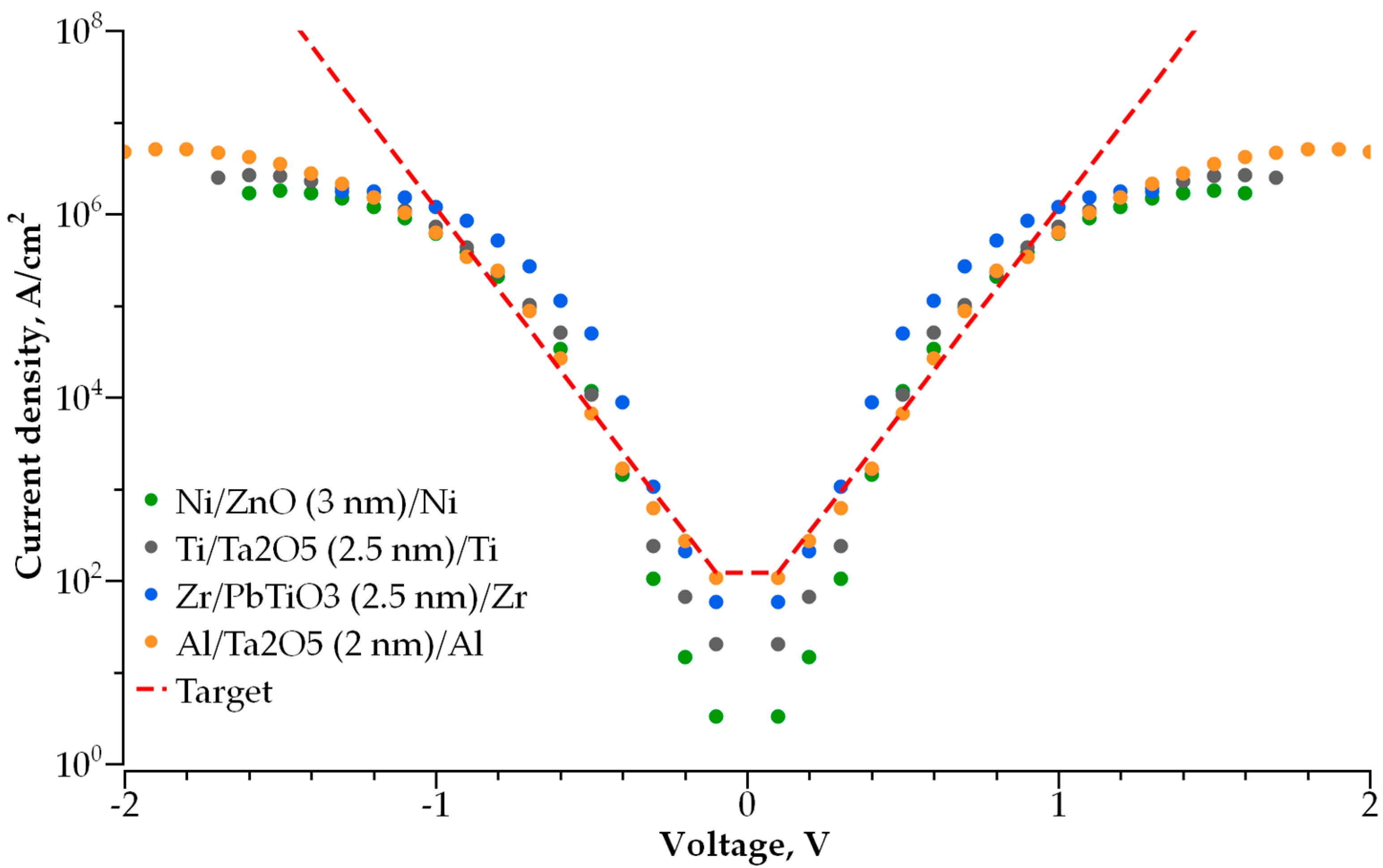
The current–voltage characteristics are diode-like [22], without hysteresis during forward and reverse voltage sweep; i.e., the selector material should be free of shallow and deep traps, which are able to capture and hold negative charge.
(2)
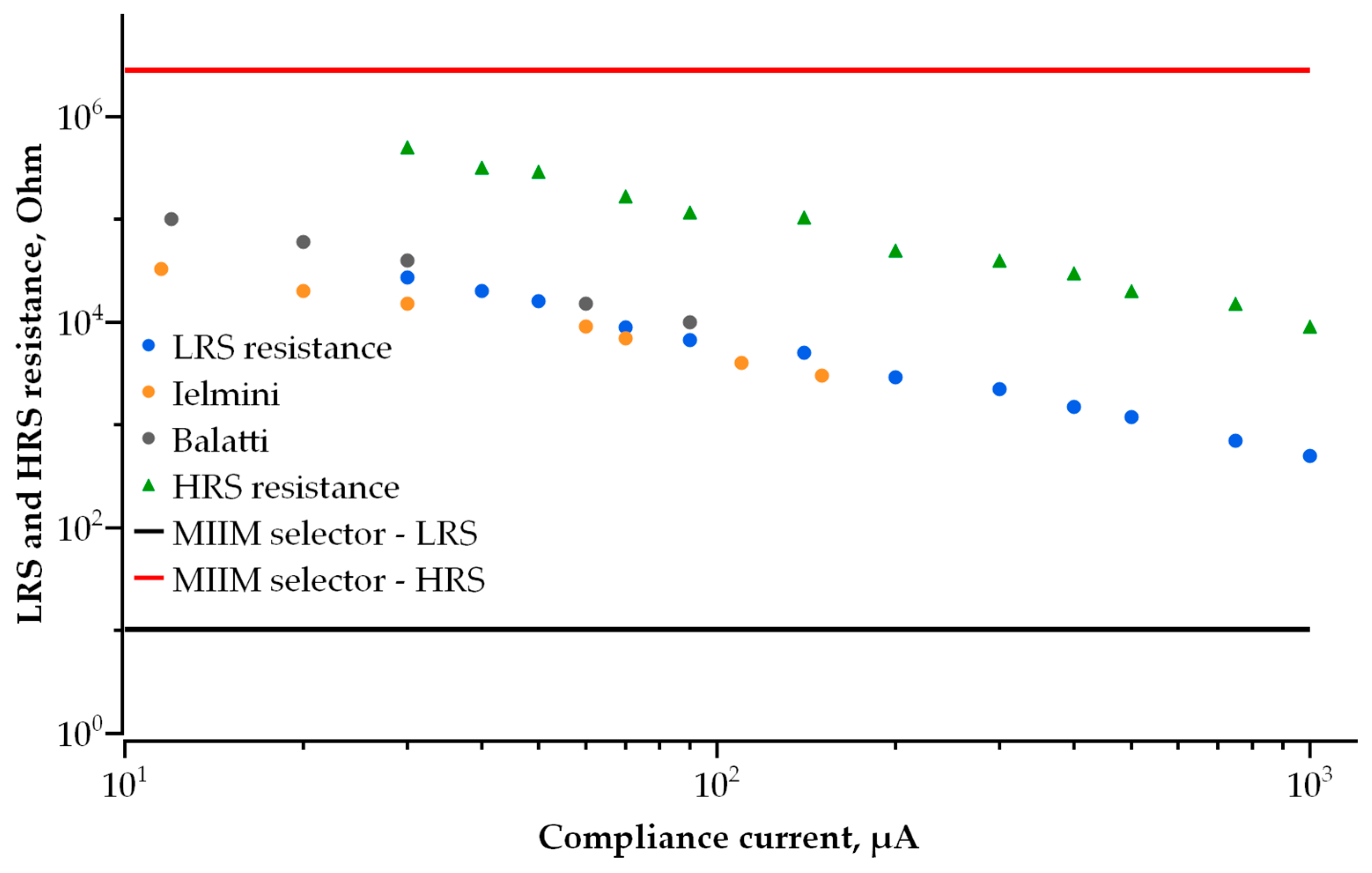
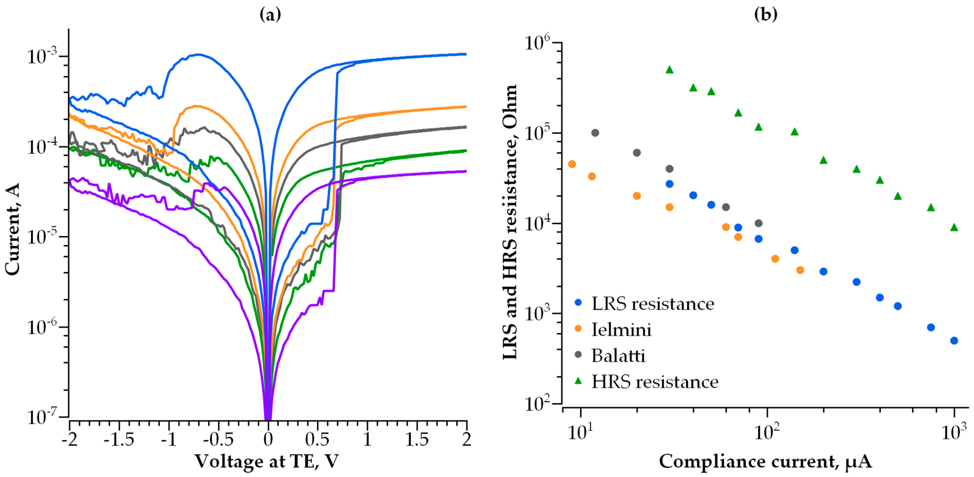
Selector resistance at a programming voltage (typically of 0.5 V to 1 V) should be in a range of 102 to 104 Ω, depending on the memory cell resistance in its low-resistance state (LRS) [23].
(3)
Selector resistance at a reading voltage (typically 0.1 V) should be in a range of 104 to 106 Ω, depending on the memory cell resistance in its high-resistance state (HRS) [24].
These requirements are based on the resistive switching characteristics of hafnium-oxide-based RRAM published in [7,10], as well as on our own experimentally measured resistive switching characteristics of the 1 transistor-1 resistor (1T1R) structures with a 10 nm thick HfOx film and TaN metal electrodes [35]. The HRS and LRS currents are extracted from the current–voltage characteristics of the RRAM elements (Figure 2a), measured at various values of the compliance current (Icompl) and controlled by the integrated field-effect transistor during the transition from HRS to LRS (Set). Both LRS and HRS currents increase with an increasing Icompl value. The LRS resistance as a function of the compliance current is presented in Figure 2b. The data for hafnium-oxide-based RRAM reported in [7,10] are also presented in Figure 2b for comparison. Thus, the data in Figure 2b define the current operation field for the selector to be used for hafnium-oxide-based RRAM. It should be noted that operation fields for other transition metal oxides are quite similar to that of hafnium oxide due to the filamentary nature of their resistive switching.
In addition to the compliance current that affects the HRS current, the maximum voltage used during the transition from LRS to HRS (Reset) can also control the HRS current. The switching characteristics obtained on the same device but with various values of the maximum Reset voltage are presented in Figure 3a. The dependence of the HRS current measured at a reading voltage of 0.1 V on the maximum Reset voltage is shown in Figure 3b.
During a programming step, the selector must not interfere with the transition of the memory cell to a low-resistance state. This implies that resistance is to be lower than the resistance of a memory cell at Set voltage. At the same time, during the reading operation, spontaneous switching of the cell from the high-resistance state (HRS) should not occur. The selector, in this case, should work as a reverse-biased diode, the resistance of which should be much greater than the resistance of the memory cell in the high-resistance state.
A physical model describing the conductivity in nanoscale dielectric structures is required to create an optimal self-aligned selector. The conductivity mechanism of selector based on MIM structure depends on the type of dielectric, its thickness and bandgap width. It can utilize Poole–Frenkel conductivity, Fowler–Nordheim tunneling [36], direct tunneling and trap-assisted tunneling [37]. It was demonstrated in [36] that several mechanisms can work simultaneously, e.g., the Poole–Frenkel and Fowler–Nordheim conductivity. The conductivity model can also vary depending on the magnitude of the voltage applied to the dielectric [36]. However, in most single-layer dielectrics with nanometer-scale thicknesses and voltages in the order of 1 V (typical writing voltage in RRAM), the main mechanism of conductivity derived by the Wentzel–Kramers–Brillouin (WKB) approximation [38] is a form of direct tunneling through a rectangular potential barrier (Figure 4, Equations (1) and (2)), which, at high voltages, smoothly transforms into Fowler–Nordheim tunneling (Equation (3)) [38]. This model is confirmed by both theoretical [39] and experimental [21,40] studies. Some additional possible conduction mechanisms, such as trap-assisted tunneling and Poole–Frenkel conduction, are out of the scope of this work, as they could be related to specific dielectric materials with electron traps, such as Al2O3 [36].
The potential barrier that exists between an electrode and a dielectric layer has two important parameters: the width, which equals the thickness of a corresponding dielectric layer, and height, that, in terms of energy, is equal to the difference between electron affinity of dielectric and work function of the electrode. In this study, we consider only the structures with metal electrodes made of the same material.
In case of a single-layer dielectric and for low voltages (V < φ), the WKB approximation [38] yields classical equation of direct tunneling:
J = J 0 ( ( φ e V 2 ) × exp ( A φ e V 2 ) ( φ + e V 2 ) × exp ( A φ + e V 2 ) )
where J is current density, φ is potential barrier height, e is electron charge, V is applied voltage and J0 and A are the following constants [38]:
J 0 = e 2 π h d 2   ; A = 4 π d 2 m h
where e is electron charge, h is Planck’s constant, d is dielectric thickness and m is electron’s effective mass.
For higher voltages (V > φ), the potential barrier shape is changed from rectangular to triangular [38], and the effective width of the barrier is reduced. In this case, the WKB approximation yields
J = 2.2 e 3 F 2 8 π h φ ( exp ( 8 π 2.96 h e F 2 m φ 3   ) ( 1 + 2 eV φ ) exp ( 8 π 2.96 h e F 2 m φ 3   ( 1 + 2 eV φ ) ) )
where electric F is field in dielectric. This equation describes the Fowler–Nordheim tunneling.
We used the WKB approximation to calculate conductivity of the step-shaped barriers in double-layer dielectric structures. Based on Simmons’ research [38], we calculated the direct tunneling equation for a bilayer structure with a step-shaped potential barrier (Figure 5).
In case of potential barrier that consists of several dielectric layers, the total tunneling probability is equal to product of tunneling probabilities through each layer. According to WKB approximation, the tunneling probability through i-th layer is identical to the case of single arbitrary-shaped barrier [38]:
P i = exp [ 2 2 m i 2 x i 1 x i U i ( x ) E d x ]
where xi−1 and xi are the boundaries of i-th layer, Ui is the shape of i-th barrier as a function of x, mi is electron’s effective mass in i-th layer and E is kinetic energy of incident electron. In our case of rectangular potential barrier,
U i ( x ) = φ i e V i x d i
where Vi is voltage drop in i-th layer, di is respective layer’s thickness and φi is the bottom energy of conduction band of i-th dielectric (Figure 6).
Vi/di in Equation (5) is equal to electric field Di in i-th layer and can be calculated as
D i = V i d i = V ε i * j = 1 i d j ε j
where εi is dielectric constant of i-th layer. Substituting (5) and (6) into (4) yields
P i = exp [ 4 ε i 2 m i * 2 × j = 1 i ( d j ε j ) 3 e V { ( U i e V i E ) 3 / 2 ( U i e V i + 1 E ) 3 / 2 } ]
where mi is electron effective mass in the i-th dielectric layer, Vi is voltage drop in the i-th layer, V is applied voltage, dj is thickness of each dielectric, εj is dielectric constant of a respective layer and E is kinetic energy of incident electron. Equation (7) is valid under the assumption that all dielectric layers are homogenous—the dielectric constant εj of j-th layer is the same across the bulk of the layer. The tunneling probabilities Pi depend on the voltage drop across each layer, the material’s dielectric constant and thickness of the layer:
P ( E ) = i P i ,
The total tunnel current density through the cell is determined by the difference (Equation (9)) between the forward flux (Equation (10)) caused by diffusion and the backward voltage-driven drift of electrons (Equation (11)).
J t o t a l = J f o r w a r d J b a c k w a r d ,
J f o r w a r d = m e 2 π 2 3 E f 0 P ( E ) E d E
J b a c k w a r d = m e 2 π 2 3 E f 0 P ( E ) ( E + e V ) d E
This method can be used for all types of multilayer tunnel structures, regardless of number of dielectric layers and with arbitrary dielectric parameters, assuming that all dielectrics are homogenous. However, Equation (7) gives a correct result only for voltages lower than the height of potential barrier (Ui > eVi). For higher voltages, the conductivity is dominated by the highest barrier in multilayer structure, and in this case, one should use Equation (3). In case of a single-layer rectangular barrier, the integration of (9) yields the well-known Simmons Formula (1) [38]. We neglected the effect of the image forces occurring in potential barrier for the sake of simplifying the calculations.

3. Results

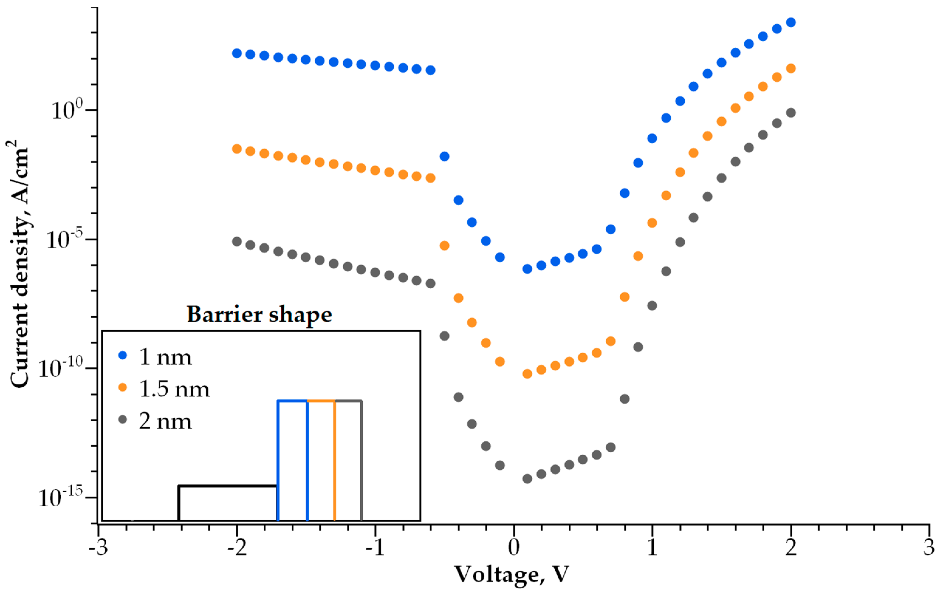
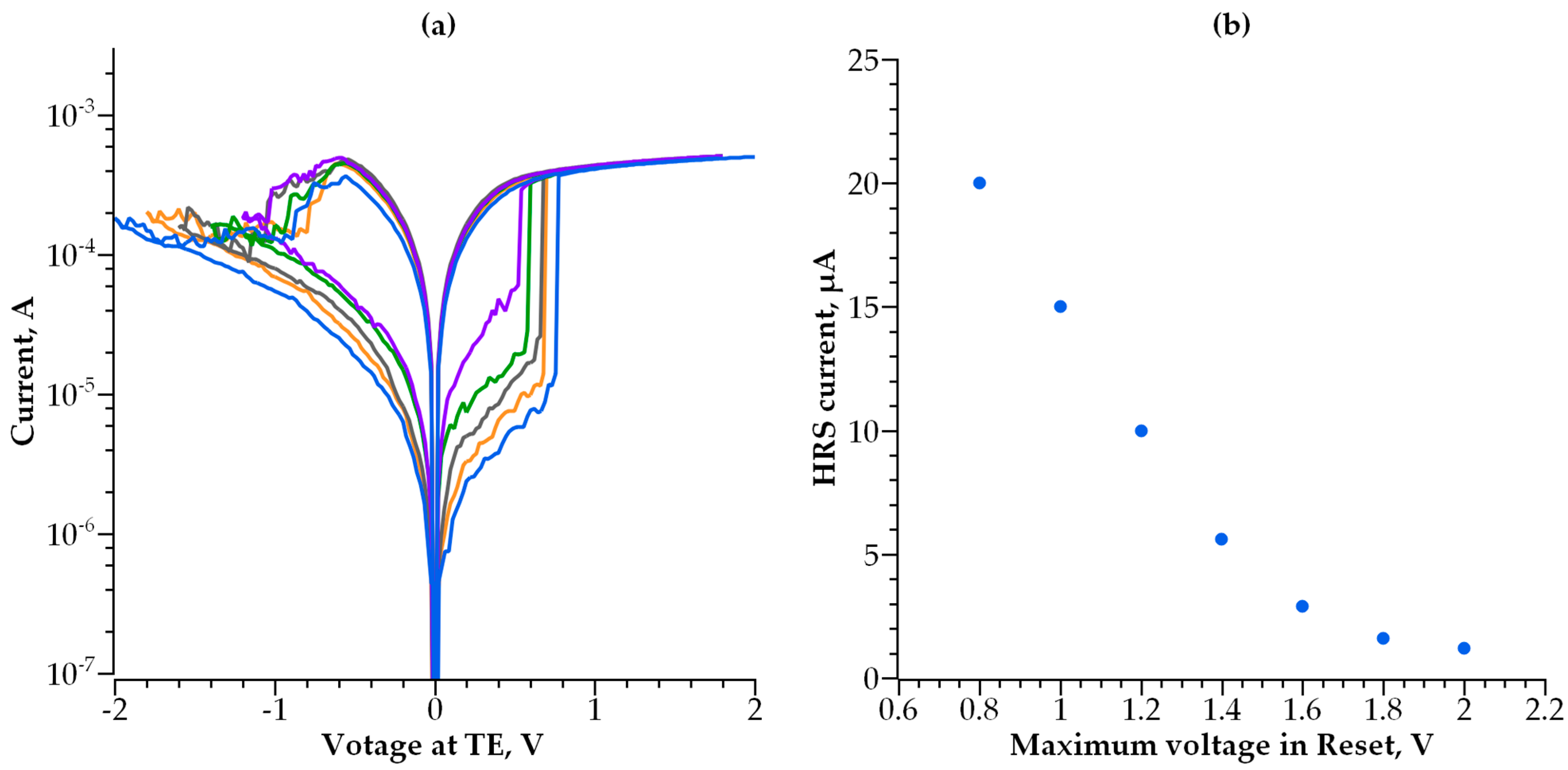
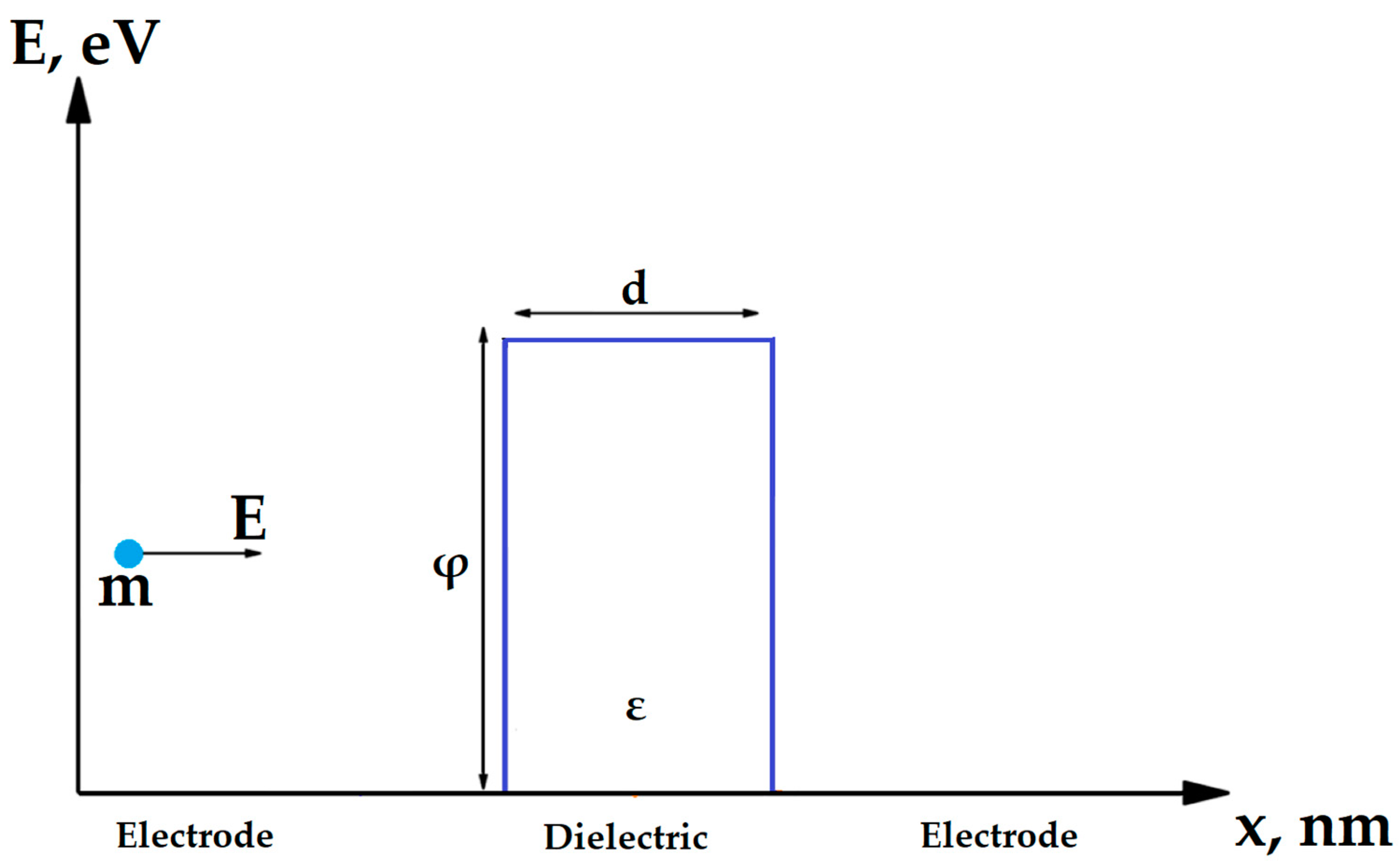
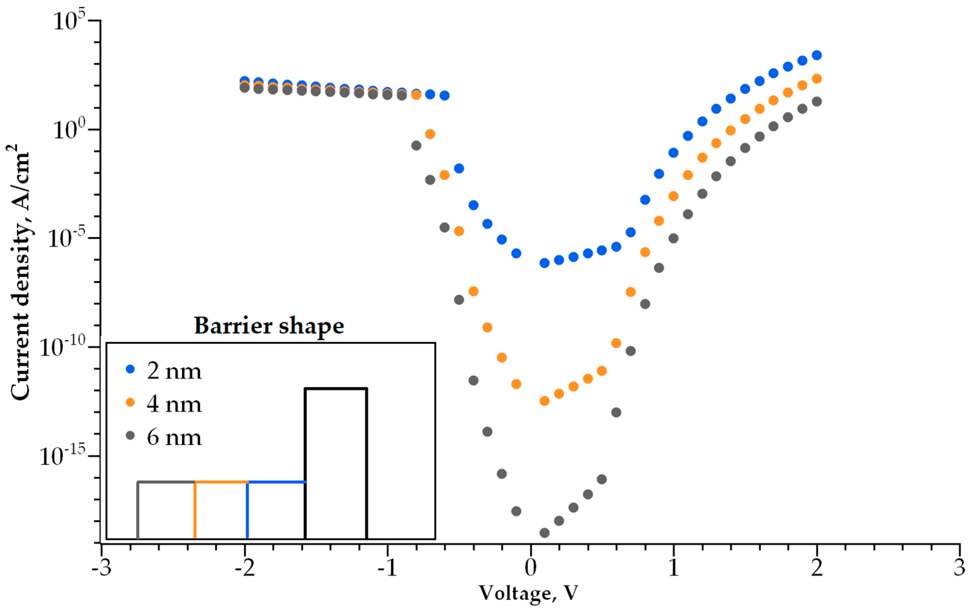
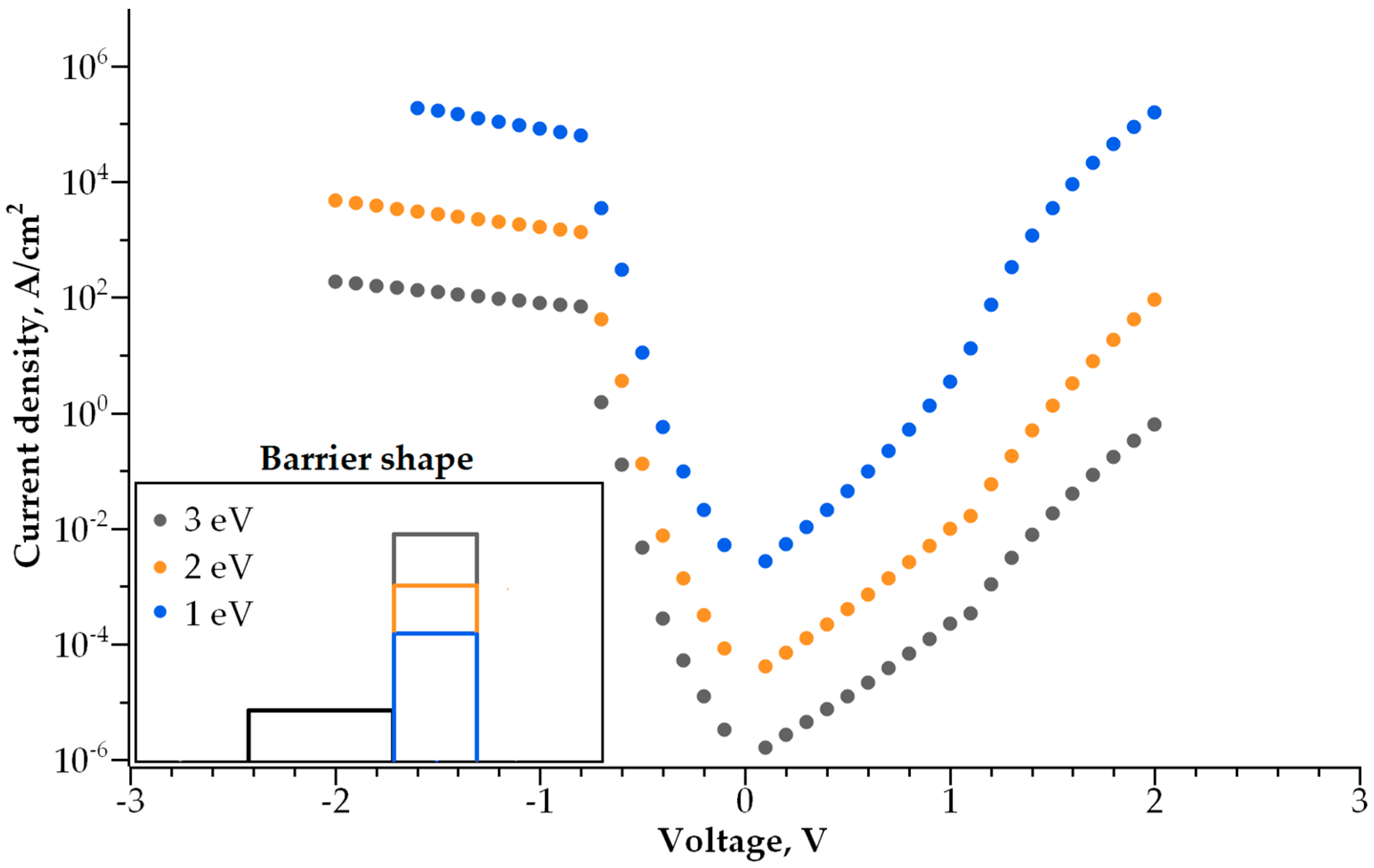
3.1. Single-Layer Selector

We simulated the I-V characteristics for dozens of single-layer dielectric structures with various electrode and dielectric materials. The best structures that meet the abovementioned requirements are presented in Figure 7. To verify the correctness of the employed model, we calculated the conductivity of the MIM selector based on the 2 nm thick Ta2O5 used in [21]. Figure 8 presents the experimentally measured [21] and calculated I-V characteristics of the ultra-thin tantalum-oxide-based selector. The comparison reveals good agreement for the measured and calculated currents in the −2 V to 2 V voltage range that covers the operating range for the selector.
According to the above-mentioned requirements for the selector, the steeper I-V curve results in better performance of the MIM selector. In Figure 8, the red dashed line represents the I-V characteristic of an optimal MIM selector with a minimal possible non-linearity and the current density in its open state. The stronger the current dependence on voltage and the higher the current density, the better the performance of the selector, and its size can be scaled down. We found that the desired characteristics of a selector are determined by the optimal values of height and width of a potential barrier between the electrode and dielectric (Figure 9a,b). Figure 9a shows the dependence of I-V curve non-linearity on the barrier’s height, while the thickness of the dielectric is fixed at 2 nm. The non-linearity of the I-V curve drops exponentially with an increase in barrier height. The thickness of the potential barrier affects the non-linearity in an opposite way. Figure 9b shows the dependence of I-V curve non-linearity on the barrier’s width (barrier height is fixed at 0.9 eV); an increase in dielectric layer thickness results in better non-linearity, which increases exponentially with barrier thickness. Therefore, a lower and thicker barrier results in a steeper I-V curve for selectors with a single-layer dielectric. In this case, the layer thickness cannot exceed 3 nm; otherwise, the current flowing through the selector in series with an RRAM cell is insufficient for the correct operation of the memory cell. The optimal barrier height for a 2 to 3 nm thick dielectric is found to be 0.3 to 0.5 eV. The materials presented in Figure 6 are the most satisfactory dielectrics to be used for self-aligned selectors.

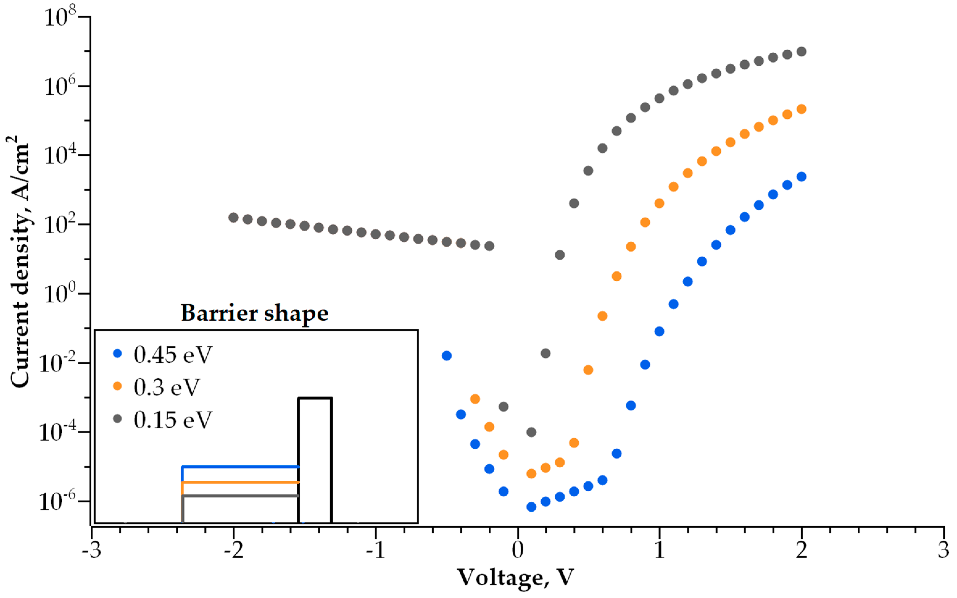
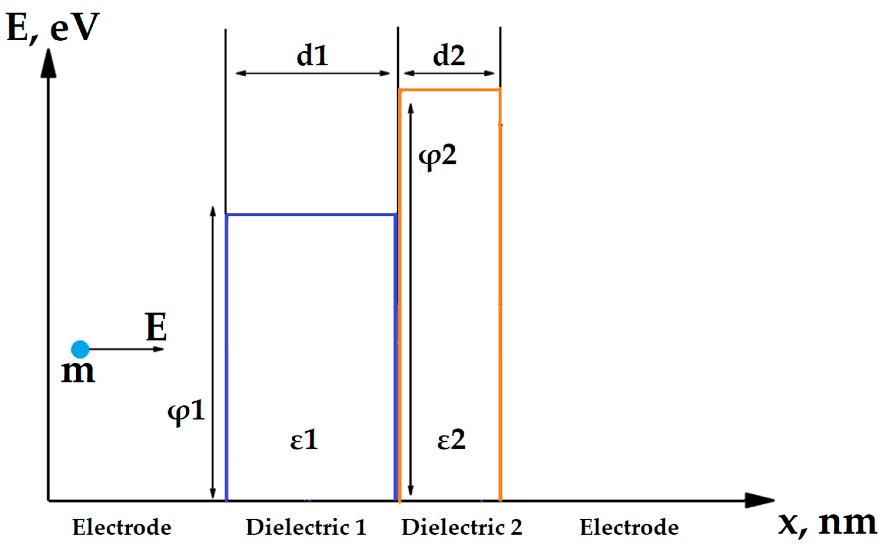
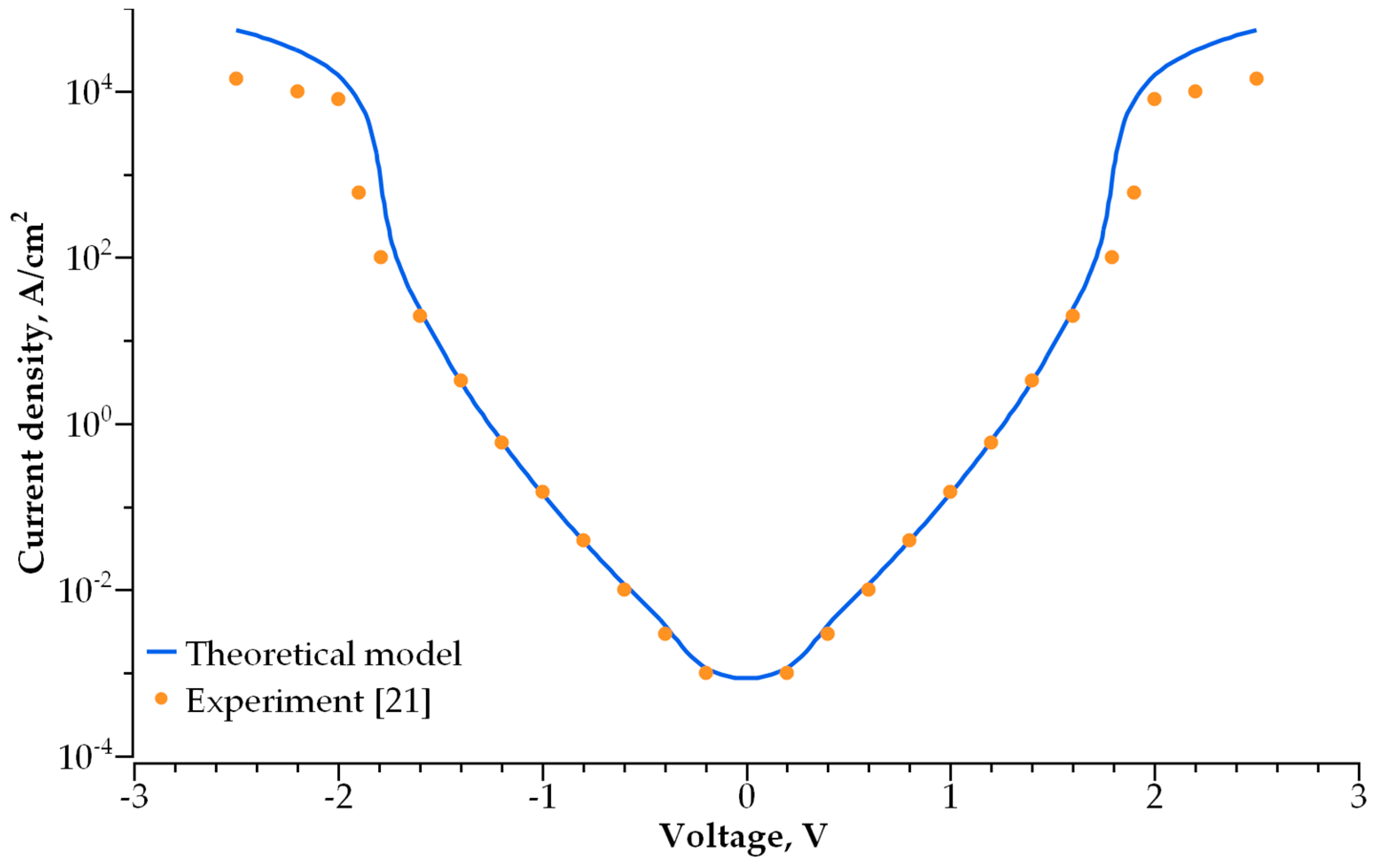
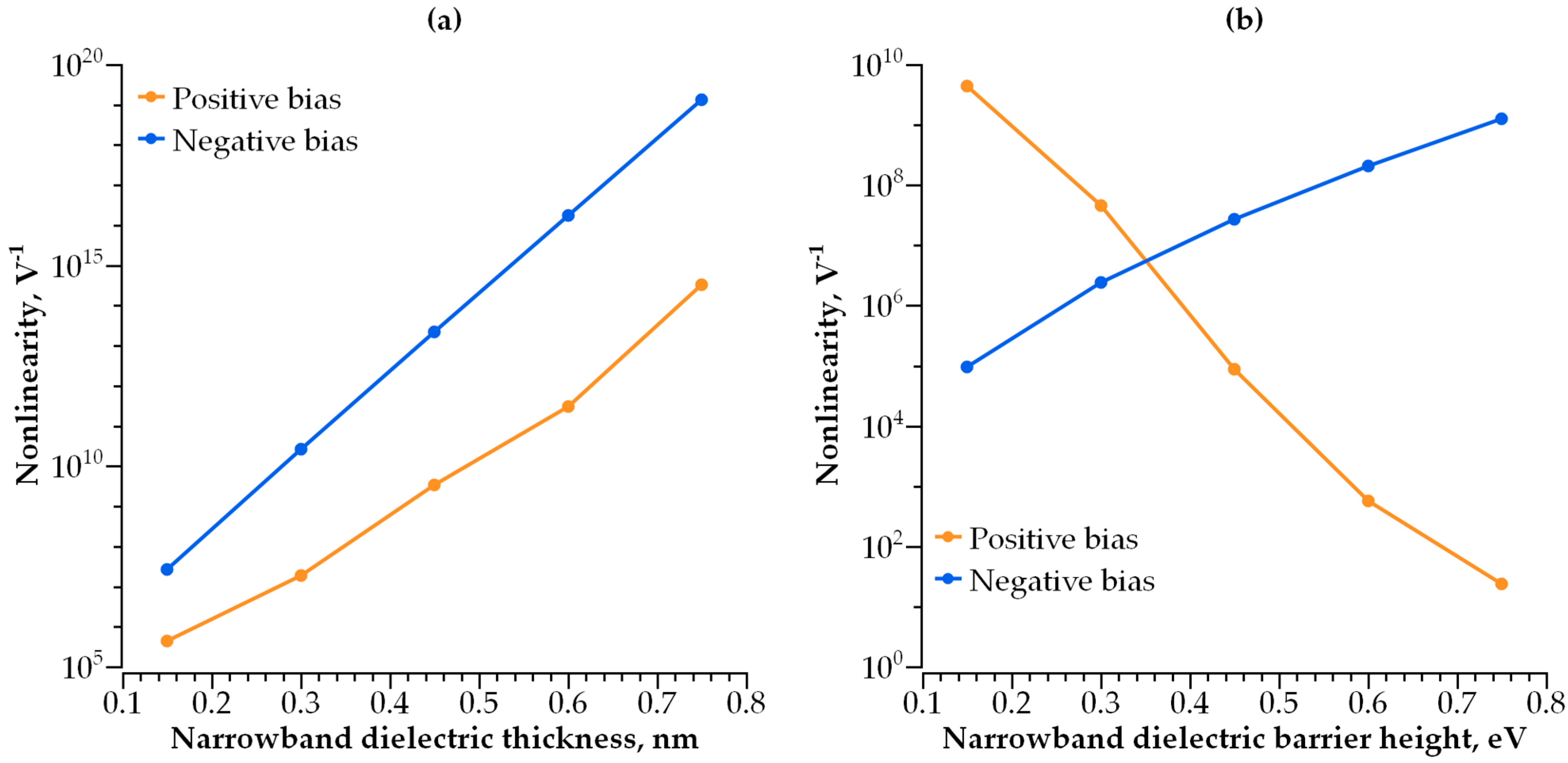
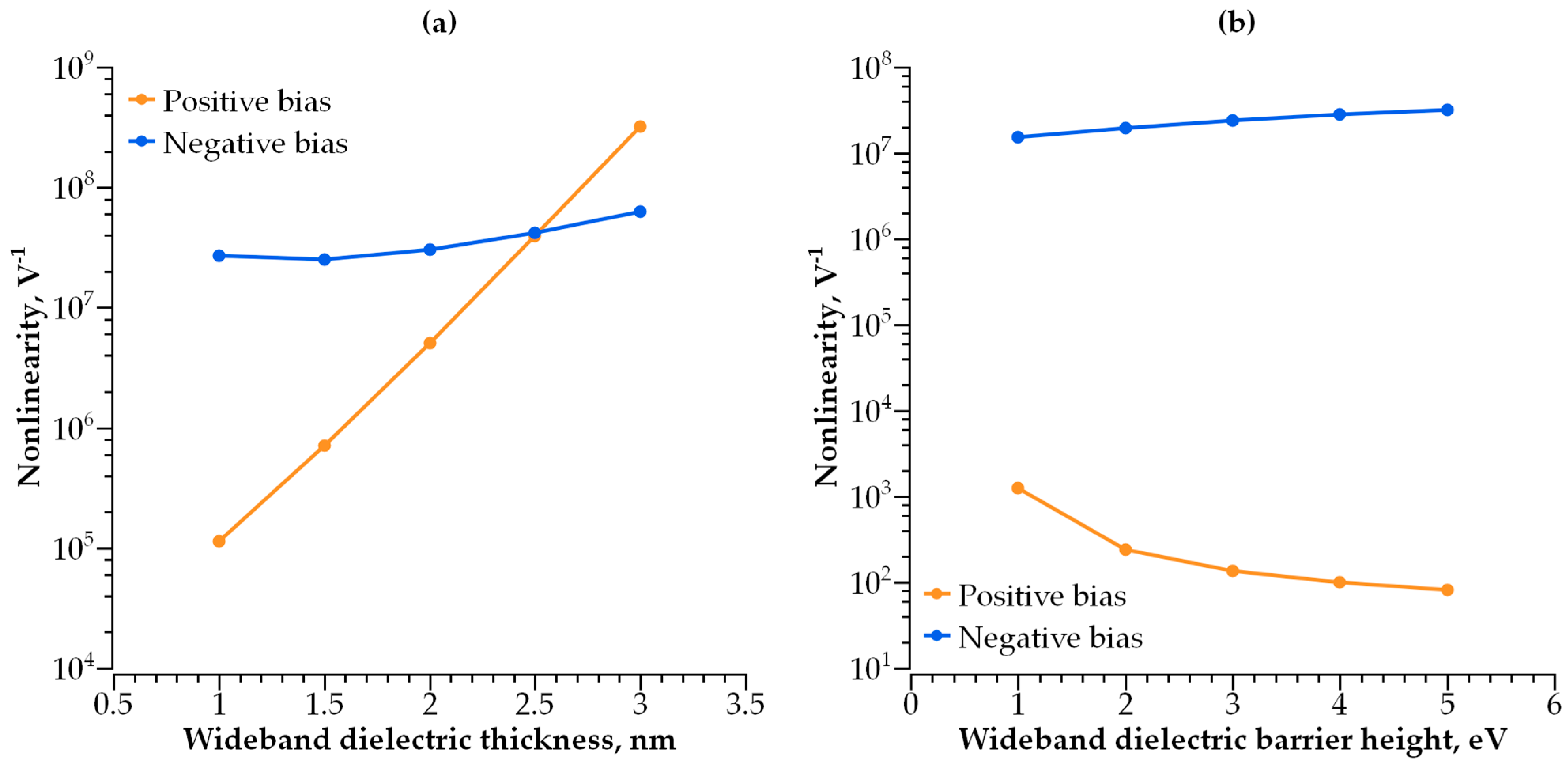
3.2. Double-Layer Selector

Adding a second dielectric layer makes further I-V curve modulation possible, i.e., increasing its non-linearity without a decrease in conductivity. The barrier becomes step-shaped, with a narrow-band dielectric acting as a lower step and a wide-band dielectric acting as a higher step. By varying the height and width of each step, one can control both the I-V curve steepness and current density independently. We studied how both parameters depend on the barrier geometry (Figure 10, Figure 11, Figure 12 and Figure 13).
The dependence of the I-V curve on the barrier geometry presented in Figure 10, Figure 11, Figure 12 and Figure 13 reveals clear trends for the I-V curve non-linearity and the current density at 1 V (a typical write voltage for RRAM cell). The non-linearity of the I-V characteristics depends primarily on the narrow-band dielectric width and the height of its potential barrier. The non-linearity increases rapidly with an increasing barrier thickness for both positive and negative biases (Figure 14a), while the non-linearity dependence on the barrier height is sensitive to the voltage polarity (Figure 14b). The non-linearity dependence on the width and height of a wide-band dielectric is not so strong, as compared to the effect of a narrow-band dielectric (Figure 15a,b).
The current density depends on the thickness and barrier height of both dielectric layers. The current density increases with decreasing layer thickness (Figure 16a) and reducing barrier height (Figure 16b). The key factors controlling the current density are wide-band dielectric thickness (Figure 16a) and narrow-band dielectric barrier height (Figure 16b). However, an increasing dielectric thickness and barrier height result in decreasing current density. This, in turn, negatively affects selector scalability, as the selector with a lower conductivity requires a larger area to be effective for the write operation.

4. Discussion

As shown above, the main mechanism of conductivity for thin dielectrics in a low electric field is direct tunneling through a rectangular potential barrier. In this case, the current flowing through the dielectric layer can be described by the WKB approximation [38]. At a higher voltage, when the shape of a potential barrier becomes triangle-like, the conductivity is followed by the Fowler–Nordheim tunneling mechanism. The feasibility of this approach is verified by calculating the I-V characteristics for the 2 nm thick Ta2O5 layer and comparison with the experimental results obtained in [21]. The calculations performed for a variety of sub-3 nm thick single-layer dielectrics demonstrated that some of them can be used for self-aligned selectors (Figure 7).
We developed a compact analytical model of conductivity in multilayer tunnel barriers and utilized it to study the switching operation of a self-aligned selector with a double-layer tunnel barrier. The observed I-V curve dependencies on the thickness and barrier heights of dielectrics for double-layer barriers are critical for the determination of the optimal structure of an MIIM-diode selector. By increasing the number of dielectric layers and their thickness, the selector non-linearity is enhanced at the cost of current density. Therefore, an optimal balance between non-linearity and conductivity is of the greatest importance. We also emphasize that the parameters of a self-aligned selector to be employed in RRAM Crossbars strongly depend on the parameters of the RRAM cell connected in series to a selector. The most critical parameter of an RRAM cell is its resistances in the on and off states, which can be controlled by either the maximum current during forming or Set operation (Figure 2) and/or the maximum voltage during Reset (Figure 3). Furthermore, RRAM resistance depends on the materials used for RRAM cells and the thickness of the corresponding switching layer. The parameters of an optimal selector we propose in this work are developed on the basis of our previous study [35] on HfOx-based bipolar RRAM cells with a 10 nm HfOx layer and TaN electrodes. The selector allowing a RRAM cell to operate during bipolar resistive switching consists of 1.5 nm layers of Ta2O5 and Ga2O3 sandwiched between Ti electrodes (Figure 17). The barrier heights in this structure are 0.05 eV and 0.6 eV, respectively. Because of its asymmetric structure and optimized thickness and barrier height for each dielectric layer, it has 10-times higher non-linearity for the I-V curve compared to the best single-layer selectors, as well as 10-times higher current density in the open state (Figure 17).
The advantages of a selector with double-layer dielectric allows for scaling the cell in a Crossbar HfOx-based RRAM array down to 103 μm2 (Figure 18). In Figure 18, the red line represents the resistance of the above-mentioned selector with double-layer dielectric in the high-resistance state at a voltage equal to 0.1 V, and the black line is the resistance of the same selector in the low-resistance state at a voltage equal to 1 V. The operating range of the selector with an area of 103 μm2 covers the entire operation range of RRAM cells paired to the selector. Thus, it becomes theoretically possible to create a gigabit-scale memory array in an area of 1 cm2, which is impossible when using a selector with a single-layer dielectric.

5. Summary and Conclusions

The strong scalability of an RRAM cell due to the filamentary mechanism of resistive switching is the key advantage for the development of a high-density Crossbar memory array. A selector device that is self-aligned with a memory cell makes Crossbar array scalability possible. In this work, we addressed the theoretical and modeling aspects of creating a self-aligned tunnel diode-based selector with optimal parameters to avoid impacts on the resistive switching of an HfOx-based RRAM cell. The applicability of both single- and double-layer dielectrics for self-aligned selectors was demonstrated along with the determination of their optimal physical properties. Aside from RRAM crossbars, the MIIM diode optimization method we propose is equally applicable for optical rectification purposes in renewable energy applications, where both high non-linearity and high current density are required [40], as well as for other THz devices and prospective tunnel diodes.
However, the primary field where our findings are useful is the self-aligned selector technology for RRAM Crossbars, because for each type of RRAM cell, an individual selector is designed based on the cell’s electrical properties. The non-volatile resistance switching phenomenon has been reported for a variety of oxides and metal electrode materials [4]. High-density arrays made on both types of RRAM devices with conductive filaments, i.e., oxygen vacancies’ filament-based RRAM [7,10,11,12,16] and metal ion-based RRAM (or conductive bridge random-access memory) [14,41,42], require a proper selector to eliminate the sneaking current issue while not interfering with the RRAM cell performance.
Thus, our work can be used as a template for other researchers seeking to create RRAM memory arrays with low power consumption and high storage density. These devices are crucial for next-generation computers and the creation of analog neuromorphic networks.

Author Contributions

Conceptualization, S.K.; methodology, S.K., V.K. and M.F.; formal analysis, S.K., V.K. and M.F.; investigation, M.F.; resources, S.K. and V.K.; data curation, M.F.; writing—original draft preparation, M.F.; writing—review and editing, S.K. and V.K.; visualization, M.F.; supervision, S.K.; project administration, S.K.; funding acquisition, S.K. All authors have read and agreed to the published version of the manuscript.

Funding

This work was carried out within the framework of the Russian Federation State Task No 075-00296-24-00.

Data Availability Statement

The data presented in this study are available on request from the corresponding author.

Conflicts of Interest

The authors declare no conflicts of interest. The funders had no role in the design of the study; in the collection, analyses, or interpretation of data; in the writing of the manuscript; or in the decision to publish the results.

References

  1. Waser, R.; Aono, M. Nanoionics-based resistive switching memories. Nat. Mater. 2007, 6, 833–840. [Google Scholar] [CrossRef] [PubMed]
  2. Yang, J.J.; Strukov, D.B.; Stewart, D.R. Memristive devices for computing. Nat. Nanotechnol. 2012, 8, 13–24. [Google Scholar] [CrossRef] [PubMed]
  3. Ding, X.; Feng, Y.H.; Jinfeng, K. Low-Power Resistive Switching Characteristic in HfO2/TiOx Bi-Layer Resistive Random-Access Memory. Nanoscale Res. Lett. 2019, 14, 157. [Google Scholar] [CrossRef] [PubMed]
  4. Zahoor, F.; Zulkifli, T.Z.A.; Khanday, F. Resistive Random Access Memory (RRAM): An Overview of Materials, Switching Mechanism, Performance, Multilevel Cell (mlc) Storage, Modeling, and Applications. Nanoscale Res. Lett. 2020, 15, 1–26. [Google Scholar] [CrossRef] [PubMed]
  5. Prezioso, M.; Merrikh-Bayat, F.; Hoskins, B.; Adam, G.C.; Likharev, K.K.; Strukov, D.B. Training and operation of an integrated neuromorphic network based on metal-oxide memristors. Nature 2015, 521, 61–64. [Google Scholar] [CrossRef] [PubMed]
  6. Wan, W.; Kubendran, R.; Schaefer, C.; Eryilmaz, S.B.; Zhang, W.; Wu, D.; Deiss, S.; Raina, P.; Qian, H.; Gao, B.; et al. A compute-in-memory chip based on resistive random-access memory. Nature 2022, 608, 504–512. [Google Scholar] [CrossRef]
  7. Ambrogio, S.; Balatti, S.; Cubeta, A.; Calderoni, A.; Ramaswamy, N.; Ielmini, D. Statistical Fluctuations in HfOx Resistive-Switching Memory: Part I—Set/Reset Variability. IEEE Trans. Electron. Dev. 2014, 61, 2912–2919. [Google Scholar] [CrossRef]
  8. Ho, C.; Hsu, C.-L.; Chen, C.-C.; Liu, J.-T.; Wu, C.-S.; Huang, C.-C.; Hu, C.; Yang, F.-L. 9 nm Half-Pitch Functional Resistive Memory Cell with <1 μA Programming Current Using Thermally Oxidized Sub-Stoichiometric WOx Film. In Proceedings of the IEEE International Electron Devices Meeting (IEDM), San Francisco, CA, USA, 6–8 December 2010; pp. 19.1.1–19.1.4. [Google Scholar]
  9. Lu, Y.; Lee, J.H.; Chen, I.-W. Scalability of Voltage-Controlled Filamentary and Na-nometallic Resistance Memories. Nanoscale 2017, 9, 12690–12697. [Google Scholar] [CrossRef] [PubMed]
  10. Balatti, S.; Ambrogio, S.; Ielmini, D.; Gilmer, D.C. Variability and failure of set process in HfO2 RRAM. In 2013 5th IEEE International Memory Workshop; IEEE: Piscataway, NJ, USA, 2013; pp. 38–41. [Google Scholar]
  11. Bousoulas, P.; Stathopoulos, S.; Tsialoukis, D.; Tsoukalas, D. Low-power and highly uniform 3-b multilevel switching in forming free TiO2-x-based RRAM with embedded Pt nanocrystals. IEEE Electron. Device Lett. 2016, 37, 874–877. [Google Scholar] [CrossRef]
  12. Chen, S.X.; Chang, S.P.; Chang, S.J.; Hsieh, W.K.; Lin, C.H. Highly stable ultrathin TiO2-based resistive random access memory with low operation voltage. ECS J. Solid State Sci. Technol. 2018, 7, Q3183. [Google Scholar] [CrossRef]
  13. Maikap, J. Dutta Self-compliance RRAM characteristics using a novel W/TaOx/TiN structure. Nanoscale Res. Lett. 2014, 9, 292. [Google Scholar] [CrossRef]
  14. Chung, Y.L.; Cheng, W.H.; Jeng, J.S.; Chen, W.C.; Jhan, S.A.; Chen, J.S. Joint contributions of Ag ions and oxygen vacancies to conducting filament evolution of Ag/TaOx/Pt memory device. J. Appl. Phys. 2014, 116, 164502. [Google Scholar] [CrossRef]
  15. Li, Y.; Long, S.; Zhang, M.; Liu, Q.; Shao, L.; Zhang, S.; Wang, Y.; Zuo, Q.; Liu, S.; Liu, M.; et al. Resistive switching properties of Au/ZrO2/Ag structure for low-voltage nonvolatile memory applications. IEEE Electron. Device Lett. 2009, 31, 117–119. [Google Scholar]
  16. Wang, S.Y.; Lee, D.Y.; Tseng, T.Y.; Lin, C.Y. Effects of Ti top electrode thickness on the resistive switching behaviors of rf-sputtered ZrO2 memory films. Appl. Phys. Lett. 2009, 95, 112904. [Google Scholar] [CrossRef]
  17. Baek, I.G.; Lee, M.S.; Seo, S.; Lee, M.J.; Seo, D.H.; Suh, D.S.; Park, J.C.; Park, S.O.; Kim, H.S.; Yoo, I.K.; et al. Highly scalable non-volatile resistive memory using simple binary oxide driven by asymmetric unipolar voltage pulses. In Technical Digest—International Electron Devices Meeting; IEEE: Piscataway, NJ, USA, 2004; pp. 587–590. [Google Scholar]
  18. Ielmini, D. Brain-inspired computing with resistive switching memory (RRAM): Devices, synapses and neural networks. Microelectron. Eng. 2018, 190, 44–53. [Google Scholar] [CrossRef]
  19. Xia, L.; Gu, P.; Li, B.; Tang, T.; Yin, X.; Huangfu, W.; Tu, S.; Cao, Y.; Wang, Y.; Yang, H. Technological Exploration of RRAM Crossbar Array for Matrix-Vector Multiplication. J. Comput. Sci. Technol. 2016, 31, 3–19. [Google Scholar] [CrossRef]
  20. Flocke, A.; Noll, T.G. Fundamental analysis of resistive nanocrossbars for the use in hybrid nano/CMOS-memory. In Proceedings of the 33rd ESSCIRC, Munich, Germany, 11–13 September 2007. [Google Scholar]
  21. Govoreanu, B.; Adelmann, C.; Redolfi, A.; Zhang, L.; Clima, S.; Jurczak, M. High-Performance Metal-Insulator-Metal Tunnel Diode Selectors. IEEE Electron. Device Lett. 2014, 35, 63–65. [Google Scholar] [CrossRef]
  22. Lin, C.; Li, G.; Jia, X. Resistance requirements of threshold switching selectors in 1S1R crossbar array. In Proceedings of the 2017 International Conference on Electronic Information Technology and Computer Engineering, Zhuhai, China, 22–24 September 2017. [Google Scholar]
  23. Kim, S.; Zhou, J.; Lu, W.D. Crossbar RRAM Arrays: Selector Device Requirements During Write Operation. IEEE Trans. Electron Devices 2014, 61, 2820–2826. [Google Scholar]
  24. Zhou, J.; Kim, K.-H.; Lu, W. Crossbar RRAM Arrays: Selector Device Requirements During Read Operation. IEEE Trans. Electron. Devices 2014, 61, 1369–1376. [Google Scholar] [CrossRef]
  25. Lee, M.J.; Kim, S.I.; Lee, C.B.; Yin, H.; Ahn, S.E.; Kang, B.S.; Kim, K.H.; Park, J.C.; Kim, C.J.; Song, I.; et al. Low-temperature-grown transition metal oxide based storage materials and oxide transistors for high-density non-volatile memory. Adv. Funct. Mater. 2008, 19, 1587–1593. [Google Scholar] [CrossRef]
  26. Huang, J.-J.; Tseng, Y.-M.; Hsu, C.W.; Hou, T.H. Bipolar nonlinear Ni/TiO2/Ni selector for 1S1R crossbar array applications. IEEE Electron. Device Lett. 2011, 32, 1427–1429. [Google Scholar] [CrossRef]
  27. Shin, J.; Kim, I.; Biju, K.; Jo, M.; Park, J.; Lee, J.; Jung, S.; Lee, W.; Kim, S.; Park, S.; et al. TiO2-based metal-insulator-metal selection device for bipolar resistive random access memory cross-point application. J. Appl. Phys. 2011, 109, 712. [Google Scholar] [CrossRef]
  28. Lee, W.; Park, J.; Shin, J.; Woo, J.; Kim, S.; Choi, G.; Jung, S.; Park, S.; Lee, D.; Cha, E.; et al. Varistor-type bidirectional switch (JMAX > 107A/cm2, selectivity 104) for 3D bipolar resistive memory arrays. In Proceedings of the 2012 Symposium on VLSI Technology (VLSIT), Honolulu, HI, USA, 12–14 June 2012. [Google Scholar]
  29. Gopalakrishnan, K.; Shenoy, R.S.; Rettner, C.T.; Virwani, K.; Bethune, D.S.; Shelby, R.M.; Burr, G.W.; Kellock, A.; King, R.S.; Nguyen, K.; et al. Highly-scalable novel access device based on mixed ionic conduction (MIEC) materials for high density phase change memory (PCM) array. In Proceedings of the 2010 Symposium on VLSI Technology (VLSIT), Honolulu, HI, USA, 15–17 June 2010. [Google Scholar]
  30. Srinivasan, V.S.S.; Chopra, S.; Karkare, P.; Bafna, P.; Lashkare, S.; Kumbhare, P.; Kim, Y.; Srinivasan, S.; Kuppurao, S.; Lodha, S.; et al. Punchthrough-Diode-Based Bipolar RRAM Selector by Si Epitaxy. IEEE Electron Device Lett. 2012, 33, 1396–1398. [Google Scholar] [CrossRef]
  31. Kwon, W.; Jeon, J.; Hutin, L.; Liu, T.-J.K. Electromechanical Diode Cell for Cross-Point Nonvolatile Memory Arrays. IEEE Electron. Device Lett. 2011, 33, 131–133. [Google Scholar] [CrossRef]
  32. Li, Y.; Fu, L.; Tao, C.; Jiang, X.; Sun, P. Feasibility study of using a Zener diode as the selection device for bipolar RRAM and WORM memory arrays. J. Phys. D Appl. Phys. 2013, 47, 25103. [Google Scholar] [CrossRef]
  33. Diaz Leon, J.J.; Norris, K.J.; Yang, J.J.; Sevic, J.F.; Kobayashi, N. A niobium oxide-tantalum oxide selector-memristor self-aligned nanostack. Appl. Phys. Lett. 2017, 110, 103102. [Google Scholar] [CrossRef]
  34. Wang, X.P.; Fang, Z.; Li, X.; Chen, B.; Gao, B.; Kang, J.F.; Kwong, D.L. Highly compact 1T-1R architecture (4F2 footprint) involving fully CMOS compatible vertical GAA nano-pillar transistors and oxide-based RRAM cells exhibiting excellent NVM properties and ultra-low power operation. In Proceedings of the 2012 International Electron Devices Meeting, San Francisco, CA, USA, 10–13 December 2012; pp. 20.6.1–20.6.4. [Google Scholar] [CrossRef]
  35. Fedotov, M.I.; Korotitsky, V.I.; Koveshnikov, S.V. Experimental and Theoretical Study of Intrinsic Variability in Hafnium Oxide Based RRAM. In Proceedings of the IEEE 22nd International Conference of Young Professionals in Electron Devices and Materials (EDM), Souzga, Russia, 30 June–4 July 2021. [Google Scholar]
  36. Vaziri, S.; Belete, M.; Litta, E.D.; Smith, A.D.; Lupina, G.; Lemme, M.C.; Östling, M. Bilayer insulator tunnel barriers for graphene-based vertical hot-electron transistors. Nanoscale 2015, 7, 13096–13104. [Google Scholar] [CrossRef] [PubMed]
  37. Hansen, M.; Ziegler, M.; Kolberg, L.; Soni, R.; Dirkmann, S.; Mussenbrock, T.; Kohlstedt, H. A double barrier memristive device. Sci. Rep. 2015, 5, 13753. [Google Scholar] [CrossRef] [PubMed]
  38. Simmons, J.G. Generalized Formula for the Electric Tunnel Effect between Similar Electrodes Separated by a Thin Insulating Film. J. Appl. Phys. 1963, 34, 1793–1803. [Google Scholar] [CrossRef]
  39. Jagath, A.L.; Kumar, T.N.; Almurib, H.A.; Jinesh, K.B.P. Analytical modelling of tantalum/titanium oxide-based multi-layer selector to eliminate sneak path current in RRAM arrays. IET Circuits Devices Syst. 2020, 14, 1092–1098. [Google Scholar] [CrossRef]
  40. Matsuura, D.; Shimizu, M.; Yugami, H. High-current density and high-asymmetry MIIM diode based on oxygen-non-stoichiometry controlled homointerface structure for optical rectenna. Sci. Rep. 2019, 9, 19639. [Google Scholar] [CrossRef] [PubMed]
  41. Valov, I.; Waser, R.; Jameson, J.R.; Kozicki, M.N. Electrochemical metallization memories—Fundamentals, applications, prospects. Nanotechnology 2011, 22, 254003. [Google Scholar] [CrossRef] [PubMed]
  42. Tian, Q.; Zhang, X.; Zhao, X.; Wang, Z.; Lin, Y.; Xu, H.; Liu, Y. Dual Buffer Layers for Developing Electrochemical Metallization Memory with Low Current and High Endurance. IEEE Electron Device Lett. 2020, 42, 308–311. [Google Scholar] [CrossRef]
Figure 1. Three-electrode RRAM Crossbar with self-aligned selectors. Area of selector is equal to area of RRAM cell.
Nanomaterials 14 00668 g001
Figure 2. (a) Switching characteristics of HfOx-based RRAM obtained on the same device at various values of compliance current; (b) LRS and HRS resistance measured at a read voltage of 0.1 V as a function of compliance current, compared to [7,10].
Nanomaterials 14 00668 g002
Figure 3. (a) Switching characteristics of HfOx-based RRAM obtained on the same device at various values of maximum voltage in Reset; (b) HRS current measured at a read voltage of 0.1 V as a function of maximum voltage in Reset.
Nanomaterials 14 00668 g003
Figure 4. Band diagram of a tunnel diode selector with a single-layer dielectric.
Nanomaterials 14 00668 g004
Figure 5. Band diagram of a tunnel diode selector with a double-layer dielectric.
Nanomaterials 14 00668 g005
Figure 6. Band diagram of multilayer tunnel barrier under applied voltage.
Nanomaterials 14 00668 g006
Figure 7. Simulated I-V curves of best single-layer (MIM) selector devices. Red dashed line is desired I-V curve.
Nanomaterials 14 00668 g007
Figure 8. Comparison of the experimental [21] and modelled I-V characteristics for 2 nm thick Ta2O5 with a barrier height of 0.9 eV.
Nanomaterials 14 00668 g008
Figure 9. (a) I-V curve non-linearity dependence on barrier height, d = 2 nm; (b) I-V curve non-linearity dependence on barrier thickness, φ = 0.9 eV.
Nanomaterials 14 00668 g009
Figure 10. I-V curves for various thicknesses of narrowband dielectric layer. Inset shows the barrier shape.
Nanomaterials 14 00668 g010
Figure 11. I-V curves for various thicknesses of wideband dielectric layer. Inset shows the barrier shape.
Nanomaterials 14 00668 g011
Figure 12. I-V curves for various barrier heights of the narrowband dielectric layer. Inset shows the barrier shape.
Nanomaterials 14 00668 g012
Figure 13. I-V curves for various barrier heights of the wideband dielectric layer. Inset shows the barrier shape.
Nanomaterials 14 00668 g013
Figure 14. (a) I-V curve non-linearity dependence on narrow-band dielectric thickness; (b) I-V curve non-linearity dependence on barrier height of narrow-band dielectric.
Nanomaterials 14 00668 g014
Figure 15. (a) I-V curve non-linearity dependence on wide-band dielectric thickness; (b) I-V curve non-linearity dependence on barrier height of wide-band dielectric.
Nanomaterials 14 00668 g015
Figure 16. (a) Dependence of current density at 1 V on the dielectric thickness; (b) current density at 1V dependency on the dielectric barrier height.
Nanomaterials 14 00668 g016
Figure 17. I-V curve of double-layer selector (green dotted line) compared to the best single-layer selectors.
Nanomaterials 14 00668 g017
Figure 18. LRS and HRS resistance of double-layer selector device at 1 V and 0.1 V, respectively, as compared to LRS and HRS resistance of RRAM cell.
Nanomaterials 14 00668 g018
Disclaimer/Publisher’s Note: The statements, opinions and data contained in all publications are solely those of the individual author(s) and contributor(s) and not of MDPI and/or the editor(s). MDPI and/or the editor(s) disclaim responsibility for any injury to people or property resulting from any ideas, methods, instructions or products referred to in the content.

