1. Introduction
Due to a high surface-area-to-volume ratio and up to centimeter-scale lateral dimension, 2D materials are ideal for integration with current nanofabrication technologies and highly promising transduction materials in sensor technologies that rely primarily on surface interaction [
1]. A prominent example of functional 2D nanomaterials is graphene, which was the first 2D material isolated from its bulk structure in 2004 and has been extensively investigated. Despite its extraordinary properties, such as high optical transparency, thermal conductivity up to 3000 W m
−1 K
−1, high charge carrier concentration, and mobility [
2], the lack of an energy gap between the conduction and valence bands limits its application in electronic devices. Attempts to address this deficiency have led to several approaches to engineer a bandgap in graphene. However, most of the successful methods require lengthy and complicated processes of fabrication using e-beam lithography or unstable doping treatment with harsh chemicals [
3,
4]. These intensive processes often lead to a significant decrease in carrier mobility and an increase in the number of defects in graphene. This challenge has encouraged researchers to find alternative 2D materials, and transition metal dichalcogenides (TMDCs) have become an emerging field of research. Unlike graphene, TMDCs possess a direct bandgap in the range of 0.2 to 3 eV in their single-layer (SL) structure [
5]. This intrinsic band gap suggests that TMDCs are suitable for electronic/transistor applications. Molybdenum disulfide (MoS
2) is one of the most studied TMDC compounds. It consists of one layer of molybdenum atoms in between two layers of sulfur atoms. SL-MoS
2 exhibits a direct bandgap of 1.87 eV, which transitions to an indirect bandgap as the number of layers increase. Therefore, a field-effect transistor (FET) using SL-MoS
2 as a semiconducting channel is expected to have a high on/off current ratio of up to 10
8 and excellent subthreshold swing of 74 mV/decade [
6]. In addition, due to a planar structure confined to a few angstroms thickness, MoS
2 is ultrasensitive to chemical and electrostatic perturbations at the surface. These advantages make MoS
2 a great choice for transduction or sensing material in FET-based biosensors.
In the field of biosensor research, label-free affinity-based biosensing is a desirable attribute for biosensor systems due to its simplicity. Amongst the different transducers used for label-free affinity biosensors, FETs and chemiresistors based on 1D and 2D nanomaterials are receiving a great deal of attention because of their high sensitivity, rapid response, low power consumption, viability for miniaturization, scalability, and integration on a chip. While methods of electrical detection either with an applied gate (FET characteristic measurement) or without an applied gate (chemiresistive measurement) have been demonstrated for biosensors using semi-metallic graphene, semiconducting graphene derivatives and carbon nanotubes [
7,
8,
9,
10], MoS
2-based electrical biosensors heavily rely on FET techniques, in which a source-drain current (I
ds) is measured at a constant bias while varying the applied gate voltage to modulate the I
ds. This mandatory gate voltage serves as an amplifier of the small current by enhancing the carrier mobility, originated by the nature of low charge mobility in semiconducting MoS
2 and high Schottky barrier at the interface of MoS
2/metal contact [
11,
12]. In addition, because the applied back-gating effect plays a key role in FET-based measurement, it requires a reliable and direct physical contact between MoS
2 (the conducting channel) and the dielectric substrate. Nonuniform and unstable contact at the materials interface can result in unreliable electrical modulation via gating effects, further leading to degradation of signal integrity and reliability during sensing.
A necessary step in the fabrication of a label-free MoS
2-based biosensors is the immobilization of a biomolecular receptor to the surface of MoS
2 to achieve biospecific responses. This biofunctionalization step is achievable via covalent and non-covalent conjugation strategies, such as hydrophobic interaction, silanization, and sulfide/disulfide bonding [
13,
14,
15]. However, these methods either employ weak van der Waals bonds or significantly rely on the number of defects in MoS
2, which mainly comprises sulfur vacancies, to create such attachments. As a result, MoS
2-based biosensors are commonly fabricated using MoS
2 synthesized via chemical/physical exfoliation or hydrothermal reaction. MoS
2 synthesized via these methods produce a great number of defects permitting the direct functionalization of biomolecular receptors. On the other hand, biosensing applications using MoS
2 grown by chemical vapor deposition (CVD) are relatively limited due to an inadequate number of the defect sites in CVD-grown MoS
2 (CVD-MoS
2) crystal lattice. Despite this hinderance, CVD-MoS
2 exhibits a higher crystallinity and is amenable to mass production. For these reasons, CVD-MoS
2 deserves more attention in research for biological and chemical sensing applications.
In this work, we report a systematic investigation to identify causes of signal instability of CVD-MoS2 FET-based biosensors and develop a strategy to mitigate the effects of physical degradation of the device and enhance the overall device stability. Specifically, we observed that CVD-MoS2-based biosensors degraded, indicated by dramatic change in their electrical outputs during mandatory incubation steps of the biofunctionalization process in 10 mM phosphate buffer (pH = 7.4) and deionized water (pH = 7). We conclude the observed continual shifts in device FET characteristics was attributed to physical delamination of MoS2 film from Si/SiO2 substrate, which decreased the gating effect and negated the usage of FET characteristic transfer curve as a mean for detection. This issue was mitigated by stabilizing the device with a 30 nm thick Al2O3 coating. In addition, the oxide layer provided available sites for antibody functionalization via surface chemical functionalization with (3-aminopropyl) triethoxysilane (APTES) and glutaraldehyde. Such sensors demonstrated a great performance to detect HIgG with high sensitivity and a limit of detection of 83 ng/mL.
3. Results and Discussion
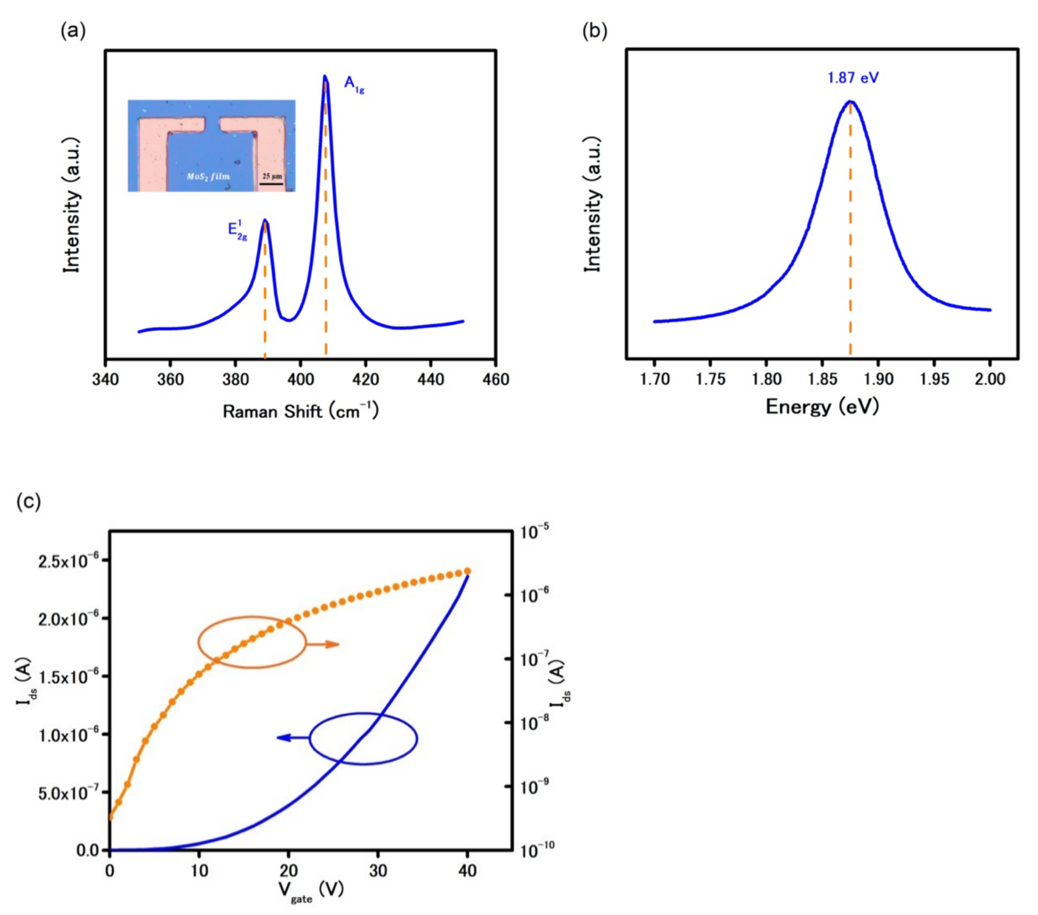
The optical image in
Figure 1a (inset) shows the MoS
2 synthesized by CVD was a continuous film that remained a continuous film after the transfer. The similarity of color contrast across the film illustrates the growth of MoS
2 was uniform and the transfer was residue-free.
The film thickness and electrical bandgap of the synthesized MoS
2 were confirmed by different techniques such as Raman spectroscopy, photoluminescence (PL) under a green laser with spot size ≈ 1 µm. The presence of two signature peaks of E
2g at 385 cm
−1 and A
1g at 404 cm
−1 in
Figure 1a confirms the successful growth of MoS
2. In addition, the difference in wavenumber of 19 cm
−1 between the two peaks indicates the as-grown MoS
2 was single-layer [
16]. Due to the intrinsic direct bandgap in SL MoS
2 structure, the photoluminescence spectrum in
Figure 1b shows a significantly high peak at 1.87 eV.
A back-gated FET using CVD-MoS
2 as the semiconducting channel was prepared using conventional photolithography process. As shown in
Figure 1c, the FET characteristics curve shows a typical n-type behavior with a high on/off current ratio of 10
4 in ambient condition. Under the applied positive back-gate voltage, the device was turned on, i.e., dramatic increase in current due to the accumulation of electrons in MoS
2. The field-effect mobility was calculated to be 20.5 cm
2V
−1s
−1, using the linear FET characteristics reported elsewhere [
17]. This low charge mobility is mainly caused by charge trapping at the interface between the SiO
2 substrate and MoS
2 [
18,
19] and high contact resistance at metal/MoS
2 interface [
11]. Because of such challenges, electrical measurement methods in MoS
2-based devices are limited to a FET characteristics curve with applied gate voltage [
13,
20,
21].
Due to the significant role of the FET measurement in MoS
2-based sensors, the stability of as-fabricated FET devices becomes critical. A stability test was carried out initially in ambient air and later in both biocompatible media of phosphate buffer (PB, pH = 7.4) and DI water (pH = 7). As shown in
Figure 2, the FET characteristics curve experienced a measurable decrease in current after 30 min in ambient air, which was due to the interaction between MoS
2 film and oxidizing gas molecules in air [
22]. However, after 30 min and for an additional 90 min under the same condition, the FET characteristics curve remained unchanged, which indicates physical and chemical pseudo-steady-state in the device.
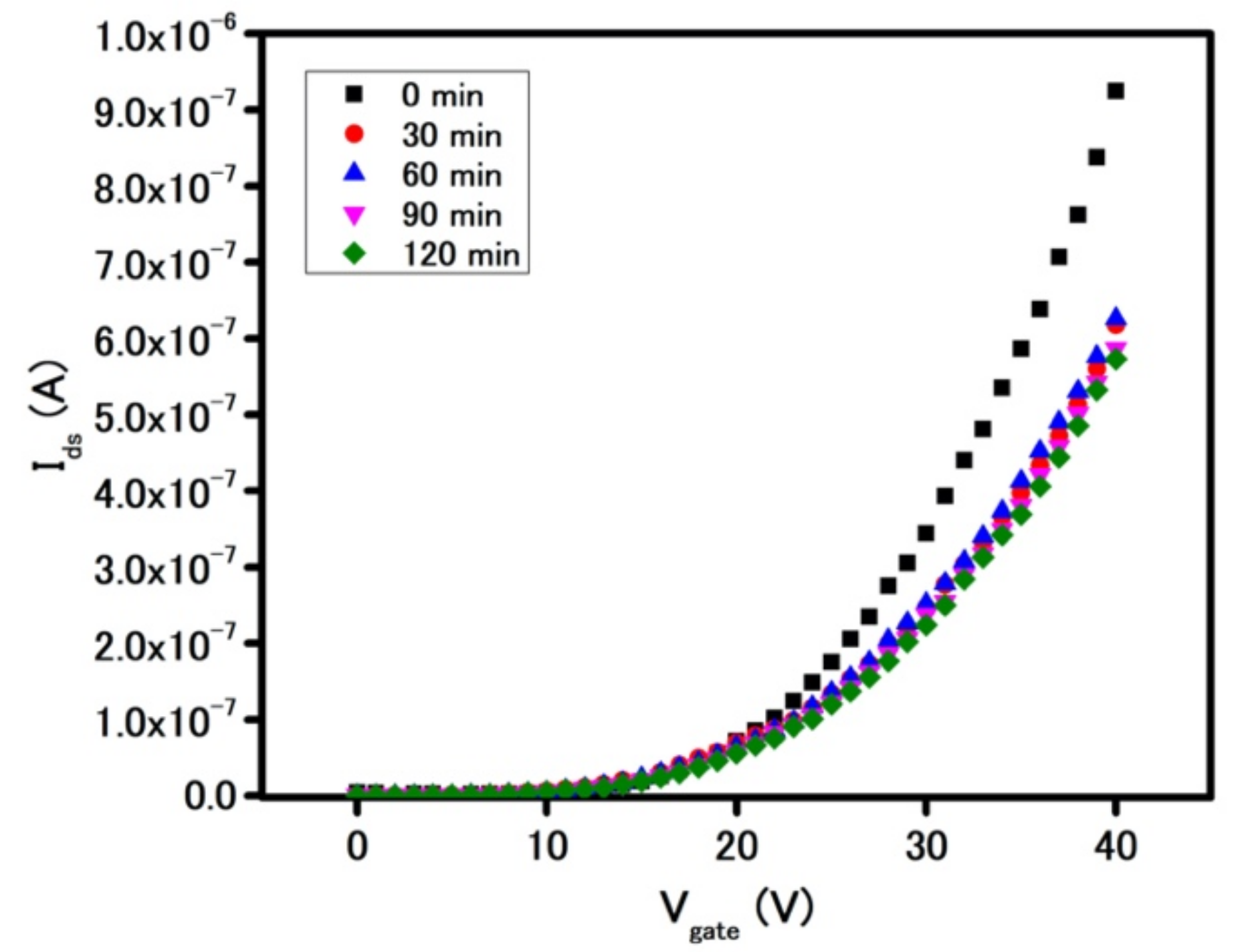
On the other hand, upon incubation in PB for 30 min by drop casting of 20 µL of PB onto the sensing area, the device showed a significant decrease in overall I
ds current across the entire range of applied gate voltages as seen in
Figure 3a. In fact, the current at the gate voltage of 40 V dropped by 33% after 30 min of incubation, as compared to further 1.6–5% drop after additional 90 min. Similar deterioration in electrical behavior was observed when the device was incubated in DI water (
Figure 3b). Thus, in considering the similar magnitudes of diminution of I
ds current for the device in the ionic PB environment and deionized water environment, this suggests the presence of water molecules as the major contributing factor for the observed electrical behavior of the device, instead of the buffer salt ions. Three possible mechanisms for how water could diminish the performance of a FET MoS
2-based device were considered:
Water altered the chemical properties of MoS2 during the incubation via -O or -OH bonding;
Water intercalated between gold electrodes and MoS2 and increased the contact resistance;
Water intercalated between MoS2 and the substrate and decreased the gating effect on the MoS2 channel.
Raman spectrometry was employed to examine the properties of MoS
2 after 30 min incubation in DI water [
23]. As illustrated in
Figure S1, the absolute intensity of the two signature peaks of MoS
2 remained unaffected after the incubation, indicating there was no oxidation taking place. As a result, the mechanism (1) of water induced chemical effect on MoS
2 film was disregarded.
To determine if the phenomenon of water intercalation between MoS
2 and gold electrodes was occurring, controlled experiments were conducted where MoS
2-electrode interfacial regions of the FET device were physically isolated (via passivation with photoresist) from the immediate buffer environment. A thin layer of positive photoresist S1813 was spin-coated on top of the device, and a small photoresist area of 10 μm × 10 μm at the contact between MoS
2 and gold electrodes was removed using photolithographic patterning. An optical image of such a schematic can be found in
Figure S2a. This polymeric layer behaved as a hydrophobic layer that prevented water from intercalating between the gold contacts and MoS
2 but still allowed the possibility of water inserting between MoS
2 film and Si/SiO
2 substrate due to the open window of 10 μm × 10 μm.
Figure S2b shows the resulting FET characteristic curves of pre-photoresist, post-photoresist, and after device incubation from 30 to 120 min in DI water. As a protecting layer, S1813 film minimized the interaction between MoS
2 and oxidizing gas molecules in the ambient, such as O
2 and water vapor, and thus increased the electrical outputs of FET devices as observed by the increase in the FET current. Similar FET transfer curves collected after 30, 60, 90 and 120 min indicates the device was more stable than the one without the photoresist but still suffered from the previously observed degradation. Therefore, this experiment series removed the possibility of mechanism (2) of the resistance increasing due to water intercalating between gold and MoS
2 and confirmed mechanism (3), i.e., water intercalated between conducting channel and the Si/SiO
2 substrate causing the delamination of MoS
2 film. This resulting poor contact between MoS
2 and the dielectric SiO
2 layer decreased the gating effect onto the conducting channel in FET measurement, yielding the false positive response in detection. In fact, the delamination phenomenon is a commonly used method for isolating CVD-grown MoS
2 from its growth substrate. Due to the high hydrophobicity of the substrate and MoS
2, water is used as a medium for a clean, complete lift-off for MoS
2 as reported elsewhere [
24,
25].
Even though the as-synthesized MoS
2 appeared as a continuous film as shown in
Figure 1a, it is believed that the film consisted of many single MoS
2 crystals with distinct grain boundaries. Therefore, further investigation on grain boundaries of the as-grown CVD-MoS
2 was conducted to understand in more depth the delamination phenomenon that resulted in the instability of MoS
2-based device. Work function of a similar CVD-SL-MoS
2 was measured at 4.90 eV in our previous work [
8] while the absolute potential of Au
3+/Au is 5.64 eV. The difference in the work functions creates an intrinsic internal force driving electrons from n-type MoS
2 to Au
3+ ions and reduced the ions to Au nanoparticles (NPs). This reduction happens at the reactive sites on MoS
2’s lattice, which concentrates at its edge and grain boundaries [
26,
27,
28] and, hence, MoS
2 grain boundaries become evidently detectable due the presence of formation of gold NPs.
Figure S3 shows scanning electron microscopic (SEM) images taken at the same location before and after an incubation of MoS
2 in 5.9 mM AuCl
3 solution for 10 min. The grain boundaries that were indistinguishable originally became evident due to the formation of Au NPs. This indicates the as-grown continuous MoS
2 film, in fact, consisted of many coalescing MoS
2 crystals. These existing large grain boundaries permitted water molecules to severely penetrate through MoS
2 film and delaminate it from the substrate.
This finding suggests that a physical passivation layer is required to minimize the intercalation of water molecules through MoS
2 grain boundaries leading to delamination of MoS
2 in aqueous solutions. Although a hydrophobic polymeric layer such as S1813 proved to alleviate the degradation of the FET device characteristics, its chemical inertness to surface chemical modification inhibits the subsequent biofunctionalization. On the other hand, thin metal oxide layers, such as hafnium oxide, silicon oxide, and aluminum oxide, are more commonly used as passive layers in logic electronics to protect the underneath material from being oxidized in the ambient [
29,
30]. In addition, the oxide layer, in presence of ambient and/or water vapor, produced sufficient hydroxyl groups making the device’s surface amenable for biofunctionalization. In this work, the aluminum oxide layer was deposited on the sensors using an ALD method [
31]. This deposition process involved two steps, in which the first step provided hydroxyl seeding by casting water vapor on the device‘s surface while the second step was a chemical reaction between -OH groups and TMA to form the Al
2O
3 layer. The schematic of MoS
2-based FETs with a Al
2O
3 passive layer is shown in
Figure S4.
Figure S5 shows the different color contrast of a device before and after Al
2O
3 deposition confirming the successful deposition of an oxide layer on the device. The thickness of the Al
2O
3 layer on the SiO
2 substrate was measured at 30 nm by ellipsometer, which can be found in
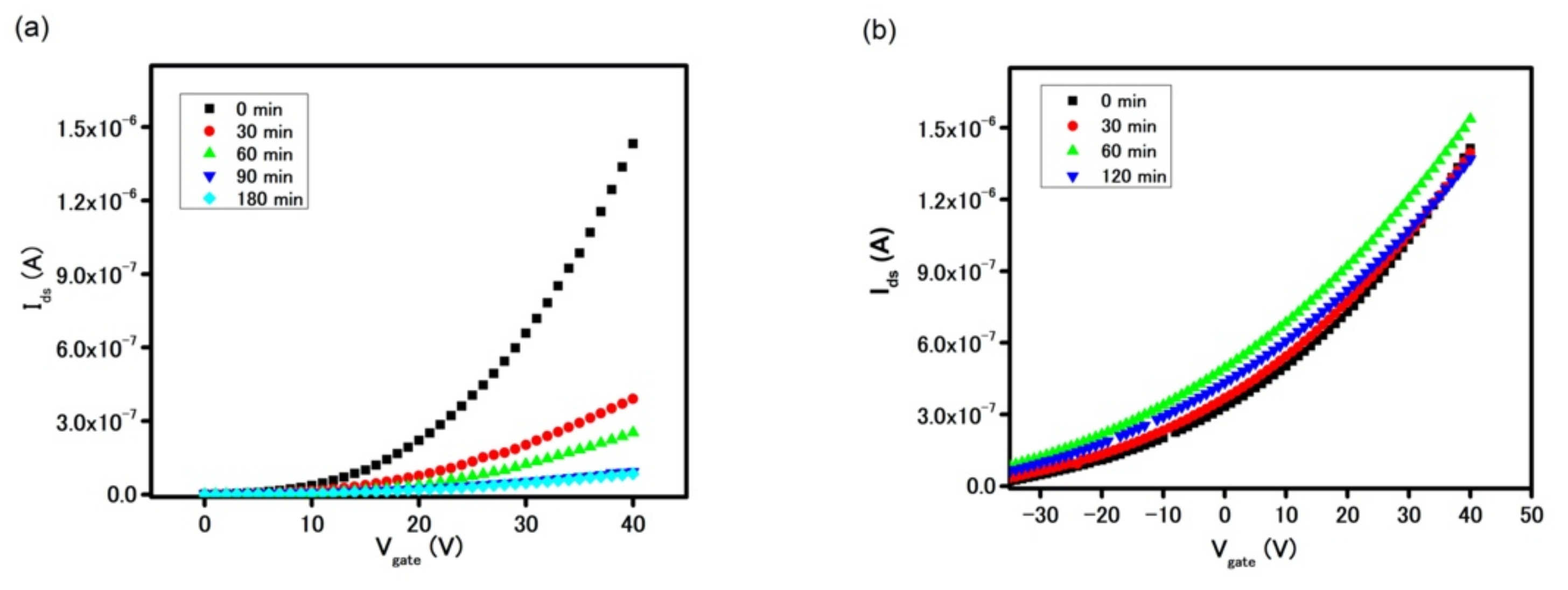
Figure S5c. The oxide layer’s thickness was optimized by measuring the device’s stability after incubation in DI water.
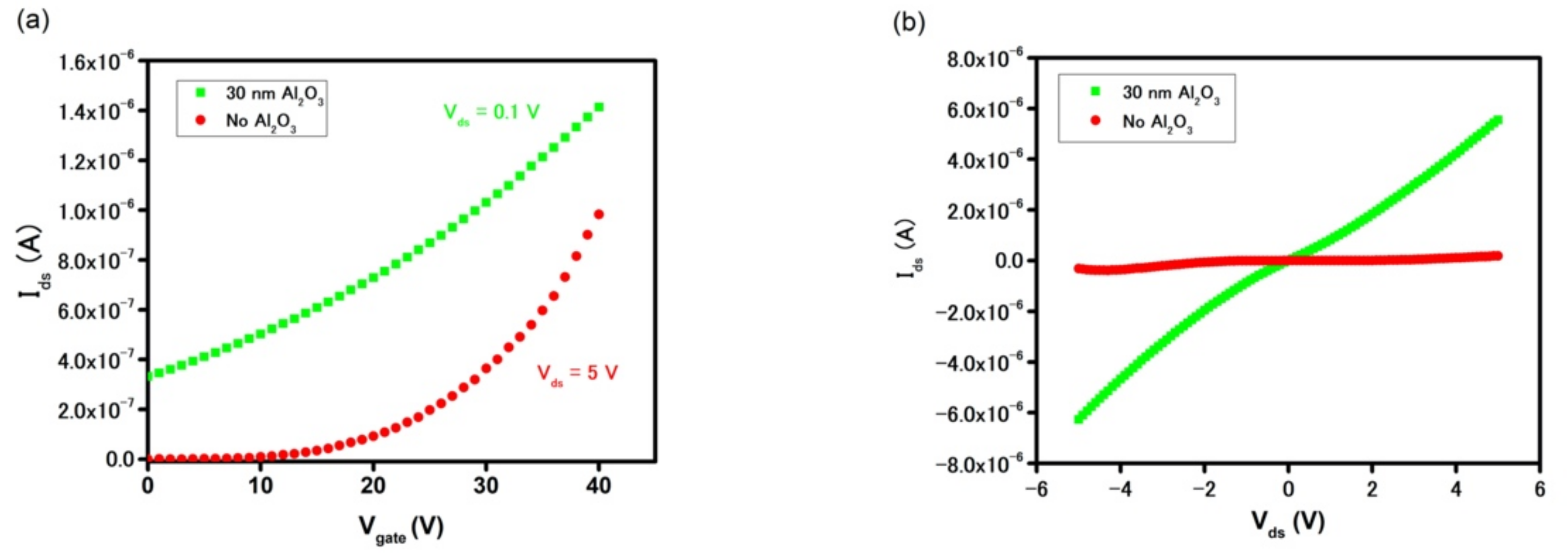
Figure 4 demonstrates a device with a 10 nm thick Al
2O
3 layer suffered from the degradation. On the other hand, the delamination phenomenon subsided in the device coated with a 30 nm thick oxide layer, as proven by the stable FET transfer curve of the device after 120 min. It is important to highlight that a strong n-doping effect of Al
2O
3 onto MoS
2 was also noticed in the FET and drain current measurements, as seen in
Figure 5 [
32,
33]. Due to its intrinsic semiconducting properties and relatively large work function, CVD-MoS
2 exhibits low charge mobility and the high contact resistance at MoS
2/gold interface. However, when the device was passivated by Al
2O
3 film, the insignificant current of 3 × 10
−10 A at V
gate = 0 V was increased by three orders of magnitude to 3 × 10
−7 A, while the field-effect charge mobilities increased by 26-fold, from 14 cm
2V
−1s
−1 to 367 cm
2V
−1s
−1 in the as-grown MoS
2 and Al
2O
3-MoS
2, respectively.
Figure 5a indicates the threshold voltage (V
TH) of the device also shifted to a more negative threshold voltage (V
TH) indicating a strong n-doping effect in MoS
2 by Al
2O
3. This interesting observation renders two possible reasons, including the incomplete oxidation of Al
2O
3 and the passivation of sulfur vacancy defects. During the Al
2O
3 growth, the incomplete reaction between TMA and water vapor resulted in excess positive charged Al
n+ ions. The residual positive charges in the oxide layer, hence, attracted additional electrons in the MoS
2 channel and promoted the n-doping effect. This led to the appreciable current found in the Al
2O
3 passivated device at V
gate = 0 V. On the other hand, as-grown CVD-MoS
2 exhibited a great number of sulfur vacancies at the boundaries and edges, as observed in the previous experiment with gold chloride solution. These vacancies created deep and localized states trapping electrons and, hence, impaired electron mobility in MoS
2 [
34,
35]. However, the presence of the Al
2O
3 layer allowed its oxygen atoms to fill sulfur vacancies and, in turn, minimized electrons trapping. Such a healing mechanism has been reported previously using other chemicals such as CO, NO, NO
2, and other sulfonate groups [
35,
36]. To the benefit of device electrical performance, this resulting increase in current and charge mobility provided additional electrical measurement method with less power consumption (no gate and lower V
ds) and simpler fabrication and operation due to the elimination of the gate.
Figure 5b highlights such an increase in drain current in the gateless FET device with an Al
2O
3 passive layer. At V
gate = 0 V, the I
ds current is as high as 9.2 × 10
−7 A at V
ds = 1 V and 5.6 × 10
−6 A at V
ds = 5 V (with Al
2O
3), as compared to 7.1 × 10
−10 A and 1.8 × 10
−7 A (without Al
2O
3), respectively.
As hydroxyl groups were available on the Al
2O
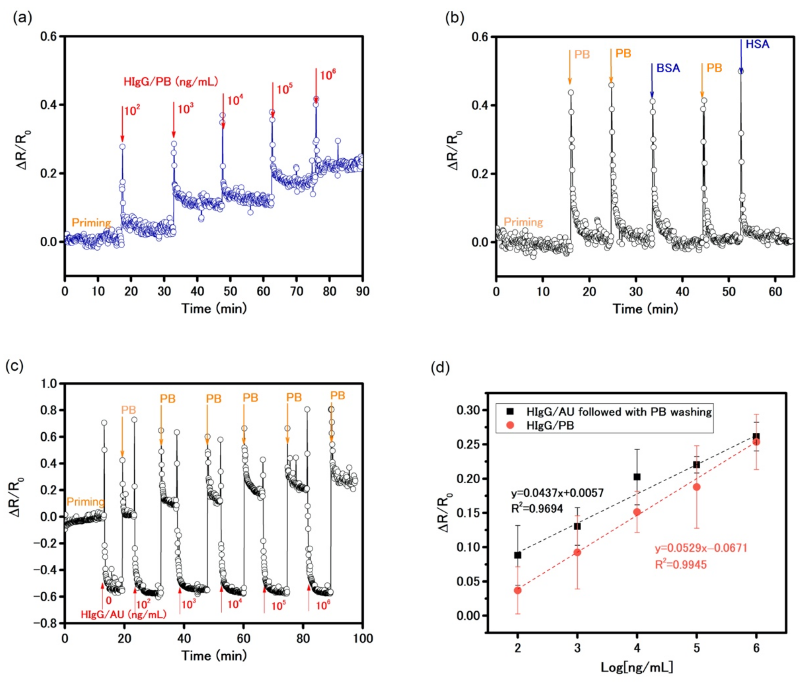
3 layers after ammonium hydroxide treatment, anti-HIgG was covalently functionalized on the device via surface chemical reactions using APTES and glutaraldehyde to construct a biosensor to detect HIgG in PB solution. The device was initially primed with PB solution for stabilization. Then, increasing concentrations of HIgG solution were injected into the cell while the resistance of the sensor was monitored for 15 min. The result in
Figure 6a shows the time-dependent change in resistance. It was evident that a spike in the readings was due to the physical injection at each injection point and yet the increase in the reading after stabilization was indeed due to increasing amounts of HIgG. It showed a stabilized signal was achieved in an average of 2 min after each addition of the target solution. It is important to note that the oxide layer, due to the strong n-doping effect, permitted electrical measurement without requiring a back-gate potential that allowed a more facile and low-power mode measurement. The biosensor exhibited good sensitivity by showing clear responses to HIgG solution of concentrations down to 100 ng/mL, as well as high selectivity with non-response to PB solutions, 10
5 ng/mL of BSA, and 10
5 ng/mL of HSA solutions, showed in
Figure 6b. The calibration curve plotted in
Figure 6d shows a linear relationship (y = 0.0529x − 0.0671; R
2 = 0.9945) between HIgG concentration and the percentage change in resistance within a wide dynamic range from 10
2 to 10
6 ng/mL in PB solution. The sensitivity of 0.0529 per Log
10 (ng/mL) was obtained from the slope of the response (∆R/R
0) as a function of HIgG concentration, where R
0 is the resistance of the device established with PB solution in the priming process and ∆R is a resistance change caused by affinity binding of HIgG antigen-antibody interaction. From the noise data of the PB baseline in
Figure 6a, root-mean-square value of ∆R/R
0 noise of ~0.034 was obtained. The limit of detection (LOD), defined as 3 × SD/m (where SD is the standard deviation of the blank and m is the slope of calibration plot), was estimated to be 83 ng/mL. Additionally, the small error bars demonstrate good reproducibility, which assures a reliable consistency in detecting HIgG.
A biosensor that can be used directly with physiological samples is much favored and very demanding. The sensor was further used to detect the HIgG in an artificial urine (AU) matrix (pH = 7.4), which simulated the real-life human body fluids sensing environment [
37]. Since the AU has high ionic strength due to a lot of salts, it reduced the Debye length and thereby sensor response. To alleviate this problem, we introduced the washing of the sensor with PB solution to reduce the ionic strength post antibody-antigen binding to recover the responses of MoS
2-based biosensor.
Figure 6c illustrates dynamic response of the biosensor at an applied source-drain voltage of 1 V (with no gate voltage) to 0–10
6 ng/mL HIgG in AU. After PB priming, the injection of increasing concentrations of the target in AU produced large negative responses, which were opposite to the response obtained in PB (
Figure 6a). After washing the test cell by 800 μL of PB, the responses became positive and showed agreement with the responses in PB. The calibration plot of the biosensor to HIgG in AU, shown in
Figure 6d, had a linear relationship with the sensitivity (slope) of 0.0437 per Log
10 (ng/mL), which was in very good agreement with the sensitivity of 0.0529 per Log (ng/mL) in PB. These results present a simple approach for overcoming the effects from organics and salts present in AU and a high degree of accuracy even in a complex real-life sensing environment. Comparison with recent literature results on MoS
2-based FET biosensors, presented in
Table S1, clearly indicates the comparable performance of our MoS
2 biosensor based on simple chemiresistive principle using modulation of resistance instead of FET principle based on change in transfer characteristic of the device.

 ,
, 