Abstract
Thickness dramatically affects the functionality of coatings. Accordingly, the techniques in use to determine the thickness are of utmost importance for coatings research and technology. In this review, we analyse some of the most appropriate methods for determining the thickness of metallic coatings. In doing so, we classify the techniques into two categories: (i) destructive and (ii) non-destructive. We report on the peculiarity and accuracy of each of these methods with a focus on the pros and cons. The manuscript also covers practical issues, such as the complexity of the procedure and the time required to obtain results. While the analysis focuses most on metal coatings, many methods are also applicable to films of other materials.
1. Introduction
The use of thin films has become a ubiquitous practice across much of the scientific and industrial sector. Coatings are widely used to obtain a synergistic action between the characteristics of the substrate and the covering material. They can enhance physical, chemical and aesthetic properties and lower the costs of the final product. For all these reasons, measurement of the thickness in composite materials is mandatory, both to obtain the right characteristics in the final artefact, as well as to keep the costs under control. The nature of the films may be extremely vast, and dielectrics (organic, such as polymers and self-assembled monolayers (SAM), or inorganic, such as metal oxides), semiconductors and metals are all used in the formation of films. In this study, we focused on the characterization of metallic films obtained through electrodeposition or vapor phase deposition, but most of the techniques mentioned in this article can be applied to films used for different materials. As far as the dimensions of the film are concerned, the thinnest measurable thickness coincides with an atomic monolayer (ML), while the thicker layers can reach hundreds of microns in the case of electroforming. Therefore, in this review, we carried out an overview of all the investigation techniques in this range.
According to the type, composition and thickness of the film itself and the substrate, various methodologies can be employed to investigate the thickness of the layers [1]. The processes can be classified into two different categories: destructive and non-destructive techniques.
A destructive technique permits the direct measurement of the thickness. This requires the sample to be modified at the macroscopic or microscopic level; therefore, the analyzed sample cannot be used and must be disposed of. On the other hand, a non-destructive technique facilitates the measurement of the sample without damaging it. Indirect measurements fall into the category of non-destructive techniques, in which some assumptions and calculations have to be performed to obtain a numerical value of the thickness. Many destructive methods require a specific sample preparation step, while non-destructive methods are usually self-consistent and require minimal—if any—preparation of the sample.
The preparation methods covered in this review include cross-sectioning, transmission electron microscope (TEM) lamella preparation, angle lapping and the Calo test. Cross-sectioning and the Calo test are macroscopic methods, while TEM lamella preparation and angle lapping are microscopic procedures performed mechanically or with a focused ion beam. In any case, all of them are destructive and are needed before any microscopic analysis, whether it exploits light, such as optical microscopy; electrons, in the case of scanning electron microscopy (with both backscattered (BSE) and secondary (SE) electrons), transmission electron microscopy and scanning transmission electron microscopy (STEM); or ions, e.g., scanning ion microscopy (SIM).
Another destructive preparation method involves masking the sample to leave the substrate partially uncovered to analyze the height profile with a profilometric technique [2,3].
Additional analytical techniques only require the sample surface to be properly cleaned. These techniques analyze the sample along the direction perpendicular to the surface instead of using a lateral view of the cross-section. Regarding the microscopy techniques, these do not provide direct information about the thickness and the signal must be analyzed to deconvolute all the information that it contains. For this reason, we must obtain as much information as possible about the sample to make the right assumptions based on its nature and to obtain reliable results. In addition to being an excellent technique for compositional determination, X-ray fluorescence spectroscopy is by far the most common technique used in the industrial field for thickness measurement and quality control, as it allows for fast, non-destructive analysis with minimal sample preparation [4]. XRF is a very versatile technique, since the sample can be either solid or liquid, a metal or a dielectric. Most of the elements can be detected in normal ambient conditions. For the lighter elements the measurements are performed under vacuum conditions or a helium atmosphere, because most of their emission is absorbed by air. The thickness can be extrapolated from XRF data by means of standards [5], using the analytical equations of the fundamental parameter method (FP) [6] or through Monte Carlo (MC) simulations [7,8,9]. Other non-destructive techniques, more commonly used for research purposes, include ellipsometry [10]—however, this is rarely applicable to metallic coatings (it is mainly adopted for optically transparent coatings)—and X-ray reflectivity (XRR) [11,12] that can detect thicknesses that range from tens of nanometers to a few micrometers. Although they are commonly used for quantification purposes, even electron probe microanalysis (EPMA) [13,14] and X-ray photoemission spectroscopy (XPS) [15,16,17] can be employed to determine thickness information up to the atomic scale. The methods used for deconvolution of the signal range from the use of standards [13,18], MC simulations [19,20,21], attenuation length [22,23] and three-layer-model or multilayer model analysis [24,25,26,27,28,29]. Additionally, Rutherford backscattering spectroscopy can be used for the determination of film thickness [30,31]. Furthermore, the thickness of a coating can be determined by destructive sputtering techniques [32] in which the sample is bombarded with ions, the surface is slowly removed, and the emitted elements are analyzed by carrying out a depth profiling analysis. Depth profiling analysis can be performed with secondary ion mass spectrometry (SIMS) [33,34] or XPS sputtering. Data interpretation and thickness evaluation can be performed using the Laplace transform or maximum entropy method [35,36,37,38,39]. All of the techniques covered in this review are summarized in Table 1.

Table 1.
Summary of the techniques covered in the review.
2. Destructive Techniques
2.1. Preparation Methods
2.1.1. Mechanical Cross-Sectioning
The cross-section technique is ubiquitous and relatively simple to use, even if it requires particular attention and manual skill of the operator [40]; in fact, if not executed carefully, it can lead to inaccurate measurements. Cross-sectioning is an ISO- and ASTM-standardized procedure [41,42,43]. It consists of cutting the sample in half and observing it transversely along the profile of the layers of which the thickness must be measured. This technique, therefore, allows for direct measurement of the thickness of the film using a ruler. The entire analysis process consists of three steps: sample preparation (cutting, embedding and lapping); microscopic analysis through optical or electronic microscopy; and data processing through dedicated software to convert the image dimensions from pixels into a unit of length through a scale.
The sample preparation process is the most critical and time-consuming step; it is during this stage that artefacts that can invalidate the subsequent analysis can be generated. Usually, the sample is sawn using a disc cutting machine with the use of an abrasive resin disc or a diamond disc, but, if feasible based on the characteristics of the sample, it can also be cut in other ways such as with a cutter or scissors. The cut must be made perpendicular to the surface, otherwise the thickness analyzed will be overestimated due to parallax error. Moreover, the cut must neither be too fast nor overheat the sample in order to avoid damaging or detaching the film; for this reason, many saws are equipped with a liquid cooling system with a direct jet on the sample.
If our goal is to accurately measure the thickness of the outermost film, which is very thin, the cut can compromise the analysis. To avoid this problem, if the sample is conductive, it can be covered with a galvanic deposition of a few microns in order to protect the layer of interest. Alternatively, the sample can first be incorporated in resin and then cut later; however, in this case it is more difficult to perform a cut perpendicular to the surface. Moreover, the hardened resin tends to shrink, not remaining perfectly adhered to the sample and reducing the protection of the external film.
The incorporation can be performed with both hot melt and cold resins. The sample is placed in a housing, ensuring that it is perfectly level, and the resin is poured, being careful not to leave air bubbles. The resin used can be either conductive or non-conductive. If the sample is to be analyzed under an optical microscope, conductivity is not a factor; therefore, non-conductive resins are preferred because they are cheaper. On the other hand, if analysis is to be carried out through electronic microscopic analysis, a conductive resin is preferable to avoid polarization phenomena, although a non-conductive resin can also be used if it is possible to graphitize the sample.
The last step in sample preparation is lapping. Near the cut, the sample will inevitably be damaged, and the films will be altered; there may be peeling of the films, meaning the detachment of the less adhered films, and a spreading of the softer films. The lapping process is the longest phase; it can take several hours and consists of polishing the section of the sample with gradually finer abrasives until a mirror surface is obtained. The surface roughness and scratches must be minimized in order to accurately measure the thicknesses; as a rule of the thumb, the surface roughness and consequently the abrasive grain size must be in the same order of magnitude or less of the thickness to be analyzed, generally 0.3–1 micron. The lapping process can be carried out by hand or using special automatic lapping machines. Wet abrasion is carried out first using gradually finer sandpaper and then with a cloth soaked in an abrasive suspension. The suspended particles can be alumina or diamond dust. Initially, with sufficiently coarse sandpaper, the entire part that was damaged during cutting is removed, about 1 mm in depth; then, the grain size of the sandpaper is decreased. Fine-grain size is not used immediately, as it would not be possible to remove the deepest scratches. In the event of lapping by hand, the sample must not be pressed too hard, and care must be taken not to consume one side more than the other to avoid introducing a parallax error. For this reason, it is advisable to rotate the sample in the same direction as the lapping machine disk and occasionally turning it by 90° with respect to its normal axis. When the sample is thought to be ready, it is washed and inspected visually or, if available, under an optical microscope to check that all the scratches have been flattened. If the sample is sufficiently smooth, the next phase of microscopic analysis can be carried out. By way of example, a microscopic analysis of the same cross-section is shown in Figure 1, where a comparison between an optical and electron microscope is shown in the image. The multilayer sample is made of brass/Cu/bronze/Pd/Au/Ni. With the optical microscope, it is possible to distinguish most of the layers. Even the thin gold layer is visible, although not quantifiable; it is not possible to discriminate between the bronze and palladium layers. Layers with a thickness over 500 nm can be measured with an optical microscope, but for thinner coatings, and to distinguish brass and palladium, the electron microscopic image is necessary.
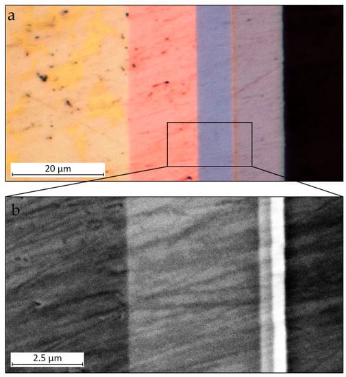
Figure 1.
Cross-section multilayer sample (brass/Cu/bronze/Pd/Au/Ni) observed with an optical microscope (a) and electron microscope (b).
2.1.2. Focused Ion Beam Cross-Sectioning
Another series of techniques enabling fast characterization of thin metallic films employ focused beams of ions. Ionic probes display different beam–matter interactions concerning electrons, resulting in other effects of the impinging beam on the surface [44,45,46,47,48,49]. First of all, it is worth noting that the ion beam–matter interaction always modifies the surface of the sample (often in a destructive way, which must be taken into account for each one of the ion methods listed below). Particularly, when an ion beam hits a surface, it can generate a series of different effects with respect to an electron beam; all these effects are a consequence of elastic or inelastic collisions between the charged particles and the atoms forming the surface. The most important interactions can be listed as follows: (a) surface sputtering, (b) secondary ion emission, (c) deformation of the surface reticule, (d) ion implantation, (e) emission of electrons, (f) emission of electromagnetic waves and (g) heating. All these effects manifest at the same time; their ratio is strongly dependent on the physicochemical nature of both the probe and the targeted surface, and on the apparatus set-up. For a specific ion source, parameters such beam energy, beam current, and impact angle can be tailored to favor one phenomenon with respect to the others; as an example, by decreasing the accelerating voltage of the emitted ions, it is possible to decrease the deformation of the surface lattice (amorphization) strongly at the cost of reduced control over the ion beam. Among all the ion beam–matter interactions, three are used for the characterization of thin metallic films: (a) the production of electrons [50], (b) the sputtering of neutral surface atoms [51] and (c) secondary ion (SI) emissions [52]. The first one exploits a signal that is similar to the one used for SEM imaging, which permits the acquisition of topographic information of the surfaces. The second phenomenon allows subtractive manufacturing to be performed on the sample surface, exposing details of its inmost structure. The third enables qualitative and quantitative analysis of the nature of the material. An FIB apparatus can permit both thin film preparation and analysis in a single workflow by preparing the surface cross-section and acquiring its images, though not all FIB columns are fitted to perform both processes well. As already mentioned, different elements can be used to produce ions; their charge/mass ratio can modify the sputtering ratios, manifesting profoundly the production of SI and SE. Today, the main commercial FIB machines are engineered to work using He, Ga, Ar or Xe ions [53]. Smaller ions, like He, are well suited for imaging purposes, while larger ions like Ar and Xe are used for fast sputtering; Ga FIB machines are considered a good trade-off between the two effects and are still considered to be the best choice for all purpose tasks.
From a technical point of view, FIB machines are very similar to SEMs. Both of them have a column that can be divided into (a) a top part composed of the source, responsible for the ion/electron generation and (b) a bottom part, the focusing apparatus, a series of electrostatic/electromagnetic lenses, condensers and apertures to focalize and control the beam [45]. In FIBs, the working principle exploited for ion emission varies depending on the physicochemical properties of the element of choice; we can divide the sources into three main branches: gaseous field ionization sources (GFISs) for He [54], liquid metal ion sources (LMISs) for Ga [45] and plasma sources for Ar and Xe [55,56]. Despite SEMs, in FIBs, the focusing apparatus is composed of electrostatic rather than electromagnetic elements (lenses, condensers, etc.). Ions in fact suffer weakly from Lorentz forces due to their slower travelling speed (with respect to electrons) in the column, also meaning that these instruments are less prone to suffer from stray external magnetic fields. Ion sources are not interchangeable; the focusing apparatus has to be finely engineered to suit the particular physical properties of the emitted element. This means also that the choice between different FIB machines, exploiting different sources, has to be carefully planned with respect of the need. Historically, industrial FIB columns were intended as standalone instruments; these devices were used especially in the semiconductor/electronics industry, where their use both for quality checking and prototyping decreased from the 1970s. Today, FIBs can be found mainly when paired with an SEM column [57]. This double column configuration allows for a vast array of different procedures for the characterization of materials in a range from mm down to the nm for all R&D fields. Moreover, FIB/SEMs can be equipped with a vast array of accessories and sensors to enable different characterization techniques, fully exploiting both the electron and the ionic beam. Particularly, all the FIB methods are well suited to the characterization of metallic films of thicknesses ranging from 50 µm down to fractions of a nm.
Among the available accessories, the gas injection system (GIS) has particular relevance, as it allows for additive manufacturing in the range of tens of nm using both ionic and electronic beams [58,59,60]. The GIS is constituted by a series of external reservoirs containing the precursors of the elements to be deposited onto surfaces, which are heated to produce a reactive gas. A hollow needle injects this gas in the vicinity of the surface of the sample surface. The beam–molecule interaction results in the degradation of the precursors followed by precipitation of the precursor elements onto the surface. Various elements can be deposited in this way; among them, the most common deposits are constituted by W, Pt, Au, Cr and C [59,60,61].
A cross-sectioning procedure can also be performed by focused ion beams. By exploiting the sputtering effect of FIBs, it is possible to raster a surface producing precise trenches, which can be used to observe the in-depth evolution of the sample [62]. The trench dimensions can vary from mm (for Xe or Ar plasma FIBs) to less than 1 µm, with a maximum depth in the range of hundreds of microns. Due to the small dimensions of the holes produced on the surface, this process (unlike mechanical cross-sectioning) is sometimes considered to be semi-destructive. FIB cross-sectioning is also faster with respect to mechanical cross-sectioning, because it permits one to produce clear cuts in 20–60 min (depending on the size of the hole) without the need for further polishing. For these reasons, it is particularly well suited for the characterization of thin films having thicknesses smaller than microns. Due to the small dimensions of the cross-sections, SEM, SIM or EDS analysis are usually adopted as subsequent characterization techniques.
Even if the cross-sectioning process can be performed only by using an FIB for the coarse determination of thick films, precise determination of films down to 10 µm will require the use of an FIB/SEM equipped with the GIS. This is because in order to avoid FIB-induced surface erosion, the surface of interest has to be covered by a thin protective layer. In FIB/SEMs, the protective layer is produced by a two-step deposition process. First, a thin layer of metal is deposited on the surface using the electron beam (e-beam deposition). Then, a thicker metallic layer is deposited using the ionic beam (i-beam deposition). The e-beam deposition is needed to avoid surface degradation (and thus loss of thickness information on the topmost layer) due to direct impingement of the ionic beam on the surface [63]. The full workflow for the preparation of a cross-section using an FIB is shown in Figure 2.
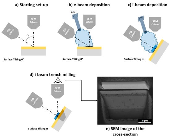
Figure 2.
An example of FIB cross-sectioning workflow: (a) the sample is inserted in the chamber with 0° tilt; (b) a thin layer of metal is deposited on the surface using the electron beam; (c) the stage is tilted and a thicker metallic layer is deposited using the ionic beam; (d) the focused ionic beam is rastered on the surface creating the cross section by sputtering effect; (e) final SEM image of the cross-section.
2.1.3. Angle Lapping
Angle lapping is a sample preparation method used to increase the resolution in thin-film thickness determination of the adopted microscopy characterization technique; it is based on a change in cutting geometry for cross-sectioning.
During traditional preparation procedures, to obtain the stratigraphic information from the sample, the cutting plane is perpendicular to the surface (θcut = 90°) [64]. The uncovered section gives direct stratigraphic data on the displacement and thicknesses of the layers above the substrate. However, in angle lapping, the sectioning cut is performed at very low angles with respect to the sample surface (θcut < 10°) (Figure 3). This produces a “magnification effect” on the newly created section surface, on which all the layers appear stretched. Knowing the cutting angle and using trigonometry, it is consequently easy to derive the film thickness. The main advantage of this method is the magnification effect, which allows the resolution limits of the microscopic technique adopted for the quantification to be overcome, even for extremely thin films. A very flat film surface is mandatory for the precise determination of the thickness of the layers underneath; moreover, the operator must put special care into the preparation of the surface after the cut. It is common, especially for mechanically-machined soft materials, to introduce thin-film deformation onto the cutting surface [65]. The origin of this sample preparation technique comes from the first metallographic studies, and it is still considered as a valuable and low-cost method to overcome the resolution limits of optic microscopy characterization methods. In time, its adoption has shifted to FIB cross-sectioning or lamella preparation, enabling fine characterization of ultrathin films.
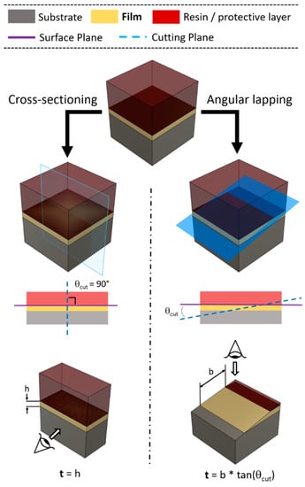
Figure 3.
Comparison between film thickness determination: traditional cross-sectioning (using a cut perpendicular to the surface, (left column)), and angle lapping (using small cutting angles in respect to the surface, (right column)).
2.1.4. TEM Lamella Preparation
The ultimate procedure for thickness determination of thin films is the TEM lamella preparation process. During this preparation procedure, a small portion of the sample surface, usually a 10 × 5 × 1 micron solid, is extracted from the sample surface. This parallelepiped shaped lamella is then thinned down to less than 100 nm to be observed transversally, to uncover the surface stratigraphy [66,67]. The TEM lamella preparation process is relevant to characterize thin films (below 1 µm) using electron beam methods. The small thickness of the lamella decreases the interaction volume abruptly, cutting down the signal coming from in-depth SE and BSE during SEM (sharpening of the image), and permitting electron transmission during TEM or STEM (Figure 4).
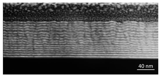
Figure 4.
STEM dark-field image of a lamella with Pd/CeO2 multilayer (each layer is less than 5 nm thick). The lamella was prepared by FIB/SEM methods.
To prepare a lamella, an FIB/SEM equipped with a GIS and a nano manipulator is required. Moreover, the lamella preparation process is quite complex and is constituted by numerous steps that can vary depending on the load-out of the adopted machine, on the geometry of the sample chamber and on the sample architecture. Generally, the workflow can be divided into three main stages: In the first step, the lamella is shaped (carved) directly onto the surface of the sample. In the second step, called lift-out, the lamella is detached from the sample and is mounted on a TEM support grid. In the third step, the lamella is finally thinned down to enable transmission electron analysis. This last process is the most delicate for the obtainment of clean, defect-free lamellas. In Figure 5, an example of a workflow for a Tescan GAIA 3 FIB/SEM is shown.
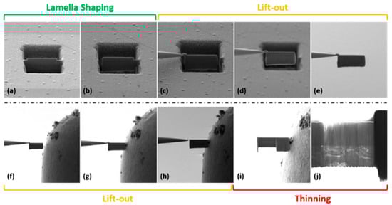
Figure 5.
SEM images of the main steps regarding TEM lamella preparation. (a) A raw lamella (about 10 × 5 × 1 microns) is carved on the surface; (b) an undercut is performed in order to detach the lamella; (c) a nanomanipulator is moved on the side of the lamella and soldered to the body, and then the lamella is detached from the surface; (d–f) the lamella is moved from the surface of the sample to the TEM support; (g) the lamella is soldered to the support; (h) the nanomanipulator is detached from the lamella; (i) the lamella is thinned down until electron-transparency; (j) in the end, lamella quality is tested using the microscope in-built STEM detector.
The lamella preparation procedure enables the study of coatings even at sub-nanometric lateral resolution (for HR-TEMs).
2.1.5. Calo Tester
The Calo tester, also known as a ball crater or crater grinding, is a semi-destructive technique that is not very widespread but extremely practical in some cases; in addition, it is regulated in ISO 26423 [68] (Ex EN-1071 and VDI 3198 [69]). Compared to the cross-section, it has the advantage of being only locally destructive; therefore, the sample, instead of having to be cut in half, is excavated in an area with a diameter of about one millimeter [70,71]. Furthermore, the analysis is much faster, as the sample does not have to be incorporated and lapped.
This technique consists of fixing the sample on a variable angle support, onto which is placed a steel sphere covered by an abrasive suspension; the sphere is also in contact with a rotating cylinder that makes it roll (Figure 6). Within a few minutes, depending on the hardness of the sample and its angle of inclination, which is translated to the weight that the sphere impresses on it, a circular crater will form, revealing all the layers [72]. Since the abrasion angle is small (due to the diameter of the sphere), layers of even a few microns will have a much greater apparent size and can be appreciable under a standard optical microscope. As in the case of the cross-section, only the layers having a different color can be distinguished. Once the diameters of the concentric circles that have been created on the sample have been measured, using a dedicated formula (Figure 6) that takes into account the diameter of the abrasion sphere, the real thickness of the films can be obtained. Manufacturers ensure that the range of thicknesses that can be measured is between 50 and 0.1 microns.
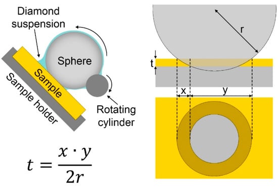
Figure 6.
Experimental setup, working functionality and equation to calculate the film thickness (t) with a Calo tester; r is the radius of the sphere; x is the difference between the radius of the crater and radius of the part of the crater at the bottom of the coating; y is diameter of the crater from which it is subtracted x.
2.2. Microscopic Analysis
2.2.1. Optical Microscopy
To measure a cross-section of a sample, it is necessary to use the microscope in reflection mode; additionally, to be able to recognize the different layers, it is essential to have sufficiently high contrast, or more simply, different colors. Distinguishing different layers made, for example, of the same silvery metals, is impossible, while it is straightforward to measure, for example, a silver film on copper or brass.
The lateral resolution, i.e., the minimum distance between two resolved points, is defined by the Abbe principle. The resolution is related to the wavelength of the source used, in this case, the visible photons. The theoretical resolution of an optical microscope, not taking into account optical aberrations, using white light is about 0.2 microns. However, more realistically, the measurement of film with a thickness of less than one micron is difficult and has a consistent uncertainty [73,74,75,76].
2.2.2. Electron Microscopy
Scanning electron microscopy is used when the thicknesses are too small to be analyzed with the optical microscope, or if the layers have an optical contrast among them that is too low. As a general rule, if the cross-section of a sample can be adequately analyzed with an optical microscope, there are no valid reasons to use an electron microscope; in fact, the sample needs some characteristics in order to be measured with an SEM. Moreover, SEM analysis is intrinsically more expensive than a simple optical analysis. Despite this, for most coatings, optical microscopy is not enough to obtain adequate results. A sample that is analyzed by SEM must be stable in high vacuum (about 10−7 bar), under irradiation by an electron beam and must be conductive. These limitations can be circumvented by means of certain techniques: there are specific environmental or low-vacuum SEMs that allow analysis to be carried out with a pressure in the order of one Pascal; the acceleration potential of the electron beam can be reduced to a few kV in order not to damage the sample (but with a consequent decrease in image quality); non-conductive samples can be graphitized to avoid the accumulation of surface charges that, in this way, are dispersed to ground. However, these problems arise when biological, organic or polymeric samples are analyzed; for metallographic cross-sections, there are rarely complications of this type.
Numerous advances have been made in the last few decades in the field of electron microscopy. The resolution of these instruments is quite variable and ranges from about 20 nm for older instruments with thermionic emission, up to less than the nanometer scale for new instruments with a field emission source (FEG-SEM). In SEM, the main limit to the resolution is not so much the wavelength of the probe, the electrons, as it is the diameter of the beam and therefore its focus and collimation. For this reason, a stratagem to improve the resolution consists in bringing the sample closer to the source, reducing the working distance and, consequently, the opening of the electronic beam cone. The SEM images can be acquired using secondary electrons, backscattered electrons or through a microanalysis map. Because of the different nature of the signals, they differ in the depth from which the signal comes (Table 2) and in their volume of interaction (Figure 7). A higher volume of interaction results in a lower lateral resolution, which translates into a less clear separation of the edges between the films that have to be analyzed [1,14].
Table 2.
Penetration depth of SE, BSE and EDS in Al and Au with a 20 kV beam.
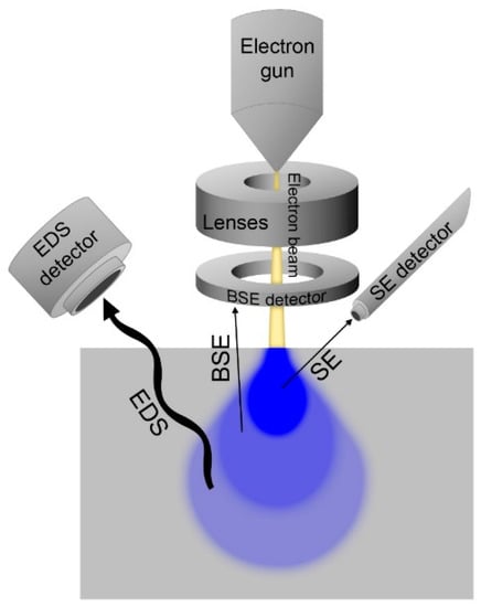
Figure 7.
Scheme of a SEM with SE, BSE and EDS volume of interaction and detectors.
SEs are produced when a primary electron from the beam excites an electron of the atoms of the sample to the point of tearing it from the nucleus; these electrons are low in energy (<50 eV), and only those generated most superficially on the surface are detected (Figure 8a). SEs carry the morphological information with them, so the contrast in the image is based on the heights of the sample. Since our sample has been levelled, the contrast produced can only be due to the different natures of the material. The SE in small part also contains information on the composition, since the number of electrons emitted is proportional to the atomic number of the element under the electron beam. Thus, layers of elements with significantly different atomic numbers can be distinguished [77,78]. A trick that allows similar elements to be observed with the SE is to chemically etch the sample before the analysis in order to slightly corrode one material compared to another; in this way, morphological differences, clearly visible to the SE, are reintroduced between the different layers. However, the etching must be studied appropriately with respect to the sample that has to be analyzed.
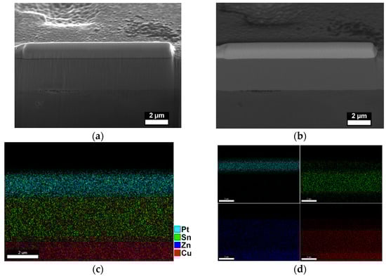
Figure 8.
Example of a multilayer sample (Pt/bronze/brass) analyzed with (a) secondary electrons; (b) backscattered electrons; (c) energy dispersive X-ray spectroscopy convoluted map; (d) single elements EDS map.
BSEs are the primary electrons which, interacting with the positive nuclei of the atoms of the sample, are backscattered towards the source; for this reason, they are very energetic and penetrating (Figure 8b). Therefore, BSEs carry mainly compositional information; heavier elements generate more BSE. By sacrificing part of the lateral resolution, the image obtained will be much more contrasted by highlighting differences between the layers that can be below an atomic number unit for more modern systems, allowing in some cases even deposits of a metal to be distinguished from its alloy (for example, copper on brass).
Finally, the EPMA signal can be used (Figure 7d and Figure 8c). This is the signal with the highest volume of interaction, and for this reason, the lateral resolution is inferior compared to the previous ones. In this case, the objects to be analyzed are not the electrons but the X photons that are emitted from the sample after the interaction with the primary electrons, which contain detailed information on the composition. With EPMA, alloys can be distinguished, which vary in composition by a few percentage points. Then, the different layers can be highlighted by making a map or a linear scan perpendicular to the layers. However, given the low lateral resolution, films just below the micron are challenging to quantify.
Another trick to increase lateral resolution is to reduce the volume of interaction, and this is possible by decreasing the energy of the electrons by lowering their acceleration potential. This dramatically reduces the signal, but with modern instruments, it is possible to obtain good images using acceleration potentials of only a few kV. This strategy is minimal; however, in the case of the EPMA, to have a good emission of the X photons, the electron beam must have indicatively an acceleration potential one and a half times the energy of the emission peak of interest.
2.2.3. Scanning Ion Microscopy
Scanning Ion Microscopy exploits electron emission from a surface when targeted with an energetic ion beam. These emitted electrons, with comparable energies with respect to secondary electrons produced in SEM beam–sample interaction, can be collected by a detector to form an image. Like scanning electron microscopy, SIM can be used for the study of cross-sections, bringing more surface-sensitive images. Ions tend to have smaller mean free paths inside the matter with respect to electrons [54,79]; this smaller beam–surface interaction volume brings crispier, less bulk-mediated images. Moreover, the number of SEs produced per impacting ion is larger compared to the number of SEs produced by the impact of an electron, which leads to an enhanced signal [80] even at low ionic currents. In the end, due to their dimensions, ions tend to be particularly sensitive to crystal orientation; images acquired by SIM possess stronger crystalline contrast, due to the channeling effect [81], with respect to their SEM counterparts. Despite all these strong points, two technical downsides prevent SIM from being a valuable alternative to SEM. Ion image acquisition is a destructive process; beam rastering alters the surface of the sample by producing sputtering. Furthermore, even with recent beam-columns, SEM resolutions still cannot be reached. The most common LMIS sources are able today to obtain a resolution of tens of nanometers (about 20 nm for Ga), strongly depending on the chemical nature of the primary ions.
SIM microscopy can usually be performed in every FIB/SEM apparatus, using every ion source, and by adopting the Everhart–Thornley scintillator used for SEM SE imaging [14]. This detector can also be found in standalone FIB machines, which are more difficult to find today due to the wider diffusion of combined FIB/SEMs. Only a particular dedicated SIM device still holds a small portion of the market, namely the helium ion microscope (HIM). This microscope represents one of the best machines for ultimate scanning imaging. HIM is in fact capable of delivering very narrow beam spots, bringing resolutions below 0.27 nm with minimal bulk interaction volume [80,82,83]. Moreover, due to its chemical nature, the use of He minimizes implantation and reaction phenomena that can occur when adopting more reactive ions like gallium.
2.2.4. Data Analysis
Once the image is obtained with a microscopic technique, pixels must be converted into a unit of length. Most the software that allows microscopic images (both optical and electronic) to be acquired commonly have a tool for the extraction of this information; otherwise, there are free or paid for software that allows the same job to be done, e.g., ImageJ, Gimp and Adobe Photoshop. In order to convert the pixels to lengths on the image, a reference scale must be printed on it, and through that scale, all the dimensions of interest in the image can be obtained. The thickness of the films can therefore be measured, with the appropriate care taken to ensure the measurement is perpendicular to the film. By making the measurement at several points, statistics of the thicknesses can also be carried out. However, in the event that the edges of the film in the image are not very defined, finding the limits by eye can be difficult, as shown in the blurred image of an Au film reported in Figure 1. In these cases, instead of analyzing the image, it is more practical to observe the profile graph in which the greyscale values are reported. If the different layers have a contrast between them, they also have a distinct grey value; the delimitation between one layer and another can be defined as the point where the value is intermediate between the two layers or, more rigorously, at the inflexion points of the graph. In this case the spatial resolution, and therefore the uncertainty of the measurement, is defined as the distance between the points where the variation of the grey value is in the range of 20%–80% [84], as required by ISO 18516 [85]. On the other hand, an incorrect method to make the separation of the layers more defined is to digitally postprocess the images by acting on brightness and contrast. In fact, as opposed to varying these parameters during the measurement, by performing software alterations of the image, the edge of the film can move as the different shades of grey are processed, as demonstrated in Figure 9.
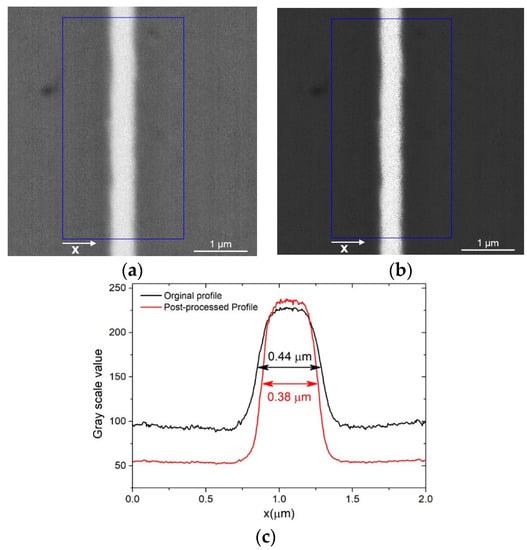
Figure 9.
(a) Au film between two Cu layers, the image shown as acquired from the instrument; (b) the same image as (a) but post-processed to enhance the separation between the layers; (c) plot profile of the images (a,b) and the extrapolated thickness of the Au film.
2.3. Profilometry and Scanning Probe Microscopy
Profilometry is a class of techniques that permits the characterization of the line profiles of surfaces. It can be divided into non-contact and contact profilometry, depending on the probe used. In non-contact profilometry, light is used as the probing medium; information is then extracted using interferometric methods. On the contrary, contact profilometry relies on the use of a sharp needle, the tip of which is shifted horizontally on the sample surface by following a predetermined pattern. During this in-plane (x–y) movement, the needle is free to move on the vertical (z) axis according to the surface profile, and thus to collect the height value with respect to the horizontal movement, giving a line-profile of the surface [86]. Contact profilometry is the oldest profilometric technique but is still widely adopted in industrial contexts to acquire fast information on surface roughness. Contact profilometry can also be used to determine the thickness of thin films adopting the “scratch method”. This technique exploits discontinuities on the coating surface, which uncover the base substrate underneath. By horizontally moving the tip between the substrate surface and the coating surface, it is then possible to record a height difference between the base material and film surface and thus determine the value of the coating thickness (Figure 10). Despite its apparent simplicity, the scratch method has some intrinsic limitations: (a) Test samples have to be prepared accordingly, with coating-free zones for the substrate height measurement or (b) a scratch has to be performed on the continuum of the sample coating, to uncover the substrate. This second procedure is risky because the base surface can easily be deformed by the scratching process, hindering precise thickness measurement. Moreover, coatings could show different thickness values near the boundaries with the uncovered zones, both due to a “border effect” arising during the film deposition or to plastic deformation during the scratching of the surface. It is then mandatory to perform various line acquisitions to acquire some profile statistics.
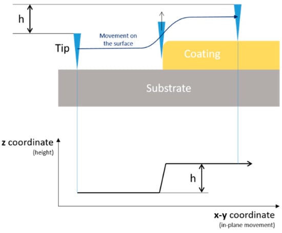
Figure 10.
Line-scan performed using the “scratch method”, side-view; h represents the measured height.
Scanning probe microscopy (SPM) can be used to perform thickness measurements. This class of techniques, which is considered as a subgenre of contact profilometry, exploits different tip–surface interactions to trace the surface profile; mechanical contact, van der Waals forces, capillary forces, electrostatic forces and chemical bonding are among the most important ones. Atomic force microscopy (AFM) [87,88], which usually exploits mechanical interactions between the probe and the surface, can be considered as a natural evolution of contact profilometry. AFM permits a surface to be reconstructed by acquiring parallel line profiles, which can be stitched to form an image that contains 3D information of the surface. Just like contact profilometry, AFM uses a small needle mounted on a cantilever to acquire the surface image. The rastering of this probe across the surface is responsible for the acquisition of line profiles, which are encoded by a laser/CCD system. AFM can work both in contact mode or tapping mode. In contact mode, the tip is shifted continuously on the surface just like in profilometric measurements; tapping mode exploits a periodic vibration of the tip on the surface [89]. The choice between these two scanning modes depends mainly on the hardness of the surface under study. The tapping mode is suitable for soft materials, like polymer films, where the continuous shifting of the tip on the surface would produce deformation and artefacts.
In contrast, for hard surfaces (most of the metallic, ceramic or semiconductor coatings/layers), contact mode can be used without producing deformation of the surface. There are also other SMP methods to acquire direct thickness of thin films. Conductive AFM (C-AFM) can be used to measure coating thicknesses in materials with high electric resistance by applying Ohm’s second law. Thickness sensitivity of C-AFM can span from hundreds of microns (for the cheaper bench apparatus) to tens of nanometers, with a scanning length that can reach tens of millimeters. AFM is much more sensitive; it can reach sub-nanometric z sensitivity, but in contrast to common profilometry has a limit in terms of a relatively small working area, which with difficultly can be at most a 50 × 50 µm2
2.4. Secondary Ion Mass Spectrometry
Secondary ion mass spectrometry exploits the ion emissions [90] that are produced from a surface when targeted by a primary ion beam to acquire compositional depth-profiles of a sample. The ions produced by the primary beam, called secondary ions (SIs), are a small percentage with respect to neutral sputtered atoms (around 1% ions, depending from the ion source and surface [91]), but they can be collected by a mass analyzer in order to acquire the elemental composition of the sample. By exploiting the destructive ion–matter interaction, it is then possible to peel layers of the surface by rastering (in a similar fashion with respect to EDS mapping) to collect the punctual SI signal and to reconstruct 3D compositional maps of the topmost layers of a surface. In order to perform SIMS, two components are needed: (1) a scanning ion column, to produce a controlled ion beam, and (2) a mass selector/detector. Again, the nature, dimension and energy of the used ionic beam deeply influences the operation parameters, in particular the SI yield. In SIMS, the same LMIS and GFIS sources can be used, with the addition of low energy clustered ions sources [92], which are more “soft” on the impact on the surface, producing larger SIs and smaller in-depth etchings [93]. Due to their low fragmentation capability, cluster ion sources are usually adopted for the study of light elements and organic molecules, such as polymers.
By contrast, the use of single ions as beam components (such as Ga LMIS) is particularly suited for elemental analysis in inorganic chemistry, due to their extensive fragmentation capability upon impacting on the surface. As regards the mass devices responsible for the analysis, they can be divided into three categories, depending on the principle used to select and separate the incoming ions: magnetic sector, quadrupole and time of flight (TOF). Time of flight is the most common for inorganic characterization [91,93,94]; it is capable of separating SIs with small charge/mass variations, usually occurring from the sputtering of hard metallic coatings, semiconductors or ceramics by means of a hard, energetic ionic beam (like Ga). TOF SIMS can be easily implemented in almost all FIB/SEM devices using the in-built ion sources.
2.5. Thickness Determination by Chemical Dissolution
To determine the thickness of a film, it is also possible to exploit the techniques of chemical analysis such as atomic absorption spectroscopy (AAS) [95,96] or inductively coupled plasma mass spectrometry (ICP-MS) [97]. The procedure consists of dissolving the film in solution and then analyzing its concentration. Knowing the surface area and the density of the material, it is possible to find the thickness of the film. Thanks to the high sensitivity of these analytical techniques, even the thicknesses of ultra-thin films can be measured. AAS is the least sensitive of the two methods, but yet it is capable of probing concentration down to 0.1 ppm. A 0.1 ppm solution obtained from an object with a 1 cm2 surface on which a material with a density of 10 g/cm3 is deposited and then dissolved in 10 mL of solution corresponds to a thickness of just 1 nm. On the other hand, if the film is very thick, the solution will be too concentrated for the direct spectroscopic analysis and a dilution will be needed.
Depending on the type of material to be dissolved, the appropriate solution must be used. The dissolution can be electrolytical [98] or chemical; in the first case, an anodic current is applied to favor the oxidation of the metal, while in the second, an oxidizing species is present in solution. The following are chemical dissolution solutions for select metals [99]:
- Zinc: hydrochloric acid; sulfuric acid; sodium hydroxide.
- Tin: sodium hydroxide.
- Copper or nickel: an oxidizing compound in combination with sodium cyanide or ammonia complexing agent.
- Silver: nitric acid; sulphonitric mixture.
- Platinum: aqua regia.
- Gold: copper cyanide and hydrogen peroxide; aqua regia.
The advantage of this method is the ability to analyze very thin layers with relative simplicity; however, there are problems that limit its use. In addition to being destructive, the measurement is not local but provides the average thickness with respect to the entire sample. Since the total metal content in solution is analyzed, and the thickness is obtained by knowing the density and area of the sample, the latter must be known exactly. For flat surfaces, it is easy to measure the geometric area, but objects with three-dimensional and complex geometries may require use of a 3D scanner or electrochemical measurements. Finally, using very aggressive solutions, it is very complex to limit the attack to a single layer, especially if we want to remove the film of a noble metal on a non-noble substrate. Then, if more than one layer contains the same metal, for example, a copper film on brass, determining the thickness is much more complicated. Furthermore, alloys can have a preferential attack of one metal over the other.
3. Non-Destructive Techniques
3.1. X-ray Fluorescence Spectroscopy
X-ray fluorescence spectroscopy is an analysis tool widely used for the elemental analysis and chemical analysis of materials. When materials are exposed to high-energy X-rays, ionization of their component atoms may take place, exciting them; during the relaxation process, characteristic X photons are emitted and detected for analysis. Due to incident high-energy X-rays, inner shell (K, L, M, etc.) transition phenomena occurs within 100 fs, producing characteristic fluorescence radiation. Ionization consists of the ejection of one or more electrons from the atom and may occur if the atom is exposed to radiation with an energy larger than its ionization energy. X-rays and gamma rays can be energetic enough to eject tightly held electrons from the inner orbitals of the atom. The removal of an electron in this way makes the electronic structure of the atom unstable, and electrons in higher orbitals “fall” into the lower orbital to fill the holes left behind. In falling, energy is released in the form of photons with an amount of energy equal to the difference between the two orbitals involved. Thus, materials emit radiation of the characteristic energies of the present atoms. The apparatus (Figure 11) consists of (i) an X-ray source or tube; (ii) a fixed or exchangeable collimator that determines the measurement spot; (iii) one or more filters to attenuate the characteristic lines of the tube and making the light more “white”; and (iv) a detector.
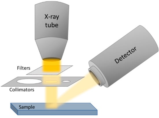
Figure 11.
Scheme of the principal components of XRF.
A variety of samples in different states, such as solids, powders and liquids, can be analyzed using this technique. It can also be used to measure the composition and thickness of coating and layers. The characteristic photons of the sample are collected by a detector that uses the same working principle of EPMA. Both the source and emitted photons can pass through an analyzing crystal that acts as a monochromator, differentiating between energy dispersive (ED) XRF without analyzing the crystal; wavelength dispersive (WD) XRF, in which the emitted photons are selected with a monochromator; and monochromatic wavelength dispersive (MWD) XRF, in which two optics are used, one for the source and one for the emitted photons. For reasons of cost and ease of use, energy dispersion instruments are the most used. The incoming high-energy beam is very penetrating (Figure 12); for this reason, the maximum detectable thickness is related to the energy of the emitted X-rays.
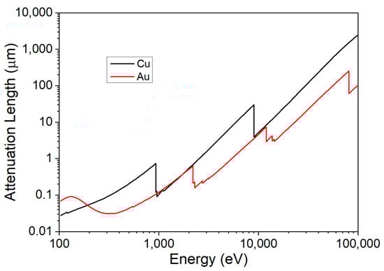
Figure 12.
X-ray attenuation length as a function of the energy of the photons for copper and gold.
XRF is the most common instrument used by industries for film thickness investigations, since it is fast, non-destructive and relatively simple to use, making it perfect for the quality control of the products [100,101]. For this reason, there are also standard procedures to measure for compliance with ISO 3497 [102] and ASTM B568 [103] regulations. Commercial instruments can measure easily the thickness of almost any material (with some restrictions for lighter elements), whether conductive or not, in the range from 10 nm to 100 µm [104,105]; nevertheless, depending on the materials under investigation and the instrumental settings, the limits of measurement can be extended from less than 1 nm [106] to a few centimeters [107]. The lateral resolution of XRF is very low, and the spot size commonly ranges from 0.1 to 15 mm. The relative intensity (normalized respect to a bulk element) of an emission from a film follows an exponential trend [19] but can be approximated to a second-order curve for small ranges far from the saturation thickness [8]. The emission of a gold film on a Cu substrate, as a function of the thickness, is reported in Figure 13 using a log–log scale. In this case, the range of thicknesses between the relative intensities of 0.9 (semi-infinite thickness [108]) and 0.1 (infinitely small) of gold is between 0.2 and 50 µm.
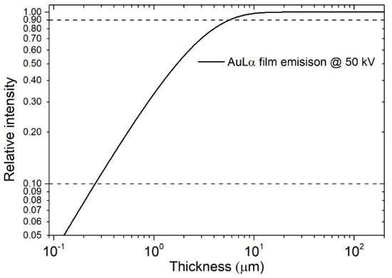
Figure 13.
Log–log plot of the emission of Au film on Cu as a function of the thickness using a 50 kV X-ray beam. The 10%–90% thickness range is marked.
The output of the instrument is a spectrum in which the position of the peaks corresponds to the spectroscopic emission of the elements present in the sample, while the intensity is correlated to the sample composition in the volume of the interaction of the incident beam. For this reason, there is no direct information on the thicknesses, but the intensity of the peaks in the spectra will be a function of thickness. A sample with a thicker coating will emit more photons from the film and fewer from the substrate than a thinner one. Since no information about the thickness can be extracted a priori from the spectra, only with the right assumptions of the nature of the sample and the use of a good calibration curve can the thickness information can be deconvoluted; this complication could bring large uncertainties or even erroneous results.
Deriving the coating’s thickness from the X-ray spectrum requires an experimental calibration curve that employs standards; however, due to the large dependence of the X-ray spectrum on the nature of the coating and the substrate, standards are not always available. The variability of thickness, layer composition, multilayer architectures and the substrate’s chemical nature creates difficulties in producing certified standards. This issue is critical in industrial applications. Indeed, the determination of precious metal coatings in the fashion industry is a major one, where the products are made with many coatings and substrates with extreme variability in the system. A calibration curve obtained with standards of known thicknesses was used to measure vanadium (V) oxide nanometric films on glass with a portable XRF measuring the attenuation of Ca emissions [5]. Hamann [109] was able to detect fractions up to 1% of a monolayer of over 20 samples without the use of standards or models, combining WD-XRF and XRD measurements to obtain the proportionality constant between X-ray emitted intensity and the number of atoms per unit area.
Nowadays, the most common approach is the use of the fundamental parameter (FP) method [6,104,110,111]. FP relies on theoretical equations that consider the composition and thickness of a sample to evaluate the XRF intensity. Practically, the FP method is combined with a few pure element empirical standards to correct unpredicted deviations due to matrix effects [112,113]. With the FP method, it is possible to determine the film thickness of single and even multilayer samples if the structure and the composition are known exactly; nevertheless, the error correlated with the measurement is significant. Typical accuracy for single-layer samples is ±5%, while for multiple-layer samples, this value grows to ±10% for the upper layer and ±37% for the first underlayer [114,115,116] due to inaccuracies in the method for complex samples.
Often, the thickness and composition of the underlying layers in multilayer architectures are not exactly known, and they are introduced in the measurement software using an initial estimation [117]. Many authors investigated the FP method for multi-layered samples in the micron range (Au/Ni/Cu [114]) as well as in the nanometer range (Ni/Cu/Si [118]). This method is advantageous when it is difficult to obtain accurate certified reference materials for layer thickness calibration, such as in the case of semiconductor research [119]. Vrilink [115] showed a good correlation between FP and SEM and profilometry measurements of multilayer samples with different compositions (Rh, Ta, W, Ti, Pd, Pt, Ni, Au, Cr) between 20 and 250 nm, considering the density variation for thin films. Ager [117] highlights the discrepancy between SEM and non-destructive techniques like RBS and XRF measurements due to differences in density between bulk metal and thin films due to porosity; in the paper, comparison between references and electroplated samples were performed to prove the hypothesis for ancient gildings, but his considerations are valid in many other fields. Exploiting the FP, both the emission line of the top layer as well as the reduction in the intensity of the underlying layer can be used for thickness determination, as shown in a study in 2017 in which the results of atomic layer deposition (ALD) oxides samples were tested [108].
An alternative to the use of standards and the FP method consists of a semiquantitative approach based on calibration curves obtained with simulation software using MC algorithms. During the simulation, when the materials and the architecture to simulate are chosen, it is also possible to specify the density of the materials; in this way, the user can decide to simulate materials that have a porosity different from the nominal one due to the deposition method, as for example happens during electroplating in which the density of the coatings is often lower than that of the bulk material. Moreover, the MC method simulates X-ray spectra using a statistical approach that counts the photon interactions in the sample. With this approach, inhomogeneities of the sample, spectral and spatial distributions of the beam, polarization effects, photo-absorption, multiple fluorescence and scattering effects, which are difficult to model with the FP method, can be considered. The simulation approach is not very common, probably because the FP was preferred for many years since it was computationally favorable, but with the latest technological development, even a personal computer can be used to obtain a good simulation in a relatively small amount of time. The two main software programs that provide a simulated spectrum with the MC approach are XRMC [120] and XMI-MSIM [121]. Both codes use the Xraylib database [122,123]. XRMC is generally used for complex 3D geometries, while XMI-MSIM can only simulate samples composed of parallel layers; however, for simple geometries, XMI-MSIM is currently superior to XRMC in simulating XRF experiments [124]. Thickness evaluation using the MC method is widely used in the field of cultural heritage applications. Schiavon [125] used XRMC code to obtain the thickness and composition of Nuragic artifacts, comparing the simulations with the experimental measurements to confirm hypotheses based on bulk chemical composition, structural observations and historical information. A similar approach was used by Brunetti [126] and Bottaini [127] for Peruvian and Portuguese artifacts; an MC simulation was performed defining the experimental setup and the sample, and then the simulated spectra were compared to the measured one visually and with the chi-squared test. If differences were found, the model was corrected until the two spectra matched, determining both the composition and structures. Besides the comparative method, MC simulation can also be employed to obtain a calibration curve based on the simulated standard. XMI-MSIM has been successfully used for this purpose for electroplated samples, normalizing the result against the semi-infinite bulk element, with even better results than with the FP semi-empirical method [8]. Combining MC simulation with multivariate analysis, it is even possible to obtain reliable results for multilayer samples or complex matrices like copper coatings on copper alloy [7]. A similar approach was used by Pessanha [9] for cultural heritage gildings on Pb using PENELOPE code, exploiting the ratio between two lines of the same element for normalization, as if it were an internal standard. Cesareo and his collaborators have used this data processing approach widely in the last decade [128,129,130,131,132,133,134], exploiting the differential attenuation (or self-attenuation) of the substrate (or coating) of two lines of the same element. The curves of the X line ratios over the thickness can be obtained by knowing the value of these ratios for an infinitely thin layer and a semi-infinite one; these values are tabulated. The accuracy of MC methods in cultural heritage has been assessed as approximately 0.1 µm [134].
XRF techniques are not commonly used for organic films since they do not give fluorescent radiation detectable in air. Porcinai [135] used X-ray attenuation of the substrate, calculating the ratio between two emission lines of the same element to evaluate the thickness of polymers for protective purposes; empirical, semi-empirical and analytical (FP) methods were compared. Recently De Almeida [136] used a multivariate approach to evaluate multiple regions in the XRF spectra and to obtain the thickness of polymeric films. To keep up with all the innovations in this field, every year a review [137,138,139] on the last advances in XRF group techniques is published to highlights the latest developments in instrumentation, methodologies and data handling in this field.
3.2. Electron Probe Microanalysis
Electron probe microanalysis was first developed in 1951 by Casting [140]. EPMA permits one to analyze the composition of homogeneous materials in a region of few microns from the surface. The EPMA can be conducted using two different approaches: wavelength dispersive X-ray spectroscopy (WDS) [141] or energy dispersive X-ray spectroscopy [142,143,144,145,146]. WDS is generally considered an excellent method for microanalysis because is more sensitive and has a higher resolution than EDS, but it is more expensive and needs a dedicated device. EDS, on the other hand, can be conducted by merely coupling a detector to SEM, a widespread instrument in the academic and industrial sphere, especially since the recent availability of inexpensive benchtop instruments.
As mentioned above, EPMA can be used in the destructive procedure for mapping the cross-sectioned samples; here, it is used as a non-destructive technique, measuring the sample perpendicularly to the surface [147]. This technique interprets every sample as homogeneous, since the output information is a spectrum. For this reason, there is no direct information on the thickness, but the intensity of the peaks in the spectra are a function of thickness as well as it is for XRF. EPMA is not much known for thickness measurement, but it is an attractive candidate because it enables fast, quantitative [148,149] and non-destructive [150] analysis with the additional benefit of having a lateral resolution in the micron range [151]. In addition to that, the probe (electrons) is not very penetrating (Figure 14), and for this reason, it is possible (by adjusting the beam energy) to analyze ultrathin films or just the top layer to obtain their composition [152,153,154,155,156].
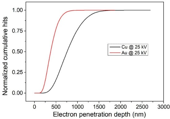
Figure 14.
Penetration depth of electrons with an energy of 25 keV in copper and gold.
The EPMA detector is present as an upgrade of conventional SEM, but most of the instruments come at least with the EDS detector by default. The electron bombardment of the beam excites the atoms in the sample, knocking out the electrons from the inner shells. Such a state is unstable, and the resulting electron-hole is immediately filled by a higher-energy electron from a higher atomic orbital. The energy difference is released in the form of an X-ray quantum. The resulting X-ray radiation is characteristic of the transition and the atom. For a single element, different transitions are allowed, depending on which shell the higher-energy electron comes from and which shell the hole must filled in. This results in X-ray quanta, which are marked with Kα, Kβ, Lα, etc. The energy of X-ray lines (position of the lines in the spectrum) is an indicator of which element is under investigation. The intensity of the line depends on the concentration of the element within the sample. Furthermore, the electrons, slowing down in the electric field of the atomic nuclei, generate an X-ray braking radiation, called bremsstrahlung, which constitutes the continuous background of the EPMA spectrum. The EPMA detector exploits the energy interaction between X-rays and suitable material, generally represented by a single silicon crystal doped with lithium, coated at both ends with a gold conductive layer, at a temperature of −192 °C with liquid nitrogen. Other variants are the high purity germanium detectors and silicon drift detector (SSD) with Peltier cooling. When an X-ray photon is absorbed in the sensitive area of the detector, then electron–hole pairs are produced, which causes the production of an electric current, which is then sensitively amplified. WDS instruments present a diffracting crystal that selects the photons to be sent to the detector, which measures only the number of pulses, i.e., photons. In the EDS system, there is not a photon selector; thus, the signal of each photon is processed to obtain its energy value; during this time, the system rejects every other signal, resulting in a dead time. High dead time produces high spectra with high resolution but a low signal, because many photons are rejected; on the other hand, low dead time produces a high signal but wide peaks. A longer process time is needed for quantitative analysis where spectral resolution is important, whereas if maximizing the number of X-rays in a spectrum or map is most important, a shorter process time can be used. Si (Li) detectors operate at count rates of about 1 to 20 kCPS with optimal dead times of 20%–30%. The reason why SDD is now preferred to Si (Li) detectors is that they can handle much higher count rates of >100 kCPS and dead times of 50%. The count rate can be optimized by adjusting the beam current (probe current or spot size) and the processing time. It is important to select a processing time and beam current that will give an acceptable X-ray count rate and detector dead time for analysis, as well as the desired spectral resolution. The typical energy resolution of an EDS detector is 130–140 eV, while it is less than about 10 eV for WDS systems. Moreover, EDS systems have much lower count rates and poor reproducibility, generally by a factor of ten, with respect to WDS detectors. The beam energy can be varied to increase sensitivity for thinner or thicker coatings (Figure 15).
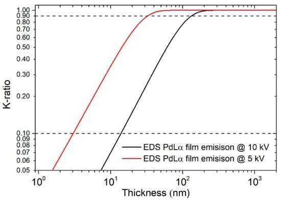
Figure 15.
Log–log plot of the emission of Pd film on Cu as a function of the thickness using a 5 and 10 kV electron beam. The 10%–90% thickness range is marked.
The film thickness can be obtained from the measured spectra through various approaches. The calibration curve can be obtained using standards of known thickness [157] or Monte Carlo simulations [20,21]. In terms of the quantification method, the quantity used in the calibration curves, multiple alternatives were evaluated: the K-ratio [153,158,159,160], which is the ratio between the intensity in the sample and the intensity in a standard with known composition, commonly used in quantification; the ratio of intensities [161]; and the atomic ratio [157], obtained performing the ZAF correction algorithm on the K-ratios. Both the absolute thickness [162,163] as well the mass thickness [164,165,166,167] were taken into consideration for the quantification.
In the last fifty years, many software programs were written to simulate EDS spectra [168]; many of them were written by researchers, and some were commercial: MAGIC [169,170], STRATAGEM [171,172,173], GMRFILM [148], Electron Flight Simulator [174,175], ThinFilmID [176], LayerProbe [176,177], pyPENELOPE [178,179], Win X-ray [180,181], MC X-ray [180,182], XFilms [183], CASINO [150,184,185,186,187], CalcZAF [188,189] and DTSA-II [190,191,192]. Many of these softwares exploit the PENEPMA algorithm [179]. PENEPMA is a simplified version dedicated to EPMA, written to perform simulation of X-ray spectra and calculate different quantities of interest of another algorithm called PENELOPE. PENELOPE (penetration and energy loss of positrons and electrons) is a general-purpose Monte Carlo code system for the simulation of coupled electron–photon transport in arbitrary materials. PENELOPE covers the energy range from 1 GeV down to, nominally, 50 eV. The physical interaction models implemented in the code are based on the most reliable information available at present, limited only by the required generality of the code. These models combine results from first-principles calculations, semi-empirical models and evaluated databases. It should be borne in mind that although PENELOPE can run particles down to 50 eV, the interaction cross-sections for energies below 1 keV may be affected by sizeable uncertainties; the results for these energies should be considered as semi-quantitative. PENELOPE incorporates a flexible geometry package called PENGEOM that permits automatic tracking of particles in complex geometries consisting of homogeneous bodies limited by quadratic surfaces. The PENELOPE code system is distributed by the OECD/NEA data bank. The distribution package includes a report [193] that provides detailed information on the physical models and random sampling algorithms adopted in PENELOPE, on the PENGEOM geometry package, and on the structure and operation of the simulation routines. PENELOPE is coded as a set of FORTRAN subroutines, which perform the random sampling of interactions and the tracking of particles (either electrons, positrons or photons). In principle, the user should provide the main steering program to follow the particle histories through the material structure and to keep scores of quantities of interest. In PENEPMA, photon interactions are simulated in chronological succession, allowing the calculation of X-ray fluorescence in complex geometries. PENEPMA makes extensive use of interaction forcing (a variance-reduction technique that artificially increases the probability of occurrence of relevant interactions) to improve the efficiency. CalcZAF [188] simulation software is based on PENEPMA and is a general-purpose software package for simulation of both relativistic and sub relativistic electron interactions with matter. Even in this case, the characteristics and the geometry of the detector are not taken into account, and the output consists of a lines-like unconvoluted spectrum. DTSA-II [190] shares many physical models with PENEPMA but was designed exclusively for simulation of X-ray spectra generated by sub relativistic electrons. DTSA2 uses variance reduction techniques unsuited to general-purpose code. These optimizations help the program to be orders of magnitude more computationally efficient while retaining the detector position sensitivity. Simulations are executed in minutes rather than hours, and differences that result from varying the detector position can be modelled. It is possible to insert the characteristics and the geometry of the detector in DTSA2, which is capable of handling complex sample geometries. The primary and secondary bremsstrahlung and fluorescence can be calculated. The outputs consist of a real-looking spectrum, since it is deconvoluted considering the detector resolution; even the electron trajectories can be visualized. CASINO [184] is single scattering Monte Carlo simulation software of electron trajectory in solids specifically designed for low beam interactions in a bulk and thin foil. This software can be used to generate many of the recorded signals (X-rays and backscattered electrons) in a scanning electron microscope. This program can also be efficiently used for all the accelerated voltage found on a field emission scanning electron microscope (0.1 to 30 keV). The characteristics and the geometry of the detector are not taken into account, and the output is not a spectrum but rather the characteristic emission line intensities as a function of the depth.
The X-ray depth distribution of the emissions is described by the φ (ρz) curve, which can be used for the determination of thin film thicknesses [13]. The thickness of the film can vary between two extremes relative to the curve: extremely thin or extremely thick [163]. In the first case, the emission corresponds to a bulk sample with the composition of the substrate, and in the second case, to a bulk sample with the composition of the film. In the intermediate cases, the φ (ρz) curves vary between these two extremes. The maximum thickness that can be analyzed with the EPMA method is in the order of microns; this is determined by the acceleration potential of the electrons together with the atomic number of the elements in the sample [194]. On the other hand, the minimum detectable thickness (lower detection limit) is given by the combination of the X-ray energy characteristics of the elements in the sample and the properties of the detector and can be as low as a few monolayers or less [195].
Exploiting STRATAGEM software, Kühn [172] was capable of obtaining both the elemental composition and thickness of the thin film ternary alloy, Pd–Ni–Co, co-deposited via magnetron sputtering on a silicon wafer by ED-EPMA in the range of 50 to 250 nm. The results were confirmed by AES and XPS measurement, for the composition, and by SEM imaging for the thickness. CASINO simulations confirmed the volume of interaction. A similar approach was used for the determination of electrodeposited Ni, Pd and Au on Cu, comparing the results of CASINO, CalcZAF and DTSA [19]. A comparison between GRMfilm, DTSA-II and PENEPMA was performed for very thin films (5–20 m) of Al and Cu on Bi; in this study, also the variation in the film density with respect to the bulk material was evaluated [196]. Ultra-thin films of Ge, Sn, Ag and Au on Si wafer were also evaluated by Campos performing multiple analyses with different beam energies [197]. DTSA-II was also used to determine the sputter coated deposition of Ti and Ag on Si for medical applications [198]. Osada [162] developed new MC simulation software to evaluate the thickness of aluminum oxide on aluminum sheets in the range of 5 to 50 nm. Recently, in 2018, Darznek performed thickness measurement, tilting the sample off the normal incidence angle to increase the signal of the superficial coatings, precisely to determine the thickness of chromium film on a silicon substrate. With this approach, he was able to determine up to 1014 atoms per square centimeter, with an error of less than 10%, exploiting K-ratio measurement with MC simulation.
In 2016, Sokolov [150] measured the thickness of silicon dioxide and silicon nitride thin films using EDS, varying the penetration depth of the analysis, changing the acceleration voltage of the beam and correlating the thickness of the film with the signal of the substrate elements to the collected noise. Stanford [199], in 2020, measured the oxide layer formation on Pu from 35 to 400 nm using measured standards to build the k-ratio calibration curves of oxygen through FIB-SEM analysis. Previously Bastin made a massive work collecting the K-ratio of Al [200] and Pd [201] of films from 10 to 320 nm in thickness at various beam energies between 3 and 30 kV on many substrates between Be and Bi.
Even the thickness of multi-layered samples can be measured using EPMA measurements [202,203]. In 2019, Pazzaglia [204] developed a new model for the standardless determination of mass thickness and composition using EDS for multilayer samples with an accuracy of 10 μg/cm2. Previously, Lesch used a sputtering method with EPMA, where the signal deconvolution with max entropy algorithm provided the thickness of Ti/Al/Ti layers deposited on Si.
EPMA was used by some authors to evaluate critical information about layered samples besides their thickness. Christien [145] used EDS measurement to determine the interdiffusion coefficient between thin films of miscible metals. Using various annealing temperature and Fick’s diffusion equations, he was able to estimate the coefficients for an Ni film on Pd. Darznek [205] proposed a method to evaluate thickness uniformity of nanofilms by means of MC simulations, correlating the intensities of the peaks in the EDS spectrum to the film thickness. In 2016, Ortel [142] developed a technique combining EPMA measurement for mass deposition determination and SEM analysis for thickness determination to obtain the change in density of the films with respect to the bulk materials and consequently extrapolate the porosity of the coatings.
3.3. Ellipsometry
Ellipsometry is a non-destructive optical technique that enables one to determine the optical constants, the microstructure and the thickness of thin films [206]. At its core, this method is based on the reflection of a linearly polarized light beam on the sample surface. The reflected light becomes elliptically polarized by interference, due to changes in phase and intensity with respect to the incident photons [207,208,209]. Ellipsometry in fact exploits the reflection/refraction of light that occurs at the boundary between two different materials. When a photon flux hits the surface of a thin film, part of it will be reflected, and part will be refracted at a different angle inside the material. This process also occurs at the boundary between the thin film and the bulk material underneath, giving rise to interference between the surface-reflected and the bulk-reflected light. These interference patterns can be fitted to a model in order to extract various parameters, among them, the film thickness and film roughness. The analysis process can be quite complex, especially for multi-layered materials.
This technique exploits the penetrating power of visible light, usually produced by a laser, in the matter. Light has to travel down to the substrate to acquire thickness-sensitive data. For this reason, it is particularly suited for transparent films, where it can be used to determine thicknesses up to a few microns. This leads to a significant limitation in the determination of metallic film thickness. Due to the high light absorption coefficient of metals in a vast portion of the spectra, it is nearly impossible to use this technique for layers thicker than 100 nm [207].
3.4. Rutherford Backscattering Spectroscopy
Rutherford backscattering spectroscopy permits the depth profiling and thickness determination of metallic thin films up to a few microns. This method exploits the elastic backscattering of an energetic beam of ions (usually He2+, reaching energies from 2 to 4 MeV) from the atom nuclei composing the target sample [30,210,211]. Resulting ions are analyzed by energy and by backscattering angle. The obtained spectra can be then fitted using programs like SIMNRA [212] or SRIM [213] in order to obtain film thicknesses.
This technique permits very fast acquisition times (less than ten minutes) on conducting, semiconducting or insulating thin films, without the use of standards, with thicknesses ranging from 5 to 7 microns to nanometers. The main limitation in its use is related to the need for a linear particle accelerator, which is costly and difficult to find in most service facilities. Moreover, the technique is not very sensitive to low-density atoms (below Ne) and to stacks of different layers. Samples have to be kept in ultra-high vacuum for the operations. In the end, the density of the film has to be known precisely in order to quantify the thickness correctly by the fitting of the experimental data using models.
3.5. Resonant Methods
3.5.1. Mechanical Resonance
Resonant techniques allow the characteristics of a film to be evaluated by observing the variation in the resonance frequency of mechanical oscillation or electromagnetic radiation. Using vibrating doubly clamped micro or nano-beams, the elastic modulus and density or thickness of an ultra-thin film can be obtained, and even the residual stress can be calculated [214,215,216]. The presence of a thin layer coating deposited on an elastic substrate generates stress and alters the elastic resonance properties of the latter. The film can be metallic, polymeric or of other nature. This is possible by measuring the dependence of the resonant frequency on the tension parameter as a result of in-plane and out-of-plane vibrations. To perform these measurements, it is necessary that the substrate has peculiar geometric characteristics. Therefore, the film must be specially deposited on the measuring base, and films on bulk samples cannot be analyzed. With this technique it is possible to measure films that have a thickness from a few nanometers to several microns. Using the same principle, cantilevers can also be used [217,218,219]. The cantilevers can be made using silicon properly oxidized by photolithography; the oxide regions can then be removed by hydrofluoric acid, leaving only the silicon cantilever [220].
3.5.2. Electromagnetic Resonance
Electromagnetic radiation can also be used to determine the thickness of a film by exploiting the resonance frequencies using both microwaves [221] and visible light [222,223]. Surface plasmon resonance (SPR) is a widely used technique in chemistry and biology to detect changes on the surface of the metal substrate, correlating them to the concentration of an analyte. The technique is based on the collective oscillations of free electrons, called surface plasmons, that can be optically excited by the attenuated total reflection under resonant conditions. The surface plasmon field decays exponentially away from the surface. The resonance condition is extremely sensitive to changes in the refractive index of the surrounding medium, which is influenced by the chemical environment on the surface. In the resonant condition, the decrease in the power of the reflected light is observed. This phenomenon can also be exploited to determine the thickness of films that change the SPR properties of the substrate [224,225]. Given the exponential decay of the superficial plasmon, thicknesses in the order of nanometers can be measured with this technique.
4. Conclusions
Thickness measurement is a challenge that affects many scientists and technicians, in both academic and industrial environments. The composite materials on which metallic coatings are applied are ubiquitous and allow one to obtain properties that a single element would not have. Thickness control is decisive for the obtainment of definite technological properties, and thus its measurement is necessary. In this review, we described the primary techniques, both for preparation and analysis, which are used both in research and in the industrial sector for this purpose. In fact, there is no perfect technique suitable for any type of sample, but the most appropriate route must be chosen for every need. At the end of this work, it seems reasonable to report a rough comparison between the various methods as regards the range of thicknesses that can be analyzed (Figure 16) and the times required to carry out the analysis (Figure 17). The costs are also an important parameter to consider, and they are very variable; from a general point of view, mechanical and optical techniques are cheaper than electronic, ionic and spectroscopic techniques. It should also be taken into account that some instruments are supplied with multiple combined analyzers, such as in the case of SE, BSE and EDS or for FIB techniques.
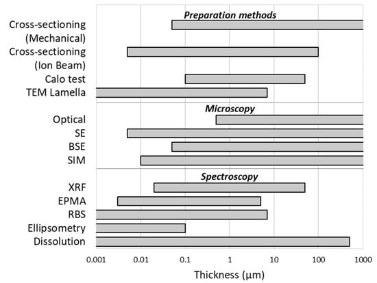
Figure 16.
Range of thicknesses that a metal sample must have to be properly analyzed for each technique.
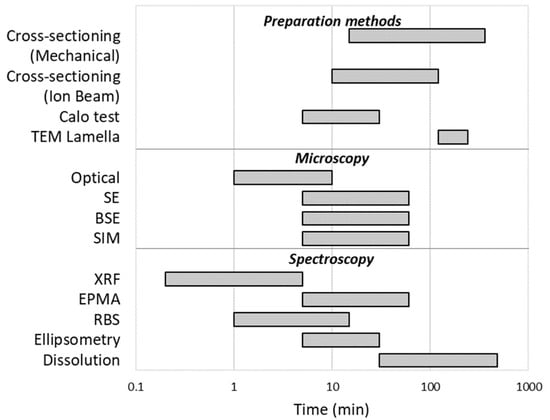
Figure 17.
Time needed for the measurement and preparation of a sample for each technique.
In terms of the measurable ranges of thicknesses, microscopic techniques tend to have only a lower limit, dictated by the aberrations that the beam undergoes under certain dimensions, while it is possible to lower the magnifications until observing shapes above the millimeter. Spectroscopic techniques instead suffer from the attenuation of the signal inside the sample and therefore cannot measure coatings beyond a certain size, which appear as infinitely thick. Furthermore, for those analysis techniques that require sample preparation, the range that can be analyzed is the intersection of the ranges of the individual techniques.
Considering now the preparation and measurement time, it is highly dependent on the presence of automated systems and on the experience and manual skills of the operator, as well as on the degree of accuracy required for the result. In general, the XRF, in addition to being extremely versatile, is the fastest technique, not even requiring sample preparation. On the other hand, microscopic techniques coupled with cross-sectioning are widespread, as they allow a result in which the thickness is directly visible to be obtained. Furthermore, cross-sectioning, although time-consuming, is a procedure that is generally automated.
Some of the illustrated techniques are well established and have not undergone many innovations in recent years, if not engineering optimization of performance and costs; for others, however, research is still very active, as we have shown in this work. Therefore, they must be followed with interest in order to make the best use of them as the powerful analytical tools that they are.
Author Contributions
Writing—original draft preparation, W.G. and E.B.; writing—review and editing, W.G. and E.B.; supervision, A.L. and M.I.; project administration, A.L. and M.I.; funding acquisition, A.L. and M.I. All authors have read and agreed to the published version of the manuscript.
Funding
This research was funded by the PRIN (“Progetti di Ricerca di Rilevante Interesse Nazionale”), which made possible the project “Novel Multilayered and Micro-Machined Electrode Nano-Architectures for Electrocatalytic Applications (Fuel Cells and Electrolyzers)”, grant number 2017YH9MRK. The authors also acknowledge “Ente Cassa di Risparmio di Firenze”, grant number 2013.0878, and Regione Toscana POR FESR 2014–2020 for the project FELIX (Fotonica ed Elettronica Integrate per l’Industria), grant number 6455.
Conflicts of Interest
The authors declare no conflict of interest.
References
- Whiteside, P.; Chininis, J.; Hunt, H. Techniques and challenges for characterizing metal thin films with applications in photonics. Coatings 2016, 6, 35. [Google Scholar] [CrossRef]
- Nash, C.R.; Fenton, J.C.; Constantino, N.G.N.; Warburton, P.A. Compact chromium oxide thin film resistors for use in nanoscale quantum circuits. J. Appl. Phys. 2014, 116. [Google Scholar] [CrossRef]
- Lobo, R.F.M.; Pereira-da-Silva, M.A.; Raposo, M.; Faria, R.M.; Oliveira, O.N. In situ thickness measurements of ultra-thin multilayer polymer films by atomic force microscopy. Nanotechnology 1999, 10, 389–393. [Google Scholar] [CrossRef]
- Sitko, R. Quantitative X-ray fluorescence analysis of samples of less than “infinite thickness”: Difficulties and possibilities. Spectrochim. Acta Part B At. Spectrosc. 2009, 64, 1161–1172. [Google Scholar] [CrossRef]
- Lopes, F.; Cardozo Amorin, L.H.; da Silva Martins, L.; Urbano, A.; Roberto Appoloni, C.; Cesareo, R. Thickness measurement of V2O5 nanometric thin films using a portable XRF. J. Spectrosc. 2016, 2016, 1–7. [Google Scholar] [CrossRef]
- Criss, J.W.; Birks, L.S. Calculation methods for fluorescent X-ray spectrometry: Empirical coefficients vs. fundamental parameters. Anal. Chem. 1968, 40, 1080–1086. [Google Scholar] [CrossRef]
- Giurlani, W.; Berretti, E.; Lavacchi, A.; Innocenti, M. Thickness determination of metal multilayers by ED-XRF multivariate analysis using Monte Carlo simulated standards. Anal. Chim. Acta 2020, 1130, 72–79. [Google Scholar] [CrossRef] [PubMed]
- Giurlani, W.; Berretti, E.; Innocenti, M.; Lavacchi, A. Coating Thickness determination using X-ray fluorescence spectroscopy: Monte Carlo simulations as an alternative to the use of standards. Coatings 2019, 9, 79. [Google Scholar] [CrossRef]
- Pessanha, S.; Manso, M.; Antunes, V.; Carvalho, M.L.; Sampaio, J.M. Monte Carlo simulation of portable X-ray fluorescence setup: Non-invasive determination of gold leaf thickness in indo-Portuguese panel paintings. Spectrochim. Acta Part B At. Spectrosc. 2019, 156, 1–6. [Google Scholar] [CrossRef]
- Malarde, D.; Powell, M.J.; Quesada-Cabrera, R.; Wilson, R.L.; Carmalt, C.J.; Sankar, G.; Parkin, I.P.; Palgrave, R.G. Optimized atmospheric-pressure chemical vapor deposition thermochromic VO2 thin films for intelligent window applications. ACS Omega 2017, 2, 1040–1046. [Google Scholar] [CrossRef]
- Krumrey, M.; Gleber, G.; Scholze, F.; Wernecke, J. Synchrotron radiation-based X-ray reflection and scattering techniques for dimensional nanometrology. Meas. Sci. Technol. 2011, 22. [Google Scholar] [CrossRef]
- Serafińczuk, J.; Pietrucha, J.; Schroeder, G.; Gotszalk, T.P. Thin film thickness determination using X-ray reflectivity and Savitzky-Golay algorithm. Opt. Appl. 2011, 41, 315–322. [Google Scholar]
- Sokolov, S.A.; Milovanov, R.A.; Sidorov, L.N. Determination of the thickness of thin films based on scanning electron microscopy and energy dispersive X-ray analysis. J. Surf. Investig. X-ray Synchrotron Neutron Tech. 2019, 13, 836–847. [Google Scholar] [CrossRef]
- Goldstein, J.I.; Newbury, D.E.; Michael, J.R.; Ritchie, N.W.M.; Scott, J.H.J.; Joy, D.C. Scanning Electron Microscopy and X-ray Microanalysis; Springer Publishing: New York, NY, USA, 2018; ISBN 978-1-4939-6674-5. [Google Scholar]
- Jablonski, A. Evaluation of procedures for overlayer thickness determination from XPS intensities. Surf. Sci. 2019, 688, 14–24. [Google Scholar] [CrossRef]
- Walton, J.; Alexander, M.R.; Fairley, N.; Roach, P.; Shard, A.G. Film thickness measurement and contamination layer correction for quantitative XPS. Surf. Interface Anal. 2016, 48, 164–172. [Google Scholar] [CrossRef]
- Cumpson, P.J. The thickogram: A method for easy film thickness measurement in XPS. Surf. Interface Anal. 2000, 29, 403–406. [Google Scholar] [CrossRef]
- Alexander, M.R.; Thompson, G.E.; Zhou, X.; Beamson, G.; Fairley, N. Quantification of oxide film thickness at the surface of aluminium using XPS. Surf. Interface Anal. 2002, 34, 485–489. [Google Scholar] [CrossRef]
- Giurlani, W.; Innocenti, M.; Lavacchi, A. X-ray microanalysis of precious metal thin films: Thickness and composition determination. Coatings 2018, 8, 84. [Google Scholar] [CrossRef]
- Kyser, D.F.; Murata, K. Quantitative Electron Microprobe Analysis of Thin Films on Substrates. IBM J. Res. Dev. 1974, 92, 352–363. [Google Scholar] [CrossRef]
- Roming, A.D.; Plimpton, S.J.; Michael, J.R.; Myklebust, R.L. Newbury DE Microbeam Analysis; San Francisco Press: San Francisco, CA, USA, 1990. [Google Scholar]
- Hill, J.M.; Royce, D.G.; Fadley, C.S.; Wagner, L.F.; Grunthaner, F.J. Properties of oxidized silicon as determined by angular-dependent X-ray photoelectron spectroscopy. Chem. Phys. Lett. 1976, 44, 225–231. [Google Scholar] [CrossRef]
- Benoit, M.; Bataillon, C.; Gwinner, B.; Miserque, F.; Orazem, M.E.; Sánchez-Sánchez, C.M.; Tribollet, B.; Vivier, V. Comparison of different methods for measuring the passive film thickness on metals. Electrochim. Acta 2016, 201, 340–347. [Google Scholar] [CrossRef]
- Passiu, C.; Rossi, A.; Weinert, M.; Tysoe, W.; Spencer, N.D. Probing the outermost layer of thin gold films by XPS and density functional theory. Appl. Surf. Sci. 2020, 507, 145084. [Google Scholar] [CrossRef]
- Tougaard, S. Surface nanostructure determination by X-ray photoemission spectroscopy peak shape analysis. J. Vac. Sci. Technol. A Vac. Surf. Film 1996, 14, 1415–1423. [Google Scholar] [CrossRef]
- Matthew, J. Surface analysis by Auger and X-ray photoelectron spectroscopy. D. Briggs and J. T. Grant (eds). IMPublications, Chichester, UK and SurfaceSpectra, Manchester, UK, 2003. 900 pp., ISBN 1-901019-04-7, 900 pp. Surf. Interface Anal. 2004, 36, 1647. [Google Scholar] [CrossRef]
- Elsener, B.; Rossi, A. XPS investigation of passive films on amorphous FeCr alloys. Electrochim. Acta 1992, 37, 2269–2276. [Google Scholar] [CrossRef]
- Rossi, A.; Elsener, B. XPS analysis of passive films on the amorphous alloy Fe70Cr10P13C7: Effect of the applied potential. Surf. Interface Anal. 1992, 18, 499–504. [Google Scholar] [CrossRef]
- Asami, K.; Hashimoto, K. An XPS study of the surfaces on Fe–Cr, Fe–Co and Fe–Ni alloys after mechanical polishing. Corros. Sci. 1984, 24, 83–97. [Google Scholar] [CrossRef]
- Jeynes, C.; Colaux, J.L. Thin film depth profiling by ion beam analysis. Analyst 2016, 141, 5944–5985. [Google Scholar] [CrossRef]
- Ho, S.M. Investigation of the electrical properties of metal chalcogenide thin films: A review. Der Pharma Chem. 2016, 8, 17–20. [Google Scholar]
- Hofmann, S.; Zhou, G.; Kovac, J.; Drev, S.; Lian, S.Y.; Lin, B.; Liu, Y.; Wang, J.Y. Preferential sputtering effects in depth profiling of multilayers with SIMS, XPS and AES. Appl. Surf. Sci. 2019, 483, 140–155. [Google Scholar] [CrossRef]
- Bardi, U.; Caporali, S.; Chenakin, S.P.; Lavacchi, A.; Miorin, E.; Pagura, C.; Tolstogouzov, A. Characterization of electrodeposited metal coatings by secondary ion mass spectrometry. Surf. Coat. Technol. 2006, 200, 2870–2874. [Google Scholar] [CrossRef]
- Bardi, U.; Chenakin, S.P.; Ghezzi, F.; Giolli, C.; Goruppa, A.; Lavacchi, A.; Miorin, E.; Pagura, C.; Tolstogouzov, A. High-temperature oxidation of CrN/AlN multilayer coatings. Appl. Surf. Sci. 2005, 252, 1339–1349. [Google Scholar] [CrossRef]
- Kalina, L.; Bílek, V., Jr.; Bušo, M.; Koplík, J.; Másilko, J. Thickness determination of corrosion layers on iron using XPS depth profiling. Mater. Tehnol. 2018, 52, 537–540. [Google Scholar] [CrossRef]
- Scorciapino, M.A.; Navarra, G.; Elsener, B.; Rossi, A. Nondestructive surface depth profiles from angle-resolved X-ray photoelectron spectroscopy data using the maximum entropy method. I. A new protocol. J. Phys. Chem. C 2009, 113, 21328–21337. [Google Scholar] [CrossRef]
- Olla, M.; Navarra, G.; Elsener, B.; Rossi, A. Nondestructive in-depth composition profile of oxy-hydroxide nanolayers on iron surfaces from ARXPS measurement. Surf. Interface Anal. 2006, 38, 964–974. [Google Scholar] [CrossRef]
- Smith, G.C.; Livesey, A.K. Maximum entropy: A new approach to non-destructive deconvolution of depth profiles from angle-dependent XPS. Surf. Interface Anal. 1992, 19, 175–180. [Google Scholar] [CrossRef]
- Skilling, J.; Bryan, R.K. Maximum entropy image reconstruction: General algorithm. Mon. Not. R. Astron. Soc. 1984, 211, 111–124. [Google Scholar] [CrossRef]
- Wase, A.; Blann, G.; Crozet, D.; Danielczyk, T.; Didier, P.; Johnson, C.; Fisher, D.; Pascher, M.; Peters, D.; Garrett, L.; et al. The Sum of Our Experience a Guide to Materials Preparation & Analysis; Buehler: Lake Bluff, IL, USA, 2018; ISBN 0975289802. [Google Scholar]
- ISO 9220:1995—Metallic Coatings—Measurement of Coating Thickness—Scanning Electron Microscope Method; International Organization for Standardization: Geneva, Switzerland, 1995.
- ISO 1463:2004—Metallic and Oxide Coatings—Measurement of Coating Thickness—Microscopical Method; International Organization for Standardization: Geneva, Switzerland, 2004.
- ASTM B748-90 Standard Test Method for Measurement of Thickness of Metallic Coatings by Measurement of Cross Section with a Scanning Electron Microscope; International ASTM: West Conshohocken, PA, USA, 2001.
- Sohail, K.; Khan, I.U.; Shahzad, Y.; Hussain, T.; Ranjha, N.M. Ph-sensitive polyvinylpyrrolidone-acrylic acid hydrogels: Impact of material parameters on swelling and drug release. Braz. J. Pharm. Sci. 2014, 50, 173–184. [Google Scholar] [CrossRef]
- Gierak, J. Focused ion beam technology and ultimate applications. Semicond. Sci. Technol. 2009, 24. [Google Scholar] [CrossRef]
- Kleyn, A.W. Ion-Surface Interactions—From Channeling to Soft-Landing. Science 1997, 275, 1440–1441. [Google Scholar] [CrossRef]
- Huh, Y.; Hong, K.J.; Shin, K.S. Amorphization induced by focused ion beam milling in metallic and electronic materials. Microsc. Microanal. 2013, 19, 33–37. [Google Scholar] [CrossRef] [PubMed]
- Williams, J.S. Ion Implantation and Beam Processing; Elsevier: Amsterdam, The Netherlands, 1984; ISBN 9780127569802. [Google Scholar]
- MoberlyChan, W.J.; Adams, D.P.; Aziz, M.J.; Hobler, G.; Schenkel, T. Fundamentals of focused ion beam nanostructural processing: Below, at, and above the surface. MRS Bull. 2007, 32, 424–432. [Google Scholar] [CrossRef][Green Version]
- Ishitani, T.; Tsuboi, H. Objective comparison of scanning ion and scanning electron microscope images. Scanning 1997, 19, 489–497. [Google Scholar] [CrossRef]
- Tseng, A.A. Recent developments in micromilling using focused ion beam technology. J. Micromech. Microeng. 2004, 14. [Google Scholar] [CrossRef]
- Joo, S.; Liang, H. Secondary ION MASS SPECTROSCOPY (SIMS). In Encyclopedia of Tribology; Springer US: Boston, MA, USA, 2013; pp. 2989–2994. [Google Scholar]
- van Kouwen, L. Introduction to focused ion beams, ion sources, and the nano-aperture ion source. Adv. Imaging Electron Phys. 2019, 212, 181–216. [Google Scholar]
- Joy, D.C. SEM for the 21st century-scanning ion microscopy. Electron. Device Fail. Anal. 2012, 14, 4–12. [Google Scholar] [CrossRef][Green Version]
- Eder, K.; Bhatia, V.; Van Leer, B.; Cairney, J.M. Using a plasma FIB equipped with Xe, N2, O2 and Ar for atom probe sample preparation—Ion implantation and success rates. Microsc. Microanal. 2019, 25, 316–317. [Google Scholar] [CrossRef]
- Ernst, A.; Wei, M.; Aindow, M. A comparison of Ga FIB and Xe-plasma FIB of complex Al alloys. Microsc. Microanal. 2017, 23, 288–289. [Google Scholar] [CrossRef]
- Kant, K.; Losic, D. Focused ion beam (FIB) technology for micro- and nanoscale fabrications. In FIB Nanostructures; Wang, Z.M., Ed.; Springer: Heidelberg, Germany, 2013; Volume 20, pp. 1–22. [Google Scholar] [CrossRef]
- An, B.-S.; Kwon, Y.; Oh, J.-S.; Shin, Y.-J.; Ju, J.; Yang, C.-W. Evaluation of ion/electron beam induced deposition for electrical connection using a modern focused ion beam system. Appl. Microsc. 2019, 49. [Google Scholar] [CrossRef]
- Matsui, S. Encyclopedia of Nanotechnology; Bhushan, B., Ed.; Springer Netherlands: Dordrecht, The Netherlands, 2016; ISBN 978-94-007-6178-0. [Google Scholar]
- Randolph, S.J.; Fowlkes, J.D.; Rack, P.D. Focused, nanoscale electron-beam-induced deposition and etching. Crit. Rev. Solid State Mater. Sci. 2006, 31, 55–89. [Google Scholar] [CrossRef]
- Rai-Choudhury, P. Handbook of Microlithography, Micromachining, and Microfabrication, Volume 2: Micromachining and Microfabrication; SPIE Press: Bellingham, WA, USA, 1997; ISBN 9780819423795. [Google Scholar]
- Ishitani, T.; Yaguchi, T. Cross-sectional sample preparation by focused ion beam: A review of ion-sample interaction. Microsc. Res. Tech. 1996, 35, 320–333. [Google Scholar] [CrossRef]
- Mohamad Rashid, N.N.; Ahmad Junaidi, N.H.; Rahmah Aid, S. Interface damage of protective layer in TEM lamella preparation for highly doped Ge substrate. IOP Conf. Ser. Mater. Sci. Eng. 2019, 522, 012003. [Google Scholar] [CrossRef]
- Khamsehpour, B.; Davies, S.T. Angle lapping of multilayer structures for thickness measurements using focused ion beam micromachining. Semicond. Sci. Technol. 1994, 9, 249–255. [Google Scholar] [CrossRef]
- Gao, S.; Kang, R.K.; Guo, D.M.; Huang, Q.S. Study on the subsurface damage distribution of the silicon wafer ground by diamond wheel. Adv. Mater. Res. 2010, 126–128, 113–118. [Google Scholar]
- Mayer, J.; Giannuzzi, L.A.; Kamino, T.; Michael, J. TEM sample preparation and FIB-induced damage. MRS Bull. 2007, 32, 400–407. [Google Scholar] [CrossRef]
- Schaffer, M.; Schaffer, B.; Ramasse, Q. Sample preparation for atomic-resolution STEM at low voltages by FIB. Ultramicroscopy 2012, 114, 62–71. [Google Scholar] [CrossRef]
- ISO 26423:2009 Fine Ceramics (Advanced Ceramics, Advanced Technical Ceramics)—Determination of Coating Thickness by Crater-Grinding Method; ISO: Geneva, Switzerland, 2009.
- Vidakis, N.; Antoniadis, A.; Bilalis, N. The VDI 3198 indentation test evaluation of a reliable qualitative control for layered compounds. J. Mater. Process. Technol. 2003, 143–144, 481–485. [Google Scholar] [CrossRef]
- Randall, N. Finer particle size allows better coating characterization with the Calotest. Appl. Bull. 1997, 3–6. [Google Scholar]
- Demas, N.G.; Lorenzo-Martin, C.; Ajayi, O.O.; Erck, R.A.; Shareef, I. Measurement of thin-film coating hardness in the presence of contamination and roughness: Implications for tribology. Metall. Mater. Trans. A Phys. Metall. Mater. Sci. 2016, 47, 1629–1640. [Google Scholar] [CrossRef]
- Rupetsov, V.; Minchev, R. Experimental Calo Tester for the coating thickness measurement. In Proceedings of the XV International Scientific Conference, Smolyan, Bulgaria, 10–11 June 2016; pp. 188–192. [Google Scholar]
- Özkan, D.; Kaleli, H.; Yüksek, L. Quantitative comparison of tribological performance of chromium- and zinc-phosphate-coated piston rings in tribotest rig. Proc. Inst. Mech. Eng. Part J J. Eng. Tribol. 2017, 231, 75–92. [Google Scholar] [CrossRef]
- Škarohlíd, J.; Ashcheulov, P.; Škoda, R.; Taylor, A.; Čtvrtlík, R.; Tomáštík, J.; Fendrych, F.; Kopeček, J.; Cháb, V.; Cichoň, S.; et al. Nanocrystalline diamond protects Zr cladding surface against oxygen and hydrogen uptake: Nuclear fuel durability enhancement. Sci. Rep. 2017, 7, 6469. [Google Scholar] [CrossRef] [PubMed]
- Vieira Junior, L.E.; Bendo, T.; Nieto, M.I.; Klein, A.N.; Hotza, D.; Moreno, R.; Rodrigues Neto, J.B. Processing of Copper Based Foil Hardened with Zirconia by Non-Deformation Method. Mater. Res. 2017, 20, 835–842. [Google Scholar] [CrossRef][Green Version]
- Nyyssonen, D.; Kirk, C.P. Optical microscope imaging of lines patterned in thick layers with variable edge geometry: Theory. J. Opt. Soc. Am. A 1988, 5, 1270. [Google Scholar] [CrossRef]
- Sakai, Y.; Yamada, T.; Suzuki, T.; Ichinokawa, T. Contrast mechanisms of secondary electron images in scanning electron and ion microscopy. Appl. Surf. Sci. 1999, 144–145, 96–100. [Google Scholar] [CrossRef]
- Li, P.; Bao, S.X.; Zhang, D.Z.; Zhuang, L.B.; Ma, L.L. Application of secondary electron composition contrast imaging method in microstructure studies on cathode materials of TWT. Mater. Sci. Forum 2011, 689, 255–259. [Google Scholar]
- Tan, S.; Livengood, R.; Shima, D.; Notte, J.; McVey, S. Gas field ion source and liquid metal ion source charged particle material interaction study for semiconductor nanomachining applications. J. Vac. Sci. Technol. B Nanotechnol. Microelectron. Mater. Process. Meas. Phenom. 2010, 28, C6F15–C6F21. [Google Scholar] [CrossRef]
- Scipioni, L.; Stern, L.A.; Notte, J.; Sijbrandij, S.; Griffin, B. Helium ion microscope. Adv. Mater. Process. 2008, 166, 27–30. [Google Scholar] [CrossRef]
- Giannuzzi, L.A.; Michael, J.R. Comparison of channeling contrast between ion and electron images. Microsc. Microanal. 2013, 19, 344–349. [Google Scholar] [CrossRef]
- Twedt, K.A.; Chen, L.; McClelland, J.J. Scanning ion microscopy with low energy lithium ions. Ultramicroscopy 2014, 142, 24–31. [Google Scholar] [CrossRef]
- Postek, M.T.; Vladar, A.E.; Kramar, J.; Stern, L.A.; Notte, J.; McVey, S. Helium ion microscopy: A new technique for semiconductor metrology and nanotechnology. AIP Conf. Proc. 2007, 931, 161–167. [Google Scholar] [CrossRef]
- Passiu, C.; Rossi, A.; Bernard, L.; Paul, D.; Hammond, J.; Unger, W.E.S.; Venkataraman, N.V.; Spencer, N.D. Fabrication and microscopic and spectroscopic characterization of planar, bimetallic, micro- and nanopatterned surfaces. Langmuir 2017, 33, 5657–5665. [Google Scholar] [CrossRef] [PubMed]
- ISO 18516—Surface Chemical Analysis—Auger Electron Spectroscopy and X-ray Photoelectron Spectroscopy—Determination of Lateral Resolution; International Organization for Standardization: Geneva, Switzerland, 2006.
- Lee, D.H.; Cho, N.G. Assessment of surface profile data acquired by a stylus profilometer. Meas. Sci. Technol. 2012, 23. [Google Scholar] [CrossRef]
- Seo, Y.; Jhe, W. Atomic force microscopy and spectroscopy. Reports Prog. Phys. 2008, 71, 016101. [Google Scholar] [CrossRef]
- Eaton, P.; West, P. Atomic Force Microscopy; Oxford University Press: Oxford, UK, 2010; ISBN 9780199570454. [Google Scholar]
- Bramowicz, M.; Kulesza, S.; Rychlik, K. A Comparison between contact and tapping AFM mode in surface morphology studies. Tech. Sci. Univ. Warm. Maz. Olsztyn 2012, nr 15, 307–318. [Google Scholar]
- Werner, H.W. Theoretical and experimental ion mass spectrometry. Vacuum 1974, 24, 493–504. [Google Scholar] [CrossRef]
- Schaepe, K.; Jungnickel, H.; Heinrich, T.; Tentschert, J.; Luch, A.; Unger, W.E.S. Secondary ion mass spectrometry. Charact. Nanoparticles Meas. Process. Nanoparticles 2019, 481–509. [Google Scholar] [CrossRef]
- Matsuo, J.; Okubo, C.; Seki, T.; Aoki, T.; Toyoda, N.; Yamada, I. A new secondary ion mass spectrometry (SIMS) system with high-intensity cluster ion source. Nucl. Instruments Methods Phys. Res. Sect. B Beam Interact. Mater. Atoms 2004, 219–220, 463–467. [Google Scholar] [CrossRef]
- Moritani, K.; Hashinokuchi, M.; Nakagawa, J.; Kashiwagi, T.; Toyoda, N.; Mochiji, K. Extremely low-energy projectiles for SIMS using size-selected gas cluster ions. Appl. Surf. Sci. 2008, 255, 948–950. [Google Scholar] [CrossRef]
- Stevie, F.A.; Sedlacek, L.; Babor, P.; Jiruse, J.; Principe, E.; Klosova, K. FIB-SIMS quantification using TOF-SIMS with Ar and Xe plasma sources. Surf. Interface Anal. 2014, 46, 285–287. [Google Scholar] [CrossRef]
- D’Agostino, A.T. Determination of thin metal film thickness by X-ray diffractometry using the Scherrer equation, atomic absorption analysis and transmission/reflection visible spectroscopy. Anal. Chim. Acta 1992, 262, 269–275. [Google Scholar] [CrossRef]
- D’Agostino, A.T. A Multitechnique Approach for Materials Characterization: Using X-ray diffractometry, visible spectroscopy, and atomic absorption analysis to determine thin metal film thickness. J. Chem. Educ. 1994, 71, 892. [Google Scholar] [CrossRef]
- Lindner, M.; Höflsauer, F.; Heider, J.; Reinelt, M.; Langowski, H.-C. Comparison of thickness determination methods for physical-vapor-deposited aluminum coatings in packaging applications. Thin Solid Films 2018, 666, 6–14. [Google Scholar] [CrossRef]
- Szklarska, M.; Dercz, G.; Smołka, A.; Popczyk, M.; Łosiewicz, B. A Coulometric Method by local anodic dissolution for measuring the thickness of Ni/Cu multi-layer electrocoatings. Solid State Phenom. 2015, 228, 319–324. [Google Scholar]
- Bertorelle, E. Trattato di Galvanotecnica; Metallurgia e Siderurgia; Hoepli: Milan, Italy, 2016; ISBN 9788820374983. [Google Scholar]
- Giurlani, W.; Zangari, G.; Gambinossi, F.; Passaponti, M.; Salvietti, E.; Di Benedetto, F.; Caporali, S.; Innocenti, M. Electroplating for decorative applications: Recent trends in research and development. Coatings 2018, 8, 260. [Google Scholar] [CrossRef]
- Innocenti, M.; Giurlani, W.; Passaponti, M.; Luca, D.; Salvietti, E. Electrodeposition and innovative characterization of precious metal alloys for the Galvanic and Jewel industry. Substantia 2019, 3, 29–37. [Google Scholar] [CrossRef]
- ISO 3497:2000 Metallic Coatings—Measurement of Coating Thickness—X-ray Spectrometric Methods; International Organization for Standardization: Geneva, Switzerland, 2000.
- ASTM B568-98 Standard Test Method for Measurement of Coating Thickness by X-ray Spectrometry; International ASTM: West Conshohocken, PA, USA, 1998.
- Takahara, H. Thickness and composition analysis of thin film samples using FP method by XRF analysis. Rigaku J. 2017, 33, 17–21. [Google Scholar]
- Boehm, S.; Bügler, M.J.L. Layer Thickness Analysis of Thin Metal Coatings with micro-XRF on SEM; Bruker Nano Analytics: Berlin, Germany, 2017. [Google Scholar]
- Axic Inc. Non-Destructive Composition and Thickness Analysis of Metal Films Using Combination EDS/WDS X-ray Fluorescence Spectrometry; Axic Inc. Application Note; Axic Inc.: Milpitas, CA, USA, 1989. [Google Scholar]
- Brouwer, P. Theory of XRF—Getting Acquainted with the Principles; PANalytical BV: Almelo, The Netherland, 2010; ISBN 9090167587. [Google Scholar]
- Abdel-Fattah, T.M.; Wixtrom, A.; Arias, L.; Zhang, K.; Baumgart, H. Quantitative analysis of X-ray fluorescence absorption and emission for thickness determination of ALD-grown metal and oxide nanoscaled films. J. Nanosci. Nanotechnol. 2017, 17, 5745–5750. [Google Scholar] [CrossRef]
- Hamann, D.M.; Bardgett, D.; Cordova, D.L.M.; Maynard, L.A.; Hadland, E.C.; Lygo, A.C.; Wood, S.R.; Esters, M.; Johnson, D.C. Sub-monolayer accuracy in determining the number of atoms per unit area in ultrathin films using X-ray fluorescence. Chem. Mater. 2018, 30, 6209–6216. [Google Scholar] [CrossRef]
- Kataoka, Y. Standardless X-ray fluorescence spectrometry (fundamental parameter method using sensitivity library). Rigaku J. 1989, 6, 33–40. [Google Scholar]
- Thomsen, V. Basic fundamental parameters in X-ray fluorescence. Spectroscopy 2007, 22, 46–50. [Google Scholar]
- Han, X.Y.; Zhuo, S.J.; Shen, R.X.; Wang, P.L.; Ji, A. Comparison of the quantitative results corrected by fundamental parameter method and difference calibration specimens in X-ray fluorescence spectrometry. J. Quant. Spectrosc. Radiat. Transf. 2006, 97, 68–74. [Google Scholar] [CrossRef]
- Pessanha, S.; Fonseca, C.; Santos, J.P.; Carvalho, M.L.; Dias, A.A. Comparison of standard-based and standardless methods of quantification used in X-ray fluorescence analysis: Application to the exoskeleton of clams. X-ray Spectrom. 2018, 47, 108–115. [Google Scholar] [CrossRef]
- Nygård, K.; Hämäläinen, K.; Manninen, S.; Jalas, P.; Ruottinen, J.-P. Quantitative thickness determination using X-ray fluorescence: Application to multiple layers. X-ray Spectrom. 2004, 33, 354–359. [Google Scholar] [CrossRef]
- Vrielink, J.A.M.; Tiggelaar, R.M.M.; Gardeniers, J.G.E.; Lefferts, L. Applicability of X-ray fluorescence spectroscopy as method to determine thickness and composition of stacks of metal thin films: A comparison with imaging and profilometry. Thin Solid Films 2012, 520, 1740–1744. [Google Scholar] [CrossRef]
- Elam, W.T.T.; Shen, R.B.; Scruggs, B.; Nicolosi, J. Accuracy of standardless FP analysis of bulk and thin film samples using a new atomic database. Adv. X-ray Anal. 2004, 47, 104–109. [Google Scholar]
- Ager, F.J.; Ferretti, M.; Grilli, M.L.; Juanes, D.; Ortega-Feliu, I.; Respaldiza, M.A.; Roldán, C.; Scrivano, S. Reconsidering the accuracy of X-ray fluorescence and ion beam based methods when used to measure the thickness of ancient gildings. Spectrochim. Acta Part B At. Spectrosc. 2017, 135, 42–47. [Google Scholar] [CrossRef]
- Kolbe, M.; Beckhoff, B.; Krumrey, M.; Ulm, G. Thickness determination for Cu and Ni nanolayers: Comparison of completely reference-free fundamental parameter-based X-ray fluorescence analysis and X-ray reflectometry. Spectrochim. Acta Part B At. Spectrosc. 2005, 60, 505–510. [Google Scholar] [CrossRef]
- Queralt, I.; Ibañez, J.; Marguí, E.; Pujol, J. Thickness measurement of semiconductor thin films by energy dispersive X-ray fluorescence benchtop instrumentation: Application to GaN epilayers grown by molecular beam epitaxy. Spectrochim. Acta Part B At. Spectrosc. 2010, 65, 583–586. [Google Scholar] [CrossRef]
- XRMC. Available online: https://github.com/golosio/xrmc/wiki (accessed on 30 July 2020).
- XMI-MSIM. Available online: https://github.com/tschoonj/xmimsim/wiki (accessed on 30 July 2020).
- Xraylib. Available online: https://github.com/tschoonj/xraylib/wiki (accessed on 30 July 2020).
- Schoonjans, T.; Brunetti, A.; Golosio, B.; Sanchez Del Rio, M.; Solé, V.A.; Ferrero, C.; Vincze, L. The xraylib library for X-ray-matter interactions. Recent developments. Spectrochim. Acta Part B At. Spectrosc. 2011, 66, 776–784. [Google Scholar] [CrossRef]
- Golosio, B.; Schoonjans, T.; Brunetti, A.; Oliva, P.; Masala, G.L. Monte Carlo simulation of X-ray imaging and spectroscopy experiments using quadric geometry and variance reduction techniques. Comput. Phys. Commun. 2014, 185, 1044–1052. [Google Scholar] [CrossRef]
- Schiavon, N.; de Palmas, A.; Bulla, C.; Piga, G.; Brunetti, A. An energy-dispersive X-ray fluorescence spectrometry and Monte Carlo simulation study of iron-age nuragic small bronzes (“navicelle”) from Sardinia, Italy. Spectrochim. Acta Part B At. Spectrosc. 2016, 123, 42–46. [Google Scholar] [CrossRef]
- Brunetti, A.; Fabian, J.; La Torre, C.W.; Schiavon, N. A combined XRF/Monte Carlo simulation study of multilayered peruvian metal artifacts from the tomb of the priestess of chornancap. Appl. Phys. A 2016, 122, 571. [Google Scholar] [CrossRef]
- Bottaini, C.E.; Brunetti, A.; Montero-Ruiz, I.; Valera, A.; Candeias, A.; Mirão, J. Use of Monte Carlo simulation as a tool for the nondestructive energy dispersive X-ray fluorescence (ED-XRF) spectroscopy analysis of archaeological copper-based artifacts from the chalcolithic site of perdigões, Southern Portugal. Appl. Spectrosc. 2018, 72, 17–27. [Google Scholar] [CrossRef] [PubMed]
- Barcellos Lins, S.A.; Ridolfi, S.; Gigante, G.E.; Cesareo, R.; Albini, M.; Riccucci, C.; di Carlo, G.; Fabbri, A.; Branchini, P.; Tortora, L. Differential X-ray attenuation in MA-XRF analysis for a non-invasive determination of gilding thickness. Front. Chem. 2020, 8, 1–9. [Google Scholar] [CrossRef] [PubMed]
- Cesareo, R. Gold, gildings, and tumbaga from the Moche tomb of the Lady of Cao: An EDXRF test for the internal ratio method. X-ray Spectrom. 2019, 48, 202–207. [Google Scholar] [CrossRef]
- Cesareo, R.; Franco Jordan, R.; Fernandez, A.; Bustamante, A.; Fabian, J.; del Pilar Zambrano, S.; Azeredo, S.; Lopes, R.T.; Ingo, G.M.; Riccucci, C.; et al. Analysis of the spectacular gold and silver from the Moche tomb ‘Señora de Cao’. X-ray Spectrom. 2016, 45, 138–154. [Google Scholar] [CrossRef]
- Cesareo, R.; de Assis, J.T.; Roldán, C.; Bustamante, A.D.; Brunetti, A.; Schiavon, N. Multilayered samples reconstructed by measuring Kα/Kβ or Lα/Lβ X-ray intensity ratios by EDXRF. Nucl. Instruments Methods Phys. Res. Sect. B Beam Interact. Mater. Atoms 2013, 312, 15–22. [Google Scholar] [CrossRef]
- Cesareo, R.; Bustamante, A.; Fabian, J.; Calza, C.; Dos Anjos, M.; Lopes, R.T.; Elera, C.; Shimada, I.; Curay, V.; Rizzutto, M.A. Energy-dispersive X-ray fluorescence analysis of a pre-Columbian funerary gold mask from the Museum of Sicán, Peru. X-ray Spectrom. 2010, 39, 122–126. [Google Scholar] [CrossRef]
- Cesareo, R. Non-destructive EDXRF-analysis of the golden haloes of Giotto’s frescos in the Chapel of the Scrovegni in Padua. Nucl. Instruments Methods Phys. Res. Sect. B Beam Interact. Mater. Atoms 2003, 211, 133–137. [Google Scholar] [CrossRef]
- Barcellos Lins, S.A.; Gigante, G.E.; Cesareo, R.; Ridolfi, S.; Brunetti, A. Testing the Accuracy of the calculation of gold leaf thickness by MC simulations and MA-XRF scanning. Appl. Sci. 2020, 10, 3582. [Google Scholar] [CrossRef]
- Porcinai, S.; Ferretti, M. X-ray fluorescence-based methods to measure the thickness of protective organic coatings on ancient silver artefacts. Spectrochim. Acta Part B At. Spectrosc. 2018, 149, 184–189. [Google Scholar] [CrossRef]
- de Almeida, E.; Melquiades, F.L.; Marques, J.P.R.; Marguí, E.; de Carvalho, H.W.P. Determination of the polymeric thin film thickness by energy dispersive X-ray fluorescence and multivariate analysis. Spectrochim. Acta Part B At. Spectrosc. 2020, 167, 105818. [Google Scholar] [CrossRef]
- West, M.; Ellis, A.T.; Streli, C.; Vanhoof, C.; Wobrauschek, P. 2017 atomic spectrometry update–a review of advances in X-ray fluorescence spectrometry and its special applications. J. Anal. At. Spectrom. 2017, 32, 1629–1649. [Google Scholar] [CrossRef]
- Vanhoof, C.; Bacon, J.R.; Ellis, A.T.; Vincze, L.; Wobrauschek, P. 2018 atomic spectrometry update–a review of advances in X-ray fluorescence spectrometry and its special applications. J. Anal. At. Spectrom. 2018, 33, 1413–1431. [Google Scholar] [CrossRef]
- Vanhoof, C.; Bacon, J.R.; Ellis, A.T.; Fittschen, U.E.A.; Vincze, L. 2019 atomic spectrometry update–a review of advances in X-ray fluorescence spectrometry and its special applications. J. Anal. At. Spectrom. 2019, 34, 1750–1767. [Google Scholar] [CrossRef]
- Castaing, R. Application of Electron Probes to Local Chemical and Crystallographic Analysis. Ph.D. Thesis, University of Paris, Paris, France, 1951. [Google Scholar]
- Richter, S.; Pinard, P.T. Combined EPMA, FIB and Monte Carlo simulation: A versatile tool for quantitative analysis of multilayered structures. IOP Conf. Ser. Mater. Sci. Eng. 2016, 109, 012014. [Google Scholar] [CrossRef]
- Ortel, E.; Hertwig, A.; Berger, D.; Esposito, P.; Rossi, A.M.A.M.; Kraehnert, R.; Hodoroaba, V.-D. New approach on quantification of porosity of thin films via electron-excited X-ray spectra. Anal. Chem. 2016, 88, 7083–7090. [Google Scholar] [CrossRef]
- Eggert, F. EDX-spectra simulation in electron probe microanalysis. Optimization of excitation conditions and detection limits. Microchim. Acta 2006, 155, 129–136. [Google Scholar] [CrossRef]
- Armigliato, A. Thin film X-ray microanalysis with the analytical electron microscope. J. Anal. At. Spectrom. 1999, 14. [Google Scholar] [CrossRef]
- Christien, F.; Pierson, J.F.; Hassini, A.; Capon, F.; Le Gall, R.; Brousse, T. EPMA–EDS surface measurements of interdiffusion coefficients between miscible metals in thin films. Appl. Surf. Sci. 2010, 256, 1855–1860. [Google Scholar] [CrossRef]
- Pascual, R.; Cruz, L.R.R.; Ferreira, C.L.L.; Gomes, D.T.T. Thin film thickness measurement using the energy-dispersive spectroscopy technique in a scanning electron microscope. Thin Solid Films 1990, 185, 279–286. [Google Scholar] [CrossRef]
- Benoit, D.; Bresse, J.-F.; Van’t dack, L.; Werner, H.; Wernisch, J. (Eds.) Microbeam and Nanobeam Analysis; Springer Vienna: Vienna, Austria, 1996; ISBN 978-3-211-82874-8. [Google Scholar]
- Waldo, R.A.; Militello, M.C.; Gaarenstroom, S.W. Quantitative thin-film analysis with an energy-dispersive X-ray detector. Surf. Interface Anal. 1993, 20. [Google Scholar] [CrossRef]
- Gauvin, R. Quantitative X-ray microanalysis of heterogeneous materials using Monte Carlo simulations. Microchim. Acta 2006, 155. [Google Scholar] [CrossRef]
- Sokolov, S.A.; Kelm, E.A.; Milovanov, R.A.; Abdullaev, D.A.; Sidorov, L.N. Non-destructive determination ofthickness of the dielectric layers using EDX. Proc. SPIE Int. Soc. Opt. Eng. 2016, 10224, 1022426. [Google Scholar] [CrossRef]
- Stenberg, G.; Boman, M. Thickness measurement of light elemental films. Diam. Relat. Mater. 1996, 5, 1444–1449. [Google Scholar] [CrossRef]
- Willich, P.; Obertop, D. Composition and thickness of submicron metal coatings and multilayers on Si determined by EPMA. Surf. Interface Anal. 1988, 13, 20–24. [Google Scholar] [CrossRef]
- Hunger, H.-J.-J.; Baumann, W.; Schulze, S. A new method for determining the thickness and composition of thin layers by electron probe microanalysis. Cryst. Res. Technol. 1985, 20, 1427–1433. [Google Scholar] [CrossRef]
- Ares, J.R.; Pascual, A.; Ferrer, I.J.; Sánchez, C. A methodology to reduce error sources in the determination of thin film chemical composition by EDAX. Thin Solid Films 2004, 450. [Google Scholar] [CrossRef]
- Sempf, K.; Herrmann, M.; Bauer, F. First results in thin film analysis based on a new EDS software todetermine composition and/or thickness of thin layers on substrates. In Proceedings of the EMC 2008 14thEuropean Microscopy Congress, Aachen, Germany, 1–5 September 2008; pp. 751–752. [Google Scholar]
- Hodoroaba, V.-D.; Kim, K.J.; Unger, W.E.S. Energy dispersive electron probe microanalysis (ED-EPMA) of elemental composition and thickness of Fe-Ni alloy films. Surf. Interface Anal. 2012, 44. [Google Scholar] [CrossRef]
- Canli, S. Thickness Analysis of Thin Films by Energy Dispersive X-ray Spectroscopy. 2010. Available online: https://etd.lib.metu.edu.tr/upload/12612822/index.pdf (accessed on 14 February 2018).
- Moller, A.; Weinbruch, S.; Stadermann, F.J.; Ortner, H.M.; Neubeck, K.; Balogh, A.G.; Hahn, H. Accuracy of film thickness determination in electron-probe microanalysis. Mikrochim. Acta 1995, 119, 41–47. [Google Scholar] [CrossRef]
- Procop, M.; Radtke, M.; Krumrey, M.; Hasche, K.; Schädlich, S.; Frank, W. Electron probe microanalysis (EPMA) measurement of thin-film thickness in the nanometre range. Anal. Bioanal. Chem. 2002, 374, 631–634. [Google Scholar] [CrossRef] [PubMed]
- Campos, C.S.; Coleoni, E.A.; Trincavelli, J.C.; Kaschny, J.; Hubbler, R.; Soares, M.R.F.; Vasconcellos, M.A.Z. Metallic thin film thickness determination using electron probe microanalysis. X-ray Spectrom. 2001, 30, 253–259. [Google Scholar] [CrossRef]
- Zhuang, L.; Bao, S.; Wang, R.; Li, S.; Ma, L.; Lv, D. Thin film thickness measurement using electronprobe microanalyzer. In Proceedings of the International Conference on Applied Superconductivity and Electromagnetic Devices (ASEMD 2009), Chengdu, China, 25–27 September 2009; pp. 142–144. [Google Scholar]
- Osada, Y. Electron probe microanalysis (EPMA) measurement of aluminum oxide film thickness in the nanometer range on aluminum sheets. X-ray Spectrom. 2005, 34, 92–95. [Google Scholar] [CrossRef]
- Merlet, C. Thin film quantification by EPMA: Accuracy of analytical procedure. Microsc. Microanal. 2006, 12, 842–843. [Google Scholar] [CrossRef]
- August, H.; Wernisch, J. A method for determining the mass thickness of thin films using electron probe microanalysis. Scanning 1987, 9. [Google Scholar] [CrossRef]
- Shang, Y.; Guo, Y.; Liu, Z.; Xu, L. An EPMA software for determination of thin metal film thickness and it’s application. Acta Metall. Sin. 1997, 33, 443–448. [Google Scholar]
- Watanabe, M.; Horita, Z.; Nemoto, M. Absorption correction and thickness determination using the zeta factor in quantitative X-ray microanalysis. Ultramicroscopy 1996, 65, 187–198. [Google Scholar] [CrossRef]
- Bishop, H.E.; Poole, D.M. A simple method of thin film analysis in the electron probe microanalyser. J. Phys. D Appl. Phys. 1973, 6, 1142–1158. [Google Scholar] [CrossRef]
- Rinaldi, R.; Llovet, X. Electron probe microanalysis: A review of the past, present, and future. Microsc. Microanal. 2015, 21, 1053–1069. [Google Scholar] [CrossRef]
- Colby, J.W. Quantitative Microprobe analysis of thin insulating films. Adv. X-ray Anal. 1967, 11, 287–305. [Google Scholar] [CrossRef]
- Hunger, H.J. Thin film analysis by X-ray microanalysis using gaussian φ (ρ z) curves. Scanning 1988, 10, 65–72. [Google Scholar] [CrossRef]
- STRATAGem—SAMx. Available online: http://www.samx.com/index.html.en (accessed on 30 July 2020).
- Kühn, J.; Hodoroaba, V.-D.; Linke, S.; Moritz, W.; Unger, W.E.S. Characterization of Pd–Ni–Co alloy thin films by ED-EPMA with application of the STRATAGEM software. Surf. Interface Anal. 2012, 44, 1456–1458. [Google Scholar] [CrossRef]
- Dumelié, N.; Benhayoune, H.; Balossier, G. TF_Quantif: A Quantification Procedure for Electron Probe Microanalysis of Thin Films on Heterogeneous Substrates; IOP Publishing: Bristol, UK, 2007; ISBN 9781600214554. [Google Scholar]
- Small World. Available online: http://www.small-world.net/efs.htm (accessed on 30 July 2020).
- Batanova, V.G.; Sobolev, A.V.; Kuzmin, D.V. Trace element analysis of olivine: High precision analytical method for JEOL JXA-8230 electron probe microanalyser. Chem. Geol. 2015, 419, 149–157. [Google Scholar] [CrossRef]
- ThinFilmID—Oxford Instruments. Available online: http://www.oxford-instruments.cn/OxfordInstruments/media/nanoanalysis/brochuresandthumbs/ThinFilmID_Brochure.pdf (accessed on 30 July 2020).
- LayerProbe—Oxford Instruments. Available online: https://www.oxford-instruments.com/products/microanalysis/solutions/layerprobe (accessed on 30 July 2020).
- pyPENELOPE. Available online: http://pypenelope.sourceforge.net/ (accessed on 30 July 2020).
- Llovet, X.; Salvat, F. PENEPMA: A Monte Carlo program for the simulation of X-ray emission in electron probe microanalysis. Microsc. Microanal. 2017, 23, 634–646. [Google Scholar] [CrossRef]
- Electron Beam Scattering Modeling. Available online: http://montecarlomodeling.mcgill.ca/ (accessed on 30 July 2020).
- Gauvin, R.; Lifshin, E.; Demers, H.; Horny, P.; Campbell, H. Win X-ray: A new Monte Carlo program that computes X-ray spectra obtained with a scanning electron microscope. Microsc. Microanal. 2006, 12, 49–64. [Google Scholar] [CrossRef]
- Gauvin, R.; Michaud, P. MC X-ray, a new monte carlo program for quantitative X-ray microanalysis of real materials. Microsc. Microanal. 2009, 15, 488–489. [Google Scholar] [CrossRef]
- Llovet, X.; Merlet, C. Electron Probe Microanalysis of Thin Films and Multilayers Using the Computer Program XFILM. Microsc. Microanal. 2010, 16, 21–32. [Google Scholar] [CrossRef]
- CASINO. Available online: https://www.gel.usherbrooke.ca/casino/index.html (accessed on 30 July 2020).
- Demers, H.; Poirier-Demers, N.; Couture, A.R.; Joly, D.; Guilmain, M.; De Jonge, N.; Drouin, D. Three-dimensional electron microscopy simulation with the CASINO Monte Carlo software. Scanning 2011, 33, 135–146. [Google Scholar] [CrossRef]
- Hovington, P.; Drouin, D.; Gauvin, R. CASINO: A new Monte Carlo code in C language for electron beam interaction—Part I: Description of the program. Scanning 1997, 19, 1–14. [Google Scholar] [CrossRef]
- Drouin, D.; Couture, A.R.; Joly, D.; Tastet, X.; Aimez, V.; Gauvin, R. CASINO V2.42—A fast and easy-to-use modeling tool for scanning electron microscopy and microanalysis users. Scanning 2007, 29, 92–101. [Google Scholar] [CrossRef]
- CalcZAF. Available online: http://www.probesoftware.com/Technical.html (accessed on 30 July 2020).
- Armstrong, J.T.; Donovan, J.; Carpenter, P. CALCZAF, TRYZAF and CITZAF: The Use of Multi-Correction-Algorithm Programs for Estimating Uncertainties and Improving Quantitative X-ray Analysis of Difficult Specimens. Microsc. Microanal. 2013, 19, 812–813. [Google Scholar] [CrossRef]
- Ritchie, N.W.M. NIST DTSA-II. Available online: http://www.cstl.nist.gov/div837/837.02/epq/dtsa2/ (accessed on 30 July 2020).
- Ritchie, N.W.M. Spectrum simulation in DTSA-II. Microsc. Microanal. 2009, 15, 454–468. [Google Scholar] [CrossRef] [PubMed]
- Ritchie, N.W.M. Efficient simulation of secondary fluorescence via NIST DTSA-II Monte Carlo. Microsc. Microanal. 2017, 23, 618–633. [Google Scholar] [CrossRef] [PubMed]
- Salvat, F.; Fernández-Varea, J.M.; Sempau, J. PENELOPE—2006: A Code System for Monte Carlo Simulation of Electron and Photon Transport; OECD/NEA Data Bankaris: Paris, France, 2006; ISBN 9264023011. [Google Scholar]
- Katz, L.; Penfold, A.S. Range-energy relations for electrons and the determination of beta-ray end-point energies by absorption. Rev. Mod. Phys. 1952, 24, 28–44. [Google Scholar] [CrossRef]
- Cockett, G.H.; Davis, C.D. Coating thickness measurement by electron probe microanalysis. Br. J. Appl. Phys. 1963, 14, 813–816. [Google Scholar] [CrossRef]
- Matthews, M.B.; Kearns, S.L.; Buse, B. The accuracy of Al and Cu film thickness determinations and the implications for electron probe microanalysis. Microsc. Microanal. 2018, 24, 83–92. [Google Scholar] [CrossRef]
- Campos, C.S.; Vasconcellos, M.A.Z.; Llovet, X.; Salvat, F. Thickness determination of ultra-thin films on Si substrates by EPMA. Microchim. Acta 2004, 145, 13–17. [Google Scholar] [CrossRef]
- Chininis, J.; Whiteside, P.; Hunt, H.K. Metal-clad waveguide characterization for contact-based light transmission into tissue. In Photonic Therapeutics and Diagnostics XII; Choi, B., Kollias, N., Zeng, H., Kang, H.W., Wong, B.J.F., Ilgner, J.F., Tearney, G.J., Gregory, K.W., Marcu, L., Skala, M.C., et al., Eds.; SPIE: Bellingham, WA, USA, 2016; Volume 9689. [Google Scholar]
- Stanford, J.A.; Teslich, N.; Donald, S.; Saw, C.K.; Gollott, R.; Dinh, L.N. Measurement of PuO2 film thickness by electron probe microanalysis (EPMA) calibration curve method. J. Nucl. Mater. 2020, 530, 151968. [Google Scholar] [CrossRef]
- Bastin, G.F.F.; Heijligers, H.J.M.M. A systematic database of thin-film measurements by EPMA Part I—Aluminum films. X-ray Spectrom. 2000, 29, 212–238. [Google Scholar] [CrossRef]
- Bastin, G.F.; Heijligers, H.J.M. A systematic database of thin-film measurements by EPMA Part II—Palladium films. X-ray Spectrom. 2000, 29, 373–397. [Google Scholar] [CrossRef]
- Merlet, C. Analytical multilayer model revisited for high atomic numbers at low voltage. Microsc. Microanal. 2014, 20, 736–737. [Google Scholar] [CrossRef]
- Merlet, C. Quantitative X-ray microanalysis of multi-layered specimens: Capability and accuracy. Microsc. Microanal. 2013, 19, 1240–1241. [Google Scholar] [CrossRef]
- Pazzaglia, A.; Maffini, A.; Dellasega, D.; Lamperti, A.; Passoni, M. Reference-free evaluation of thin films mass thickness and composition through energy dispersive X-ray spectroscopy. Mater. Charact. 2019, 153, 92–102. [Google Scholar] [CrossRef]
- Darznek, S.A.; Kuzin, A.Y.; Mityukhlyaev, V.B.; Stepovich, M.A.; Todua, P.A.; Filippov, M.N. Measurement of the thickness nonuniformity of nanofilms using an electron probe method. Meas. Tech. 2016, 59, 822–825. [Google Scholar] [CrossRef]
- Nestler, P.; Helm, C.A. Determination of refractive index and layer thickness of nm-thin films via ellipsometry. Opt. Express 2017, 25, 27077. [Google Scholar] [CrossRef]
- J.A. Woollam Co. Ellipsometry Tutorial. Available online: http://www.jawoollam.com/tutorial_1.html (accessed on 30 July 2020).
- Gonçalves, D.; Irene, E.A. Fundamentals and applications of spectroscopic ellipsometry. Quim. Nova 2002, 25, 794–800. [Google Scholar] [CrossRef]
- Tompkins, H.; Irene, E.A. Handbook of Ellipsometry; William Andrew: Norwich, NY, USA, 2005; ISBN 9780815517474. [Google Scholar]
- Ager, F.J.; Respaldiza, M.A.; Botella, J.; Soares, J.C.; Da Silva, M.F.; Benítez, J.J.; Odriozola, J.A. Rutherford backscattering spectrometry (RBS) characterization of oxide scale formed on (AISI-304) steel after surface deposition of lanthanum. Acta Mater. 1996, 44, 675–681. [Google Scholar] [CrossRef]
- Ebrahimi, M.; Leung, K.T. Selective surface chemistry of allyl alcohol and allyl aldehyde on Si(1 0 0)2×1: Competition of [2 + 2] C=C cycloaddition with O–H dissociation and with [2 + 2] C=O cycloaddition in bifunctional molecules. Surf. Sci. 2009, 603, 1203–1211. [Google Scholar] [CrossRef]
- Mayer, M. SIMNRA, a simulation program for the analysis of NRA, RBS and ERDA. AIP Conf. Proc. 2008, 541, 541–544. [Google Scholar] [CrossRef]
- Ziegler, J.; Biersach, J.; Ziegler, M.D. SRIM: The Stopping and Range of Ions in Matter; Cadence Design Systems: Raleigh, NC, USA, 2008; ISBN 9780965420716. [Google Scholar]
- Stachiv, I.; Kuo, C.Y.; Fang, T.H.; Mortet, V. Simultaneous determination of the residual stress, elastic modulus, density and thickness of ultrathin film utilizing vibrating doubly clamped micro-/nanobeams. AIP Adv. 2016, 6. [Google Scholar] [CrossRef]
- Stachiv, I.; Zapomel, J.; Chen, Y.L. Simultaneous determination of the elastic modulus and density/thickness of ultrathin films utilizing micro-/nanoresonators under applied axial force. J. Appl. Phys. 2014, 115. [Google Scholar] [CrossRef]
- Stachiv, I.; Vokoun, D.; Jeng, Y.R. Measurement of Young’s modulus and volumetric mass density/thickness of ultrathin films utilizing resonant based mass sensors. Appl. Phys. Lett. 2014, 104. [Google Scholar] [CrossRef]
- Stachiv, I.; Gan, L. Simple non-destructive method of ultrathin film material properties and generated internal stress determination using microcantilevers immersed in air. Coatings 2019, 9, 486. [Google Scholar] [CrossRef]
- Ma, S.; Huang, H.; Lu, M.; Veidt, M. A simple resonant method that can simultaneously measure elastic modulus and density of thin films. Surf. Coat. Technol. 2012, 209, 208–211. [Google Scholar] [CrossRef]
- Nakamura, N.; Ueno, T.; Ogi, H. Precise control of hydrogen response of semicontinuous palladium film using piezoelectric resonance method. Appl. Phys. Lett. 2019, 114. [Google Scholar] [CrossRef]
- Ilic, B.; Krylov, S.; Craighead, H.G. Young’s modulus and density measurements of thin atomic layer deposited films using resonant nanomechanics. J. Appl. Phys. 2010, 108. [Google Scholar] [CrossRef]
- Lee, C.-S.; Yang, C.L. Thickness and permittivity measurement in multi-layered dielectric structures using complementary split-ring resonators. IEEE Sens. J. 2014, 14, 695–700. [Google Scholar] [CrossRef]
- Wang, Q.; Li, X.; Zhao, W.M.; Jin, S. Lossy mode resonance-based fiber optic sensor using layer-by-layer SnO2 thin film and SnO2 nanoparticles. Appl. Surf. Sci. 2019, 492, 374–381. [Google Scholar] [CrossRef]
- Whittaker, K.A.; Keaveney, J.; Hughes, I.G.; Sargsyan, A.; Sarkisyan, D.; Adams, C.S. Spectroscopic detection of atom-surface interactions in an atomic-vapor layer with nanoscale thickness. Phys. Rev. A At. Mol. Opt. Phys. 2015, 92, 1–11. [Google Scholar] [CrossRef]
- Chlebus, R.; Chylek, J.; Ciprian, D.; Hlubina, P. Surface plasmon resonance based measurement of the dielectric function of a thin metal film. Sensors 2018, 18, 3693. [Google Scholar] [CrossRef]
- Gwon, H.R.; Lee, S.H. Spectral and angular responses of surface plasmon resonance based on the kretschmann prism configuration. Mater. Trans. 2010, 51, 1150–1155. [Google Scholar] [CrossRef]


Publisher’s Note: MDPI stays neutral with regard to jurisdictional claims in published maps and institutional affiliations. |
© 2020 by the authors. Licensee MDPI, Basel, Switzerland. This article is an open access article distributed under the terms and conditions of the Creative Commons Attribution (CC BY) license (http://creativecommons.org/licenses/by/4.0/).