Abstract
Atomic layer deposited AlGaN on GaN substrate with different thicknesses was prepared and the electron transport mechanism of AlGaN/GaN Schottky diodes was investigated. Above 348 K, both 5 and 10 nm thick AlGaN showed that the thermionic emission model with inhomogeneous Schottky barrier could explain the forward current transport. Analysis using a dislocation-related tunneling model showed that the current values for 10 nm thick AlGaN was matched well to the experimental data while those were not matched for 5 nm thick AlGaN. The higher density of surface (and interface) states was found for 5 nm thick AlGaN. In other words, a higher density of surface donors, as well as a thinner AlGaN layer for 5 nm thick AlGaN, enhanced the tunneling current.
1. Introduction
Among III-nitride materials, AlGaN/GaN heterostructures have gained much interest due to the applications in high-temperature, high-voltage, and high-frequency electronic devices [1,2,3]. In particular, AlGaN/GaN-based high electron mobility transistors (HEMTs) are commonly used because two-dimensional electron gas (2DEG) located just below the AlGaN/GaN interface can be easily obtained with high conductivity. The electron sheet densities of 1013 cm−2 were found to be obtained by using AlGaN barriers when the Al content is typically 20–25% [3]. However, the large reverse leakage current occurring in AlGaN/GaN HEMTs increase the noise at low-frequency and leads to current collapse, limiting the applicability of such devices [4]. Most of all, the leakage current flowing through the extended defects such as threading dislocations (TDs) are inevitably generated because of the large lattice mismatch and the different thermal expansion coefficients between (In,Al)GaN film and sapphire (or Si) substrate [5,6,7].
Several works have been performed to investigate the current transport mechanisms in AlGaN-based devices. The barrier thinning which was caused by unintentional surface-defect donors was found to enhance the tunneling current, causing large leakage currents through (Al)GaN Schottky interfaces [8]. The reverse leakage current in AlGaN/GaN was successfully analyzed in terms of a trap-assisted Poole–Frenkel (PF) emission [9]. Ha et al. suggested that the dominant current transport mechanism in AlGaN/GaN Schottky diodes with CF4 plasma treatment is the PF emission arising from fluorine-related deep traps into the continuum states related to dislocations [10]. It was found that the AlInN/GaN Schottky diode has a higher Schottky barrier but a larger reverse leakage current than an AlGaN/GaN Schottky diode, which was attributed to higher defect density and higher tunneling current [11]. In atomic layer deposition (ALD), Al2O3, Al–Al and Al–O–H bonds have been suppressed significantly by replacing the conventional H2O source with O3 and the density of positive bulk/interface charges was reduced to as low as 9 × 1011 cm−2 [12].
The ALD growth having a low-temperature and self-limiting growth mechanism can offer many advantages such as high uniformity, high conformality, and accurate thickness control [13], which can be applied to temperature-sensitive devices and flexible substrates like polymers. The AlxGa1−xN growth by ALD is utilized to modulate the bandgap from 6.2 eV (AlN) to 3.4 eV GaN, which is beneficial to design AlGaN-based devices. However, there is limited investigation into ALD-AlGaN and GaN [14,15], as compared to the intensive investigation of ALD-AlN. In this work, we grew AlGaN on GaN substrate by ALD and characterized the forward current transport properties in AlGaN/GaN Schottky contacts.
2. Materials and Methods
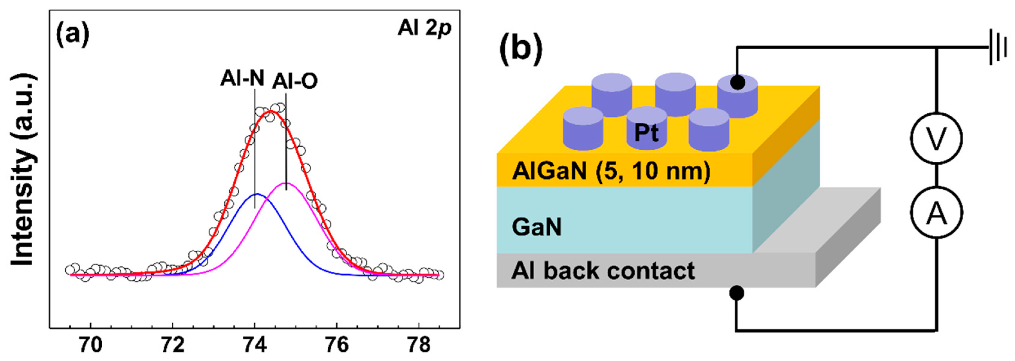
The ALD growth of AlGaN on c-plane (0001) GaN substrate was carried out using a thermal ALD system after native oxide removal process in an HCl:H2O (1:1) solution. Both 5 and 10 nm thick AlGaN layers were grown at 335 °C using trimethylaluminum (TMA), triethylgallium (TEG), and NH3 as Al, Ga, and N precursors, respectively. The ALD reaction was composed of TMA (TEG) feeding, N2 purge, NH3 feeding, and N2 purge. AlGaN growth was done by the combination of GaN and AlN reactions with a pulse ratio of 1:1, corresponding to Al0.85Ga0.15N. According to the X-ray photoelectron spectroscopy (XPS) analysis, we found that the dominant peak in the Al 2p core-level spectra shifted to lower binding energy with the increase of AlN thickness due to a strong Al–Al peak, which was associated with the strain relaxation generated from the lattice mismatch between AlN and GaN [16]. In other words, when the thickness of AlN exceeded ~10 nm, the strain relaxation affected the overgrown AlN film quality. Figure 1a shows the XPS core-level spectrum obtained from 10 nm thick AlGaN surface, revealing no clear evidence of the Al–Al peak. This indicates that the effect of strain relaxation is insignificant. In order to minimize the effect of strain relaxation, we prepared relatively thin AlGaN layers such as 5 and 10 nm in this work. In order to characterize the electrical properties, AlGaN/GaN Schottky diodes were fabricated with a 50 nm thick Pt front contact (diameter: 500 μm) and a 100 nm thick Al contact was deposited over the entire back surface. Figure 1b shows the schematic layer structures of the devices. Current–voltage (I–V) and capacitance–voltage (C–V) measurements were carried out with a Keithley 238 current source and an HP 4284A LCR meter, respectively.

Figure 1.
(a) X-ray photoelectron spectroscopy (XPS) Al 2p core-level spectrum obtained from 10 nm thick AlGaN surface and (b) schematic layer structures of the devices.
3. Results
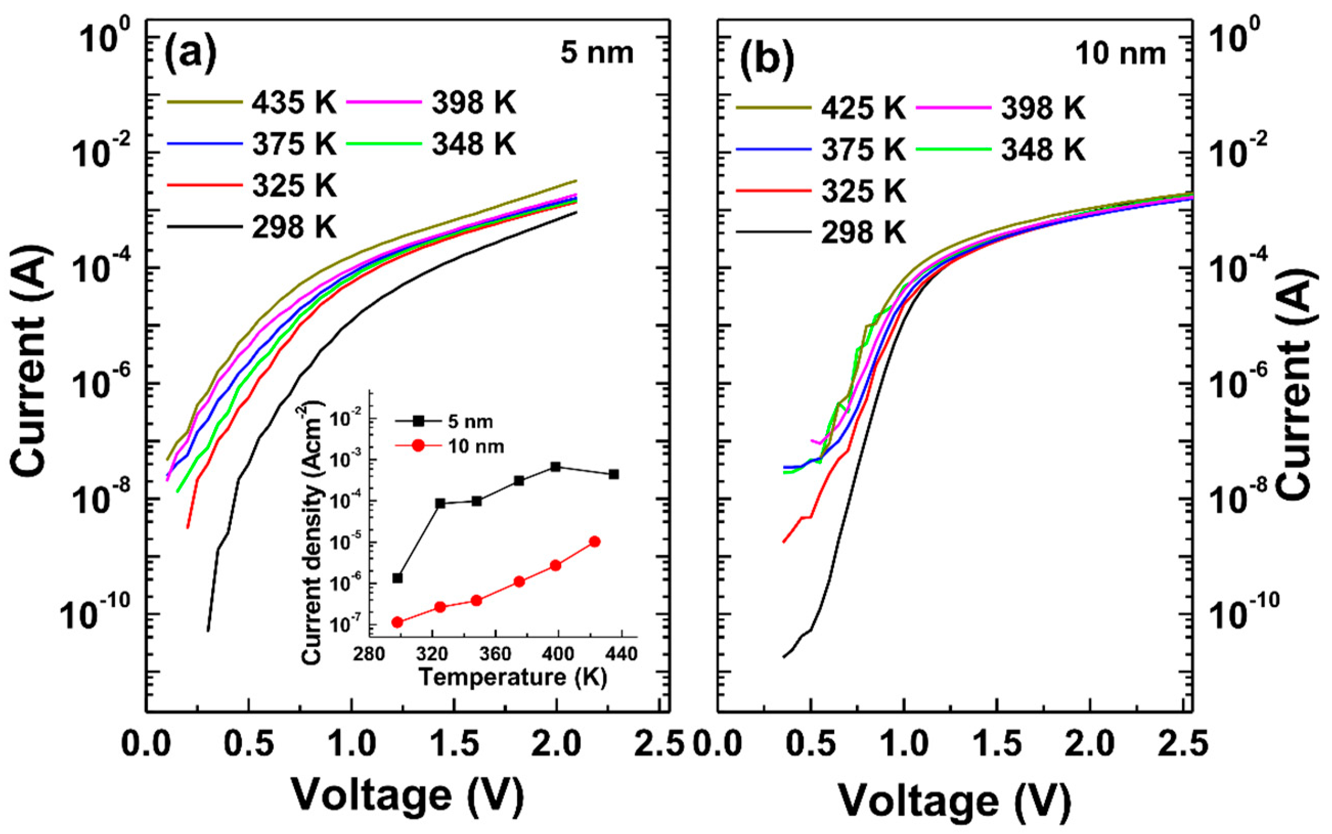
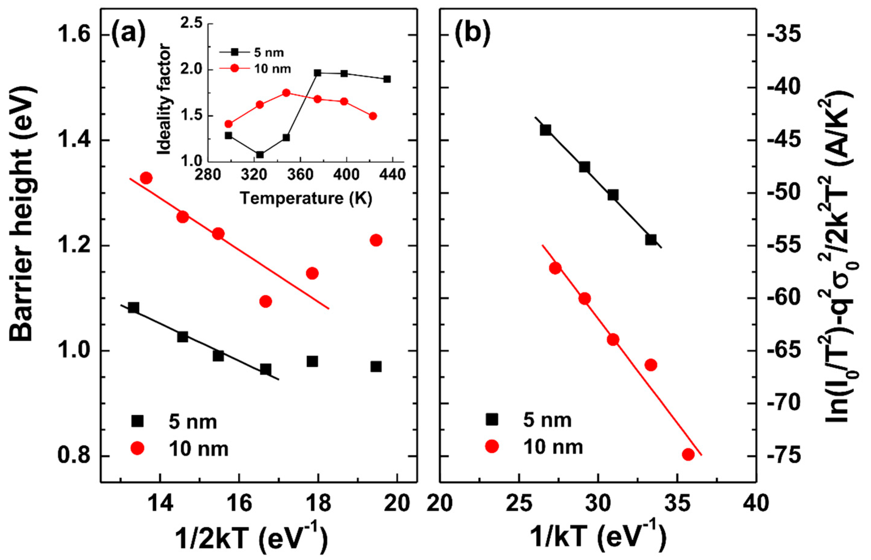
Figure 2 shows the forward I–V data obtained at various temperatures. Using the thermionic emission (TE) model [17], the barrier heights were calculated. Here, we calculated the theoretical effective Richardson constant using the equation, , where h is Plank’s constant and m* is the effective electron mass in AlGaN [18] and obtained the Richardson constant of Al0.85Ga0.15N as 40.0 Acm−2 K−2. The barrier height vs. temperature is described as , where is the zero-bias mean barrier height and is the standard deviation. The plots of vs. 1/2kT are shown in Figure 3a. The barrier heights for 10 nm thick AlGaN are higher than those for 5 nm thick AlGaN. The linear fits to plots of vs. 1/2kT were applied to the temperature ranges of 325–425 K and 348–435 K, respectively, for 5 and 10 nm thick AlGaN. The linear fits yielded the values of = 1.55 eV and = 0.19 V for 5 nm thick AlGaN and the values of = 1.98 eV and = 0.22 V for 10 nm thick AlGaN. The modified Richardson plot with the lateral barrier inhomogeneity considered is described as follows:
where I0 is the reverse bias saturation current and A is the Schottky contact area. Figure 3b shows plots of vs. 1/kT. The intercepts at the ordinate produced modified Richardson constants of 44.8 and 44.4 Acm−2 K−2, respectively, for 5 and 10 nm thick AlGaN. These values are similar to the theoretical value of 40.0 Acm−2K−2 for Al0.85Ga0.15N. Therefore, the forward current flows for AlGaN/GaN Schottky contacts can be explained by the TE model with Schottky barrier inhomogeneity.
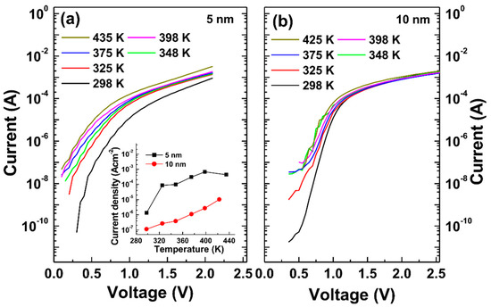
Figure 2.
Current–voltage (I–V) data obtained at various temperatures: (a) 5 nm and (b) 10 nm thick AlGaN samples. The inset in (a) shows the reverse leakage current densities at −10 V.
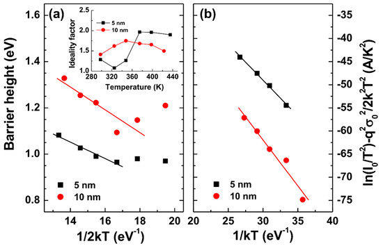
Figure 3.
(a) Barrier height vs. 1/2kT plots and (b) modified Richardson plots. The inset in (a) shows the ideality factors.
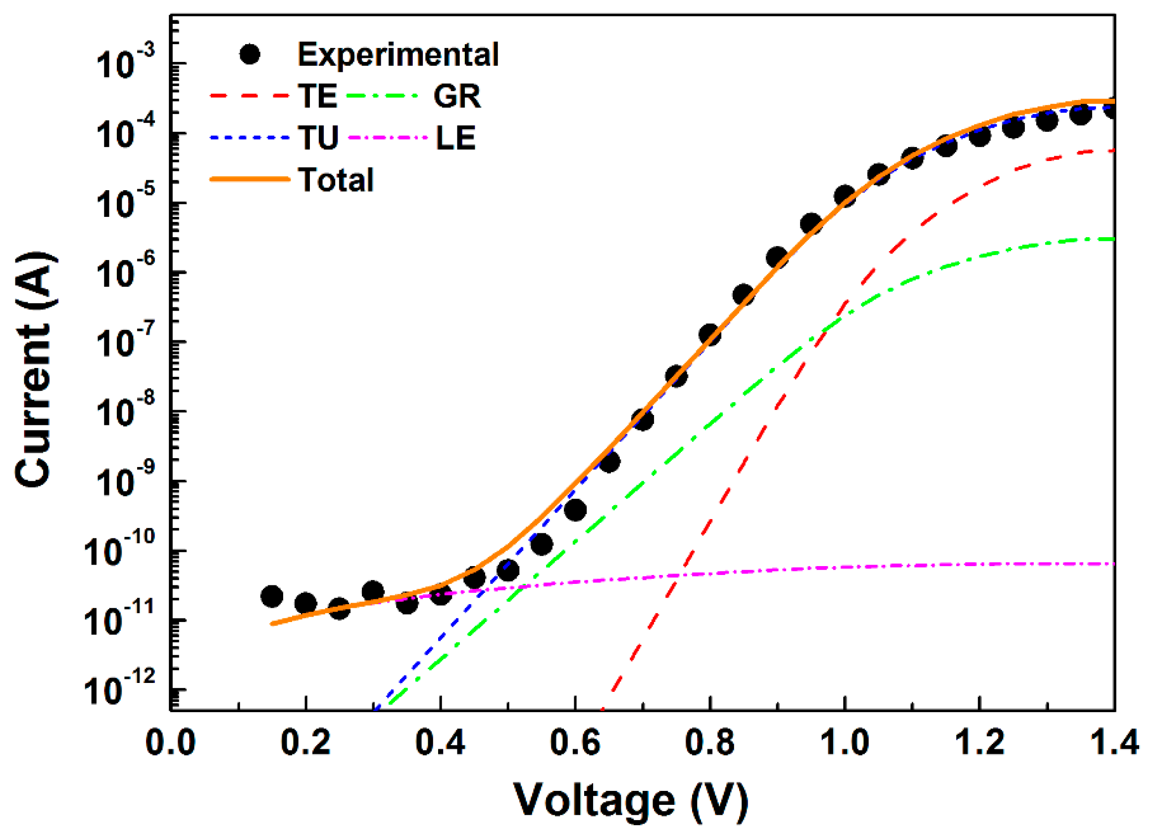
To clarify the current transport mechanism more thoroughly, other transport components were considered comprehensively. The total current ITOT, was assumed to be the combination of different transport mechanisms, given by [19]:
where ITE is the TE current, IGR is the generation-recombination (GR) current, ITU is the tunneling current (TU), and ILE is the leakage current. (ΦB: barrier height), , and are the saturation currents of TE, GR, and TU components, respectively. is a parameter, where is the tunneling characteristic energy. RS is the series resistance, which can be extracted from the curves where the I–V data begin to saturate and RSh is the shunt resistance. We fitted the experimental forward I–V curves to theoretical I–V data by taking , , , and E0 as fitting parameters. The experimental and fitted data at 298 K for 10 nm thick AlGaN are shown in Figure 4 as an example.
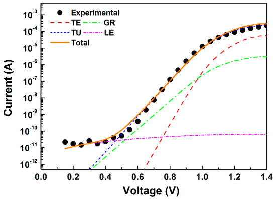
Figure 4.
The fitting results of the forward I–V data at 298 K for a 10 nm thick AlGaN sample are shown.
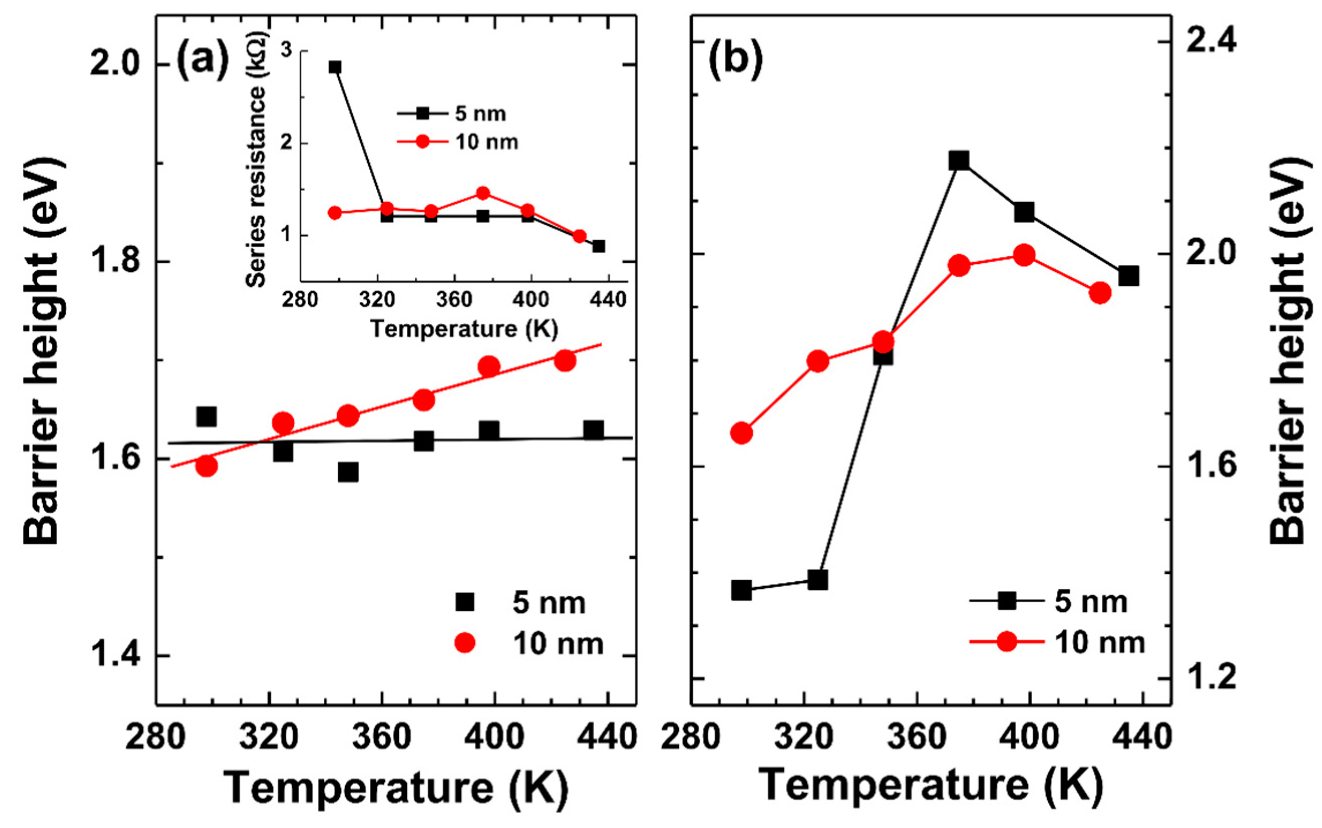
The barrier heights were calculated from values of the TE component at different temperatures, which are shown in Figure 5a. The barrier heights showed very little temperature dependence for 5 nm thick AlGaN, but these increased slightly with temperature for 10 nm thick AlGaN. The relation between barrier height and bandgap energy (Eg) is roughly approximated as [20]. The bandgap of Al0.85Ga0.15N was found to be about 5.65 eV based on the argument by Pelá et al. [21]. Then, the barrier height can be obtained as 1.88 eV. This value is higher than the values in Figure 5a but is closer to the zero-bias mean barrier height of 1.98 eV for 10 nm thick AlGaN. The flat-band barrier height was also determined using the barrier height and the ideality factor (n), which is given by [22]:
where NC is the density of states at the conduction band and ND is the carrier concentration. Under the flat-band condition, the electric field in the semiconductor is zero and the effects of image force lowering and tunneling on the I–V properties are negligible. Figure 5b shows the obtained flat-band barrier heights. At higher temperatures (above 348 K), the values for both samples are closer to the value of 1.88 eV.
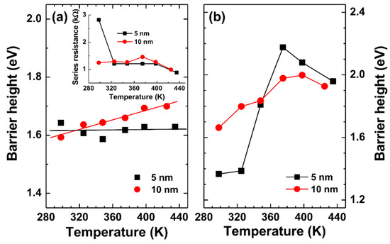
Figure 5.
(a) Barrier heights obtained from thermionic emission (TE) component and (b) flat-band barrier heights. The inset in (a) shows the series resistances obtained from the fitting.
According to the dislocation-governed tunneling current model, the tunneling saturation current at 0 K can be described as [20]:
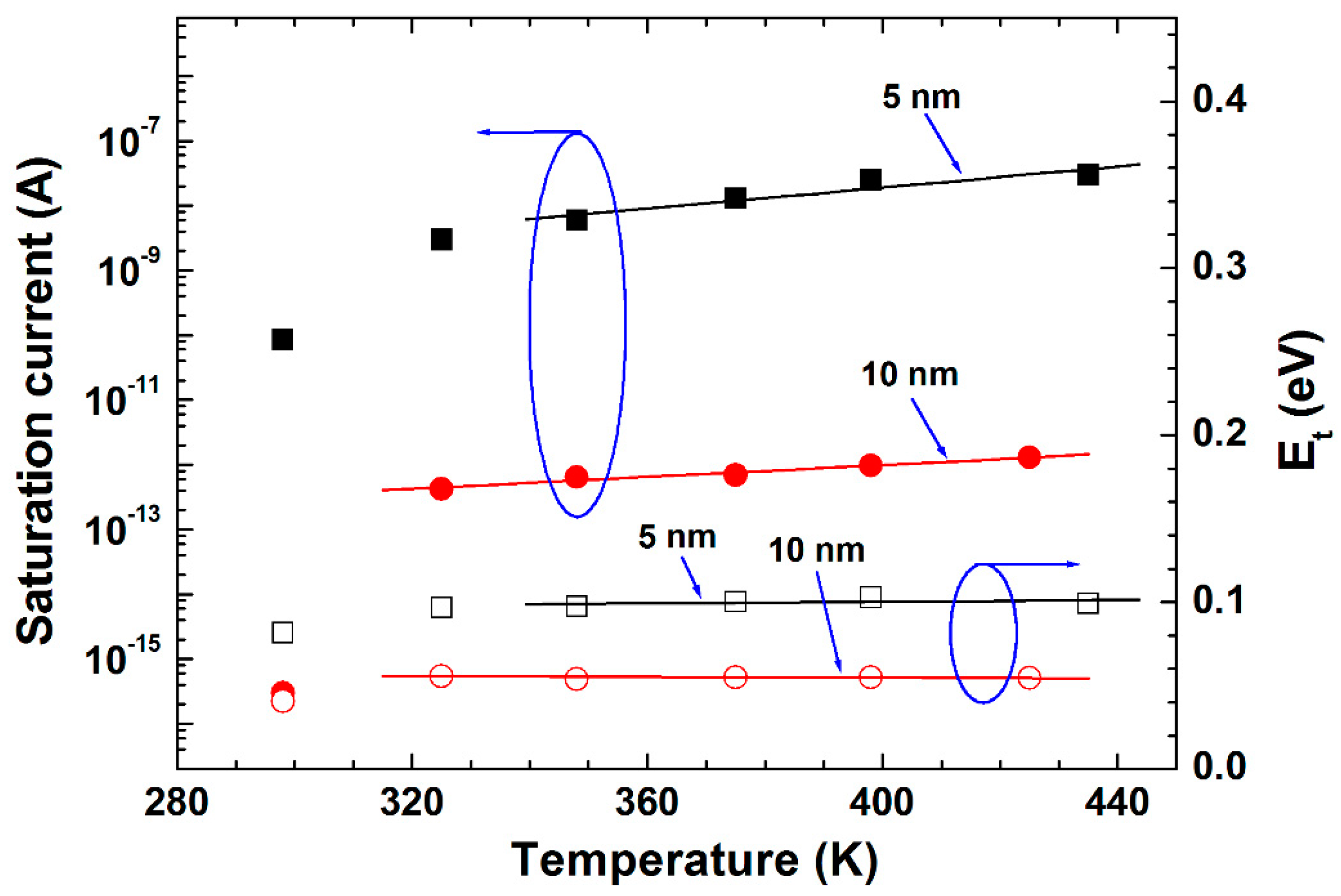
where vD (~1.5 × 10¹³ s−1 [23]) is the Debye frequency and Ndis is the dislocation density. Figure 6 shows the tunneling saturation current () and the barrier energy (Et). We extrapolated the linear fitting to the data in Figure 6 to attain and Et at 0 K. The barrier energy revealed a weak temperature dependence, indicating that the tunneling current is dominant. The tunneling saturation currents deviated from linearity at low temperatures and thus, some data were not included in the fitting. Finally, the dislocation densities were calculated to be 6.16 × 10⁵ and 1.38 × 1010 cm−2, respectively, for 5 and 10 nm thick AlGaN. Figure 7a shows the atomic force microscopy (AFM) surface image of 5 nm thick AlGaN measured over 1 μm × 1 μm scan area. The randomly distributed dark pits are observed over all the scan area. The small pits for GaN surface are known to represent the threading dislocations (TDs) with mixed and screw components where step edges meet, and pure edges meet when the components are on a terrace [24]. The values of TDs for Al0.7Ga0.3N grown by metalorganic chemical vapor deposition (MOCVD) were also obtained from AFM images, which were found to be 2.5 × 109 cm−2. [25]. In this regard, we assumed that the density of pits are comparable to the density of TDs. The densities of these pits were measured to be 5.8 × 1010 cm−2 for 5 nm thick AlGaN. As shown in Figure 7b the AFM image of 10 nm thick AlGaN does not reveal clearly distributed dark pits (though dark regions are observed). Even though we tried to obtain AFM images from different regions, we could not get an image similar to that of the 5 nm thick AlGaN. Nevertheless, it is possible to assume that the density of TDs would not decrease (or increase) significantly after increasing the AlGaN thickness from 5 to 10 nm. Both 5 and 10 nm thick AlGaN might have similar densities of TDs. Consequently, the density of TDs from AFM is similar to the value of 1.38 × 1010 cm−2 from 10 nm thick AlGaN but is much higher than that from 5 nm thick AlGaN. This implies that the dislocation-related tunneling current transport is the dominant mechanism in 10 nm thick AlGaN. However, such a mechanism cannot be applied to 5 nm thick AlGaN.
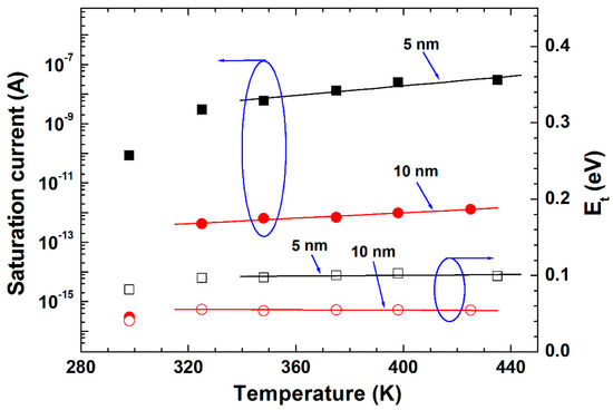
Figure 6.
Tunneling saturation current and barrier energy vs. temperature.
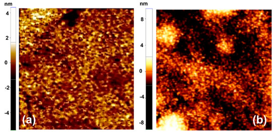
Figure 7.
Atomic force microscope (AFM) images of (a) 5 nm and (b) 10 nm thick AlGaN surface scanned over 1 μm × 1 μm.
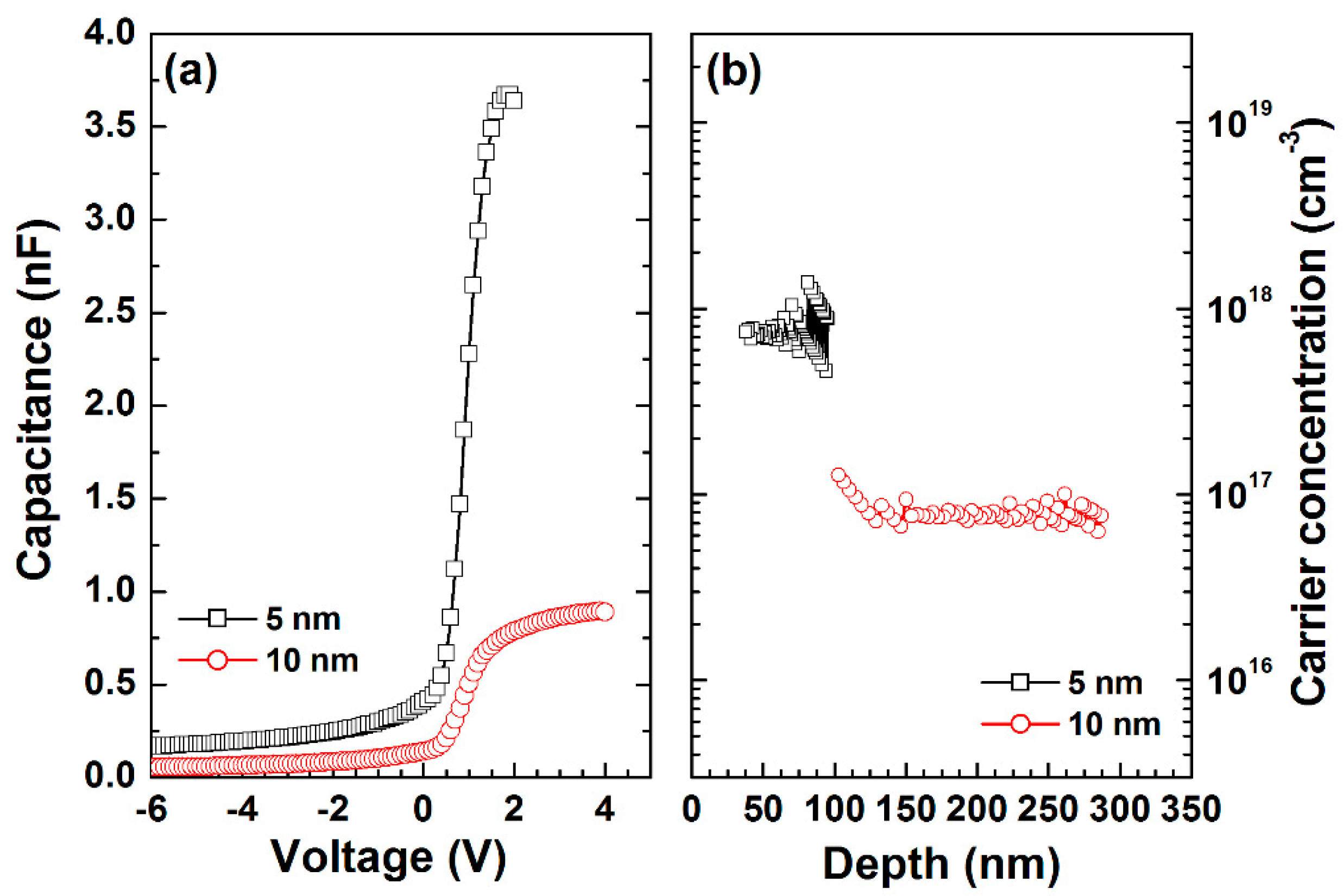
Figure 8a shows the C–V data measured at room temperature. Here, C–V characterization was performed at a frequency of 100 kHz to reduce the measurement error arising from the series resistance. The carrier concentration vs. depth was obtained, as shown in Figure 8b. The carrier concentration of ~8 × 1016 cm−3 was obtained for 10 nm thick AlGaN, similar to the value provided by the vendor. However, 5 nm thick AlGaN was found to have a much higher value of ~8 × 1017 cm−3. For n-type semiconductors, the Schottky barrier height is:
with , where = 5.65 eV is the work function of Pt [26], is the surface work function of AlGaN, χ is the electron affinity of AlGaN, and qVS is the surface band bending energy. By assuming that the electron affinity vs. x in AlxGa1−xN (χGaN = 4.2 eV and χAlN = 2.05 eV) varies linearly [18], we obtained χ = 2.37 eV for Al0.85Ga0.15N. Then, the barrier height can be written as:
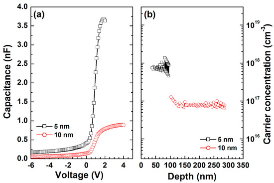
Figure 8.
(a) Capacitance–voltage (C–V) characteristics measured at 100 kHz and (b) carrier concentration profiles vs. depth.
By using the barrier heights from C–V measurements, the surface state density (NS) was calculated through the following equation [27]:
where ε is the dielectric constant of AlGaN. The surface state densities at AlGaN surface were found to be 3.9 × 10¹² and 1.1 × 1012 cm−2, respectively, for 5 and 10 nm thick AlGaN. This clearly indicates the higher surface state density for 5 nm thick AlGaN. According to the thin surface barrier (TSB) model, the presence of surface donors can reduce the barrier width so that electrons tunnel through the thinner potential barrier easily [8,28]. Nitrogen vacancies and oxygen impurities in AlGaN may be the origin of surface donors [29,30].
Because the interface states of a Schottky diode at the metal/semiconductor interface cannot follow the high-frequency signal, they do not contribute to the capacitance at high frequencies. Hence, the measured capacitance at a high-frequency consists of space–charge capacitance (). At low-frequencies, the total capacitance consists of the space–charge capacitance () and the interface capacitance (), which can be described as [31]. The interface state density () can be written as [32]:
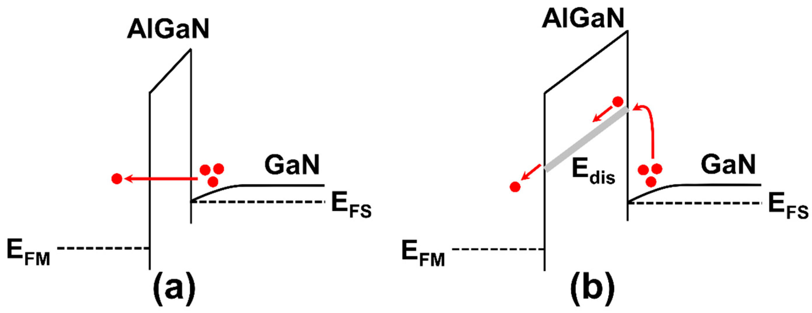
The interface state energy () below the conduction band () at the semiconductor surface is given by [31,32]. The high and low-frequency C–V characteristics were obtained at 500 and 1 kHz, respectively. Using Equation (12), the interface state density was calculated over the depletion region. Here, we conjecture that both the energy states at the AlGaN/GaN interface and near the AlGaN surface might contribute to the interface state density. As shown in Figure 9, the interface state density for 5 nm thick AlGaN was found to be higher. As a result, higher interface state density and a thinner AlGaN barrier layer might enhance the tunneling current for 5 nm thick AlGaN (i.e., direct tunneling could occur significantly) while the tunneling current is related to the TDs for 10 nm thick AlGaN (i.e., trap assisted tunneling might occur through TDs). Figure 10 shows the schematic band structures for each sample describing the dominant current transport mechanism.
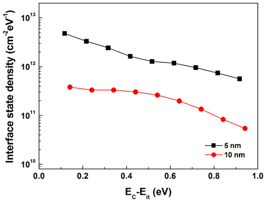
Figure 9.
The energy distribution curves of the interface states obtained from the high- and low-frequency C–V characteristics.
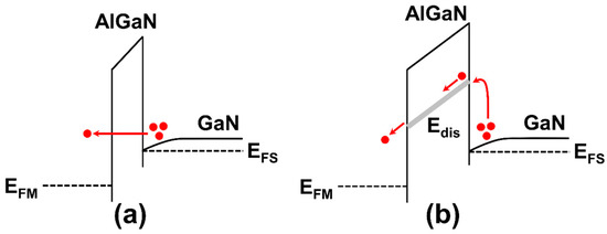
Figure 10.
Schematic band diagrams presenting the dominant current transport under forward bias conditions for (a) 5 and (b) 10 nm thick AlGaN.
As shown in Figure 8a, both samples show that the transition from depletion to accumulation occurred above 0 V, indicating that negative charges are present in the AlGaN layer. Normally AlGaN/GaN Schottky diodes and HEMTs have the transition voltages as negative values [11,33]. Systematic investigation of thermal annealing on AlGaN/GaN HEMTs with different fluorine plasma treatment revealed the positive shift in the C–V characteristics with the increasing of the plasma power, which negatively shifted after thermal annealing [34]. It was explained by the fact that F– ions introduced the acceptor-like states in the AlGaN barrier layer and subsequent annealing eliminated some plasma-induced trap states. When acceptor-like defects are present, C–V curves stretch out in a positive direction [35]. Oxygen plasma treatment on AlGaN/GaN HEMTs was found to cause a positive shift, reducing the content of the Al component in the AlGaN barrier layer and depleting channel electrons [36]. The mechanism for positive flatband voltage shift and the depletion of electron gas due to oxygen plasma treatment was explained by gradual conversion of the AlGaN barrier layer into an AlON/GaON structure [36]. The acceptor-like traps were associated with the oxidation of the recessed AlGaN surface during ALD growth [12]. Analysis on the X-ray photoelectron spectroscopy for 10 nm thick AlGaN (not shown) showed that the atomic percentage of oxygen atoms was about 15% in the AlGaN layer, indicating that the AlGaN layer is highly oxidized. Furthermore, 2DEG density according to the method by Lv et al. [37] was calculated to be about 1.1 × 1012 cm2 for both samples. This is too low compared to other works [37,38]. During the ALD growth, many acceptor-like defects might be formed in the AlGaN layer and then, the electrons from the surface donors were captured while moving from the AlGaN surface to the AlGaN/GaN interface, lowering the 2DEG density and forming the negative charges. Based on the study using post metallization annealing, it was proposed that the charges caused by interfacial defects could be passivated and neutralized through an H2-based annealing [39]. Thus, thermal annealing on ALD-AlGaN will be necessary to improve the interfacial quality of AlGaN/GaN structure.
4. Conclusions
We characterized the current transport properties of AlGaN/GaN Schottky diodes with an ALD-grown AlGaN layer. At higher temperatures (above 348 K), both 5 and 10 nm thick AlGaN showed that the TE model with Schottky barrier inhomogeneity was appropriate to explain the current flow. Higher barrier height for 10 nm thick AlGaN was obtained compared to 5 nm thick AlGaN. We fitted the experimental I–V data to the theoretical values with the consideration of various transport mechanisms. The dislocation-governed tunneling model was matched well to the experimental data for 10 nm thick AlGaN, however, it was not applicable to 5 nm thick AlGaN. A higher density of surface (and interface) states was found for 5 nm thick AlGaN, leading to a thinner tunneling barrier. Direct tunneling might occur significantly for 5 nm thick AlGaN while TD-related trap assisted tunneling was dominant for 10 nm thick AlGaN. Reducing the density of acceptor-like defects and minimizing the incorporation of oxygen atoms in AlGaN is highly required during the ALD growth. Even though the diode characteristics are not sufficiently good, the results obtained from this work will be meaningful for the understanding of the properties of ALD-AlGaN, in terms of both devices and materials. For example, the ALD growth can be applied to nanostructured layers with uniform thickness. In such nanoscale devices, the information obtained from the ALD-AlGaN layer is helpful in understanding device performance.
Author Contributions
Conceptualization, H.K.; methodology, H.K. and B.J.C.; investigation, H.K. and S.C.; writing—original draft, H.K.; writing—review and editing, H.K. and B.J.C. All authors have read and agreed to the published version of the manuscript.
Funding
This work was supported by the Basic Science Research Program through the National Research Foundation of Korea (NRF) funded by the Ministry of Education (2017R1D1A1B03030400).
Conflicts of Interest
The authors declare no conflict of interest.
References
- Ibbetson, J.; Fini, P.; Ness, K.; DenBaars, S.; Speck, J.; Mishra, U. Polarization effects, surface states, and the source of electrons in AlGaN/GaN heterostructure field effect transistors. Appl. Phys. Lett. 2000, 77, 250–252. [Google Scholar] [CrossRef]
- Ambacher, O.; Smart, J.; Shealy, J.; Weimann, N.; Chu, K.; Murphy, M.; Schaff1, W.; Eastman, L.; Dimitrov, R.; Wittmer, L.; et al. Two-dimensional electron gases induced by spontaneous and piezoelectric polarization charges in N- and Ga-face AlGaN/GaN heterostructures. J. Appl. Phys. 1999, 85, 3222–3233. [Google Scholar] [CrossRef]
- Ambacher, O.; Majewski, J.; Miskys, C.; Link, A.; Hermann, M.; Eickhoff, M.; Stutzmann, M.; Bernardini, F.; Fiorentini, V.; Tilak, V.; et al. Pyroelectric properties of Al(In)GaN/GaN hetero- and quantum well structures. J. Phys. Condens. Matter. 2002, 14, 3399–3434. [Google Scholar] [CrossRef]
- Marcon, D.; Viaene, J.; Favia, P.; Bender, H.; Kang, X.; Lenci, S.; Decoutere, S. Reliability of AlGaN/GaN HEMTs: Permanent leakage current increase and output current drop. Microelectron. Reliab. 2012, 52, 2188–2193. [Google Scholar] [CrossRef]
- Usami, S.; Ando, Y.; Tanaka, A.; Nagamatsu, K.; Deki, M.; Kushimoto, M.; Nitta, S.; Honda, Y.; Amano, H.; Sugawara, Y.; et al. Correlation between dislocations and leakage current of p-n diodes on a free-standing GaN substrate. Appl. Phys. Lett. 2018, 112, 182106. [Google Scholar] [CrossRef]
- Simpkins, B.; Yu, E.; Waltereit, P.; Speck, J. Correlated scanning Kelvin probe and conductive atomic force microscopy studies of dislocations in gallium nitride. J. Appl. Phys. 2003, 94, 1448–1453. [Google Scholar] [CrossRef]
- Besendörfer, S.; Meissner, E.; Lesnik, A.; Friedrich, J.; Dadgar, A.; Erlbacher, T. Methodology for the investigation of threading dislocations as a source of vertical leakage in AlGaN/GaN-HEMT heterostructures for power devices. J. Appl. Phys. 2019, 125, 095704. [Google Scholar] [CrossRef]
- Hashizume, T.; Kotani, J.; Hasegawa, H. Leakage mechanism in GaN and AlGaN Schottky interfaces. Appl. Phys. Lett. 2004, 84, 4884–4886. [Google Scholar] [CrossRef]
- Yan, D.; Lu, H.; Cao, D.; Chen, D.; Zhang, R.; Zheng, Y. On the reverse gate leakage current of AlGaN/GaN high electron mobility transistors. Appl. Phys. Lett. 2010, 97, 153503. [Google Scholar] [CrossRef]
- Ha, W.; Chhajed, S.; Oh, S.; Hwang, S.; Kim, J.; Lee, J.; Kim, K. Analysis of the reverse leakage current in AlGaN/GaN Schottky barrier diodes treated with fluorine plasma. Appl. Phys. Lett. 2012, 100, 132104. [Google Scholar]
- Ren, J.; Yan, D.; Zhai, Y.; Mou, W.; Gu, X. Comparison of electrical characteristics between AlGaN/GaN and lattice-matched InAlN/GaN heterostructure Schottky barrier diodes. Microelctron. Rel. 2016, 61, 82–86. [Google Scholar] [CrossRef]
- Huang, S.; Liu, X.; Wei, K.; Liu, G.; Wang, X.; Sun, B.; Yang, X.; Shen, B.; Liu, C.; Liu, S.; et al. O3-sourced atomic layer deposition of high quality Al2O3 gate dielectric for normally-off GaN metal-insulator-semiconductor high electron-mobility transistors. Appl. Phys. Lett. 2015, 106, 033507. [Google Scholar] [CrossRef]
- George, S. Atomic layer deposition: An overview. Chem. Rev. 2010, 110, 111–131. [Google Scholar] [CrossRef]
- Ozgit, C.; Donmez, I.; Alevli, M.; Biyikli, N. Atomic layer deposition of GaN at low temperatures. J. Vac. Sci. Technol. A 2013, 30, 01A124. [Google Scholar] [CrossRef]
- Ozgit-Akgun, C.; Goldenberg, E.; Okyay, A.; Biyikli, N. Hollow cathode plasma-assisted atomic layer deposition of crystalline AlN, GaN and AlxGa1−xN thin films at low temperatures. J. Mater. Chem. C 2014, 2, 2123–2236. [Google Scholar] [CrossRef]
- Kim, H.; Kim, N.; An, S.; Yoon, H.; Choi, B. Improved interfacial properties of thermal atomic layer deposited AlN on GaN. Vacuum 2019, 159, 379–381. [Google Scholar] [CrossRef]
- Tung, R. Recent advances in Schottky barrier concepts. Mater. Sci. Eng. R. 2001, 35, 1–138. [Google Scholar] [CrossRef]
- Qiao, D.; Yu, L.; Lau, S.; Redwing, J.; Lin, J.; Jiang, H. Dependence of Ni/AlGaN Schottky barrier height on Al mole fraction. J. Appl. Phys. 2000, 87, 801–804. [Google Scholar] [CrossRef]
- Suzue, K.; Mohammad, S.; Fan, Z.; Kim, W.; Aktas, O.; Botchkarev, A.; Morkoç, H. Electrical conduction in platinum–gallium nitride Schottky diodes. J. Appl. Phys. 1996, 80, 4467–4478. [Google Scholar] [CrossRef]
- Donoval, D.; Chvála, A.; Šramatý, R.; Kováč, J.; Morvan, E.; Dua, C.; DiForte-Poisson, M.; Kordoš, P. Transport properties and barrier height evaluation in Ni/InAlN/GaN Schottky diodes. J. Appl. Phys. 2011, 109, 063711. [Google Scholar] [CrossRef]
- Pelá, R.; Caetano, C.; Marques, M.; Ferreira, L.; Furthmüller, J.; Teles, L. Accurate band gaps of AlGaN, InGaN, and AlInN alloys calculations based on LDA-1/2 approach. Appl. Phys. Lett. 2011, 98, 151907. [Google Scholar] [CrossRef]
- Wagner, A.; Young, W.; Sugerman, A. A note on the correlation between the Schottky-diode barrier height and the ideality factor as determined from I-V measurements. IEEE Electron Device Lett. 1983, 4, 320–322. [Google Scholar] [CrossRef]
- Belyaev, A.; Boltovets, N.; Ivanov, V.; Klad’ko, V.; Konakova, R.; Kudrik, Y.; Kuchuk, A.; Milenin, V.; Sveshnikov, Y.; Sheremet, V. Mechanism of dislocation-governed charge transport in Schottky diodes based on gallium nitride. Semiconductors 2008, 42, 689–693. [Google Scholar] [CrossRef]
- Tarsa, E.; Heying, B.; Wu, X.; Fini, P.; DenBarrs, S.; Speck, J. Homoepitaxial growth of GaN under Ga-stable and N-stable conditions by plasma-assisted molecular beam epitaxy. J. Appl. Phys. 1997, 82, 5472–5479. [Google Scholar] [CrossRef]
- Moseley, M.; Allerman, A.; Crawford, M.; Wierer, J., Jr.; Smith, M.; Biedermann, L. Electrical current leakage and open-core threading dislocations in AlGaN-based deep ultraviolet light-emitting diodes. J. Appl. Phys. 2014, 116, 053104. [Google Scholar] [CrossRef]
- Michaelson, H. The work function of the elements and its periodicity. J. Appl. Phys. 1977, 48, 4729–4733. [Google Scholar] [CrossRef]
- Lee, C.; Lin, Y.; Liu, D. Schottky barrier height and surface state density of Ni/Au contacts to (NH4)2Sx–treated n-type GaN. Appl. Phys. Lett. 2001, 79, 2573–2575. [Google Scholar] [CrossRef]
- Hasegawa, H.; Susumu, O. Mechanism of anomalous current transport in n-type GaN Schottky contacts. J. Vac. Sci. Technol. B. 2002, 20, 1647–1655. [Google Scholar] [CrossRef]
- Gordon, L.; Miao, M.; Chowdhury, S.; Higashiwaki, M.; Mishra, U.; Walle, C. Distributed surface donor states and the two-dimensional electron gas at AlGaN/GaN heterojunctions. J. Phys. D Appl. Phys. 2010, 43, 505501. [Google Scholar] [CrossRef]
- Hashizume, Y.; Kotani, J.; Basile, A.; Kaneko, M. Surface control process of AlGaN for suppression of gate leakage currents in AlGaN/GaN heterostructure field effect transistors. Jpn. J. Appl. Phys. 2006, 45, L111–L113. [Google Scholar] [CrossRef]
- Özdemir, A.; Türüt, A.; Kökce, A. The interface state energy distribution from capacitance–frequency characteristics of gold/n-type Gallium arsenide Schottky barrier diodes exposed to air. Thin Solid Films 2003, 425, 2010–2015. [Google Scholar] [CrossRef]
- Lee, C.; Lin, C.; Lee, H.; Chen, P. Changes in surface state density due to chlorine treatment in GaN Schottky ultraviolet photodetectors. J. Appl. Phys. 2008, 103, 094504. [Google Scholar] [CrossRef]
- Enisherlova, K.; Goryachev, V.; Rusak, T.; Kapilin, S. Study of the effect of passivation layers on capacitance of AlGaN/GaN heterostructures. Modern Electron. Mater. 2016, 2, 131–137. [Google Scholar] [CrossRef]
- He, Y.; Mi, M.; Zhang, M.; Wang, C.; Ma, X.; Hao, Y. Influence of Thermal Annealing on AlGaN/GaN HEMT by Fluorine Plasma Treatment. In Proceedings of the 2016 13th China International Forum on Solid State Lighting: International Forum on Wide Bandgap Semiconductors China (SSLChina: IFWS), Beijing, China, 15–17 November 2016; IEEE: Piscataway, NJ, USA, 2016; pp. 116–119. [Google Scholar]
- Miczek, M.; Mizue, C.; Hashizume, T.; Adamowicz, B. Effects of interface states and temperature on the C–V behavior of metal/insulator/AlGaN/GaN heterostructure capacitors. J. Appl. Phys. 2008, 103, 104510. [Google Scholar] [CrossRef]
- He, Y.; Wang, C.; Mi, M.; Zheng, X.; Zhang, M.; Zhao, M.; Zhang, H.; Chen, L.; Zhang, J.; Ma, Z.; et al. Recessed-gate quasi-enhancement-mode AlGaN/GaN high electron mobility transistors with oxygen plasma treatment. Chin. Phys. B. 2016, 25, 117305. [Google Scholar] [CrossRef]
- Zhang, K.; Chen, X.; Mi, M.; Zhao, S.; Chen, Y.; Zhang, J.; Ma, X.; Hao, Y. Enhancement-mode AlGaN/GaN HEMTs with thin and high Al composition barrier layers using O2 plasma implantation. Phys. Status Solidi A. 2015, 212, 1081–1085. [Google Scholar] [CrossRef]
- Lv, Y.; Lin, Z.; Corrigan, T.; Zhao, J.; Cao, Z.; Meng, L.; Luan, C.; Wang, Z.; Chen, H. Extraction of AlGaN/GaN heterostructure Schottky diode barrier heights from forward current-voltage characteristics. J. Appl. Phys. 2011, 109, 074512. [Google Scholar] [CrossRef]
- Hung, T.; Krishnamoorthy, S.; Esposto, M.; Nath, D.; Park, P.; Rajan, S. Interface charge engineering at atomic layer deposited dielectric/III-nitride interfaces. Appl. Phys. Lett. 2013, 102, 072105. [Google Scholar] [CrossRef]
© 2020 by the authors. Licensee MDPI, Basel, Switzerland. This article is an open access article distributed under the terms and conditions of the Creative Commons Attribution (CC BY) license (http://creativecommons.org/licenses/by/4.0/).

