Article

Anomalous Heat Transport in Nanolaminate Metal/Oxide Multilayer Coatings: Plasmon and Phonon Excitations

1
Surface Phenomena Researches Group, I.P. Bardin Central Research Institute for Ferrous Metallurgy, 105005 Moscow, Russia
2
Instituto de Ciencia de Materiales de Madrid, Consejo Superior de Investigaciones Científicas, E-28049 Madrid, Spain
3
Basque Center for Materials, Applications & Nanostructures, UPV/EHU Science Park, Barrio Sarriena s/n, 48940 Leioa, Spain
4
IKERBASQUE, Basque Foundation for Science, Maria Diaz de Haro 3, 48013 Bilbao, Spain
*
Author to whom correspondence should be addressed.
Coatings 2020, 10(3), 260; https://doi.org/10.3390/coatings10030260
Submission received: 27 January 2020 / Revised: 9 March 2020 / Accepted: 10 March 2020 / Published: 11 March 2020
(This article belongs to the Special Issue Nanolaminate Multilayer Coatings)

Abstract

:
In this work, the anomalous reduction in the thermal conduction observed for nanolaminate metal-dielectric multilayers has been extended to the case of oxides. For this purpose, Ag/Al2O3 coatings were produced with different layer thicknesses (from 1 to 5 nm for Ag and 8 to 40 nm for Al2O3) and numbers of stacks. It was found that the thermal conduction is significantly lower in such metal–oxide nanolaminates compared to the bulk oxide. Such anomalous behaviour is explained by the influence of plasmon and phonon propagation confinement in nanolayers and at the interfaces. To this end, the characteristics of the different types of acoustic and optical phonon waves propagating in the multilayer coating have been studied. In particular, the electronic structures of the different layers and their influences on the plasmon resonance are investigated as a function of the multilayer design. The plasmon-polariton mechanism of energy transfer through oxide–metal and metal–oxide interfaces is discussed.

Graphical Abstract

1. Introduction

Presently, it is well known that miniaturization to the nanoscale in multilayer coatings (planar metamaterials) allows one to change, sharply, many of their physical properties, including electronic and optical ones. Such responses result from strong transformations in the electronic structures of the nanoscale materials, which, for example, can be reflected in shift of the binding energies of core-levels as measured by X-ray photoelectron spectroscopy (XPS) [1] or the frequency shifts of Raman modes in the so called “optical mode softening” and “acoustic mode hardening” [2]. Special attention should be paid to metal–insulator–metal (MIM) multilayer coatings that can be considered as the new class of planar metamaterials [3]. Electronic or atomic oscillations in MIM composites can transfer or transduce external electromagnetic radiation overrunning sub-diffraction limits [4]. Spatial localization of these wave processes, electron–phonon coupling and scattering directly influence the absorption and emission of electromagnetic waves in lot of optoelectronic devices and device transport dynamics [5]. Predicted specific optical or electromagnetic properties of such metamaterials are based on anomalies of phonons and plasmon propagation in nanostructures [6] that also control the heat conductivities of the materials [7,8,9,10,11]. Therefore, there are good prospects to get multifunctional coatings with favourable combination of strength, optical, and heat protecting properties. Many theoretical studies address them through use in thermoelectric systems [12,13], optics and radiophysics [14], or optoelectronics [3,15,16]. The combination of specific optical and heat protecting properties is required for microlasers, whose power is limited by the heat damage of mirrors [17]. Another potential application of such MIM coatings could be protection of solar cells, including ones operating at high IR intensity [18], but the understanding of heat transfer mechanisms in such systems is still unclear.
The physical nature of heat transmission and scattering in multilayer systems has been well described by the models presented in [8,10,18,19] but the problem consists of inadequate extrapolation of these methods to nanomaterials taking into account the complicated evolution of their properties in the size range from hundreds down to a few nanometres. It was shown that surface states and quantum phenomena control the electronic structures of nanomaterials differently. The first ones prevail for relatively large dimensions, while the second ones are strongly variable with the nanomaterials’ electronic structures below several tens of nanometres. This was clearly demonstrated from size shifts of XPS lines in nanomaterials with various compositions and morphologies [20,21,22,23,24]. It is very hard to imagine the generalized response of surface states and quantum phenomena on the actuation of electronic and lattice subsystems by external electromagnetic waves, and this is even more complicated for MIM planar metamaterials. At the same time, there are data on the strong influence of the quantum effects on plasmon and phonon oscillations’ propagation in multilayer MIM coatings [25,26,27]. Hence, the question of interconnections between the heat conductivities of nanomaterials and their surface and quantum states is still not solved. Previously, we addressed said question in multilayer coatings with metal/nitride layers [25,26,27]. In this case, Ag was used as metal and a wurzite TiAlN layer [27] was used as dielectric media. In the present case, we extend our studies to oxide layers by using Al2O3 as the dielectric (insulating) layer. In particular, we address size effects (i.e., layer thickness) in the propagation of plasmons and phonons as heat carriers controlling the mechanisms of heat conductivity.

2. Materials and Methods

The set of multilayer Al2O3/Ag coatings was fabricated by DC–magnetron sputtering. The thicknesses of individual layers were varied from a few to several hundreds of nanometres. All the samples were covered with a protective top-most 200 nm Al2O3 layer to avoid silver oxidation before performing the electron spectroscopy experiments. Table 1 contains parameters of coatings that were used to investigate the difference between multilayer and monolithic coatings.
The layer structure of the coatings was verified by Rutherford backscattering spectrometry (RBS). The measurements were performed with the 5 MV Cockroft–Walton tandetron at the Centro de Microanálisis de Materiales (CMAM) in Madrid (Spain) using a 2 MeV He+ probing beam, and the backscattered ions were detected with a silicon detector at a scattering angle of 170°. The experimental RBS spectra were compared with simulated ones obtained from the SIMNRA code [28] assuming the corresponding sample layer structure.
The electron spectroscopy investigations were performed using the multifunctional electron spectrometer ESCALAB MK2 (VG, East Grinstead, UK) equipped by a monochromatic Al Kα X-ray source ( = 1486.6 eV), a scanning electron gun LEG200, and an EMU-50 source of monochromatic electrons (E0 = 1–100 eV). Carbon 1’s photoelectron peak with binding energy 285.0 eV was used as an internal reference to determine precisely the energy positions of other spectral lines. Prior to the analysis, the samples were sputter cleaned using Ar+ ions in the preparation chamber of the spectrometer at a pressure of 10−5 Pa, an accelerating voltage of 5 kV, and a current of 20 µA. The precise control over the lateral Ar+ ion etching profile attained with the AG-6 ion gun was used to fabricate 0.25° angle laps. Additionally, ion etching with simultaneous sample rotation was used for homogeneous thinning the Al2O3 blanket from 200 nm to 10 nm, its subsequent removal, and for uniform thinning of Ag layers. The parameters of spectra acquisition were selected to provide high energy spectral resolution with a full width at half maximum (FWHM) about 20 meV for high resolution electron energy loss spectroscopy (HREELS) investigations. Auger electron microscopy (AEM) and electron microscopy of characteristic losses were applied for imaging of the elemental mapping and plasmon intensity distribution through the small-angle cross-section of the multilayer coatings in both individual layers and at interfaces with primary electron energies, E0, of 1371.4 and 1401.5 eV. The resolution of images was 256 × 256 pixels at 10,000× magnification. The topographic contrast was suppressed by image acquisition software.
Thermal conductivity of the as-deposited coatings was measured by a pulsed photothermal reflectance (PPR) technique described in detail in [29].

3. Results and Discussion

3.1. Fundamentals of Thermal Transport in Metals and Dielectrics

The thermal conductivity of the Al2O3/Ag multilayer coating can be described by a two-phase system (1 = Ag, 2 = Al2O3) consisting of two repetitive nanolayers with thicknesses L1 and L2, thermal conductivities K1 and K2, and thermal resistance of a boundary between layers Rb. Therefore, the generalized thermal conductivity coefficient Kml of the multilayer coating with N bilayers can be described phenomenologically as [30]:
K ml = N ( L 1 + L 2 ) R ml = N ( L 1 + L 2 ) ( L 1 K 1 + L 2 K 2 ) + ( N 1 ) R b
According to Equation (1), the thermal conductivity decreases as the layers become thinner due to growing influence of interfaces. One shall take into account that thermal conductivities of nanolayers also decrease with thinning comparing to “bulk” reference values. Moreover, the thermal conductivity of metals is the sum of lattice (l) and electron (e) contributions:
K1 = Ke + Kl
However, these contributions are interrelated and also depend on the solid temperature. The phonon contribution in thermal conductivity is 10 times lower than the electronic one for Ag thin films [31].
The ability of electrons to transport heat, for instance, is hindered if they keep bumping into phonons (the vibrating lattice). For this reason, metals have a higher electrical resistivity at higher temperatures. In fact, the heat transport in a pure metal is mostly due to electron–phonon interactions that disrupt the momentum of conducting electrons. Non-metals tend to have a lower thermal conductivity, unless their phonons can carry heat efficiently, and, in essence, have no free electrons. In dielectrics with a low density of free electrons, the electronic conduction heat transfer mechanism could be discarded. The phonons part of thermal conductivity consist of three components:
Kl = KL + Kt0 + Ktu
where KL is the longitudinal phonon contribution (acoustic phonons), whereas Kt and Ktu are the contributions of low and high frequency transverse phonons, respectively. Acoustic oscillations play a major role in heat transfer by phonons. An important attribute of heat transfer is the phonon wavelength, because phonon propagation in the media and through the interphase boundaries is a wave process. For example, when the phonon mean free path becomes comparable to the layer thickness in the multilayer coating, the heat propagation perpendicular to interfaces is weakened due to nanoscale effects, as assessed in the thermal transportation of various dielectric materials [32]. Here, the authors introduce the concept of critical acoustic thickness of a film blocking heat transfer by phonons.
Electronic heat transport is the prevailing mechanism in metals, and it is controlled by electronic structure. According to our previous studies [1,20,21,22,23,24], it is drastically rearranged on the nanoscale. These theoretical views are the basis of the present research.

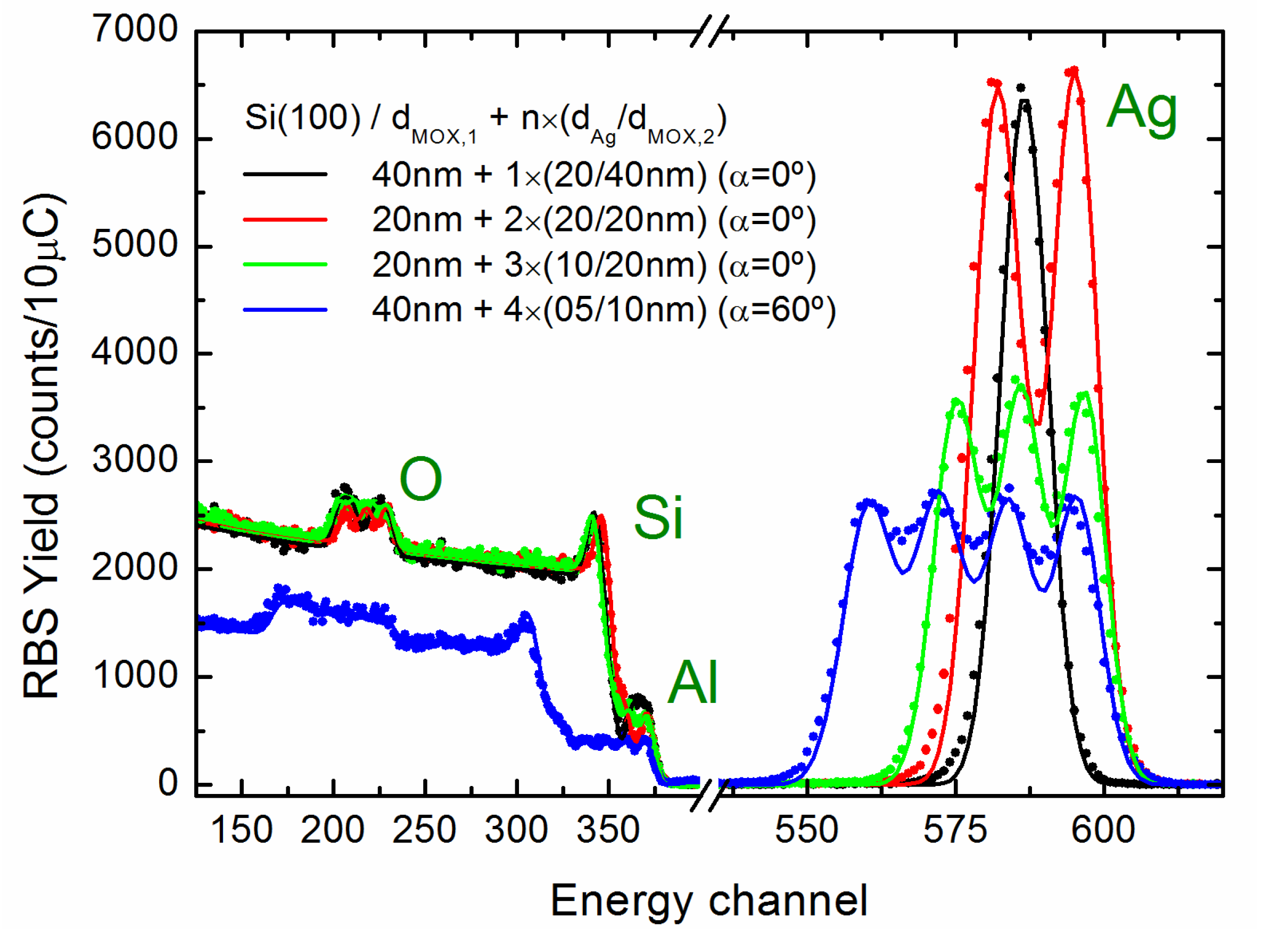
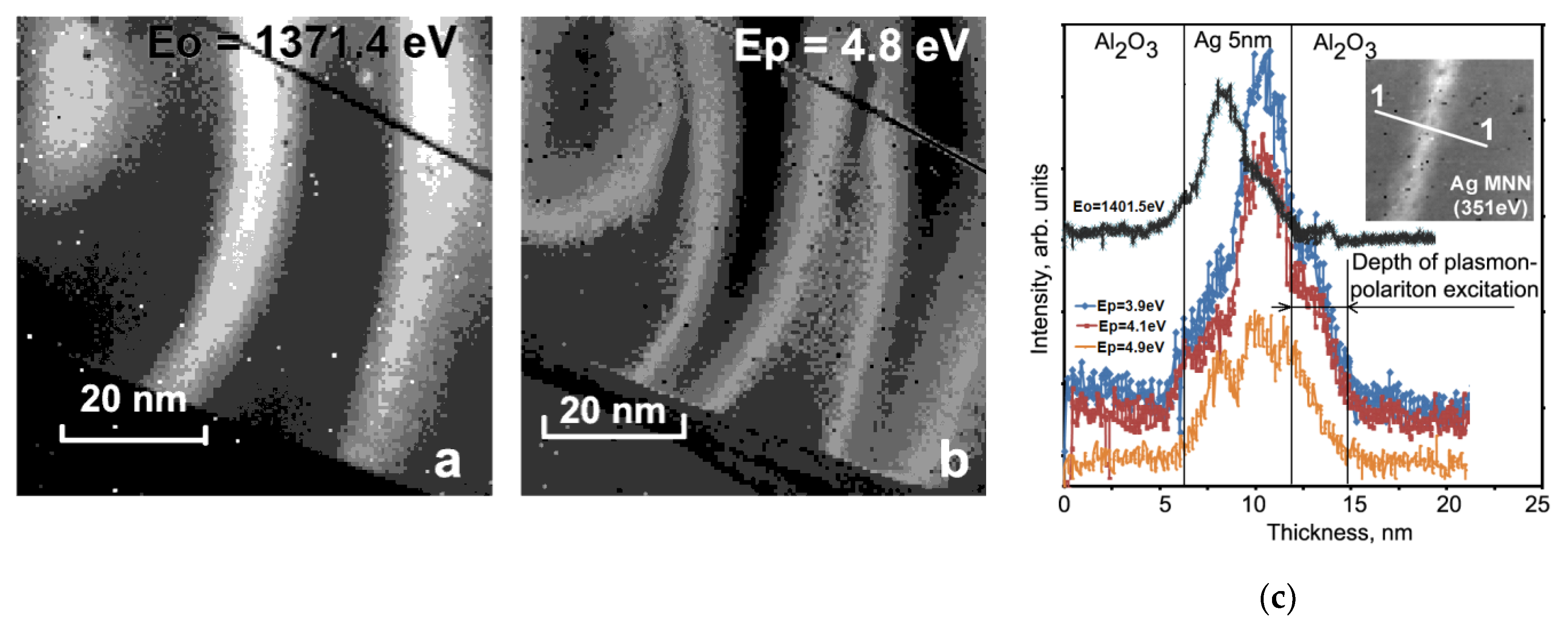
3.2. Structure of the Multilayer Coatings Revealed by Rutherford Back-Scattering

Figure 1 shows the experimental (dots) and simulated (solid lines) RBS spectra of representative Al2O3/Ag multilayer coatings. The upper energy limits corresponding to the detected signals from different elements are labelled for identification. The maximum energy of backscattered projectiles from a certain element present at the surface is given by the kinematic factor of the binary collision. For heavier elements than the projectile, this energy increases with the atomic number of the scattering centre, and therefore, backscattered particles are detected at higher energy. Events (counts) from the same element detected at a lower energy correspond to collisions taking place deeper from the surface, since part of the projectile energy is lost on the way in and out through the sample. In this way, RBS provides information about the elemental profile. Furthermore, the RBS yield for each element is proportional to the convolution of its areal density and corresponding Rutherford cross-section (which is proportional to the square of the atomic number), providing information about its concentration at certain depth.
In Figure 1, the Ag signal appears well separated on the high-energy side of the spectra due to its relatively high mass with respect to the other film-containing elements and the substrate. In addition, its high atomic number Z provides a relatively high RBS yield. In all the cases, the coatings present a top-most Al2O3 layer, and therefore, the energy maximum of the Ag signal shifts depending on the thickness of said layer due to the secondary scattering of reflected ions on electron shells of atoms located at various depths in the coating. The modulation of the Ag signal is a direct fingerprint of the multilayer structure where the number of maxima indicates the number of Ag layers (n). In order to resolve the thinnest Ag layers (5 nm), the incidence angle (α) of the probing He+ beam with respect to the surface normal was increased to 60° (larger effective layer thickness). Structure parameters were refined by comparison of experimental and simulated by SIMNRA code [29] data. The agreement between the simulated and experimental data supports the stoichiometry of the different layers and indicates the good quality of the interfaces (within the RBS resolution of ≈5nm).

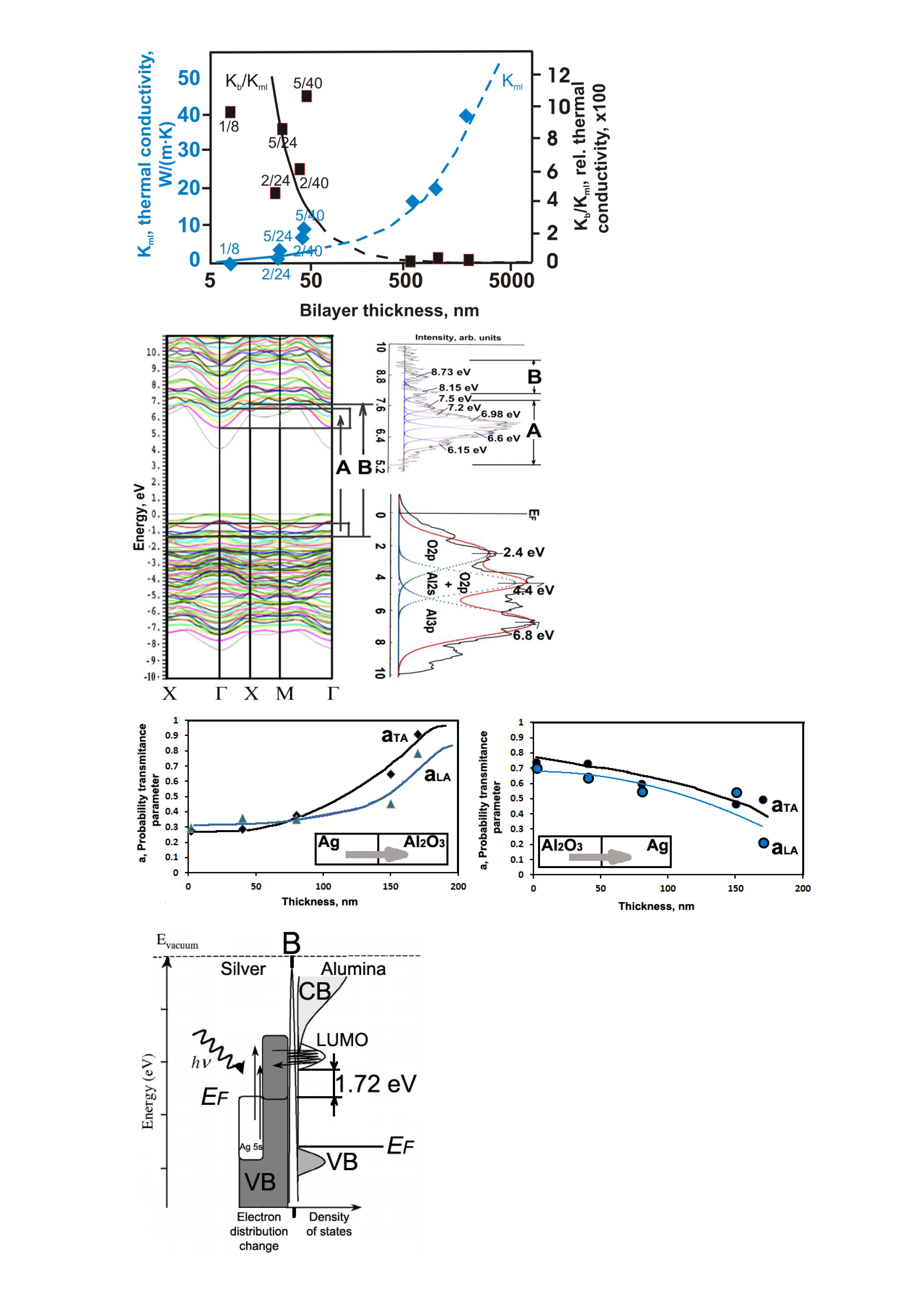
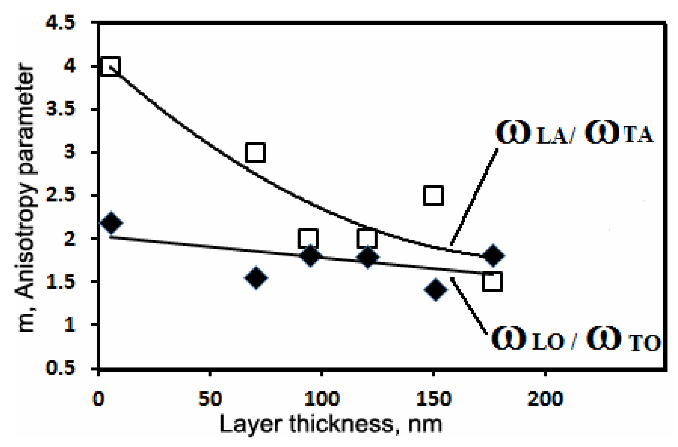
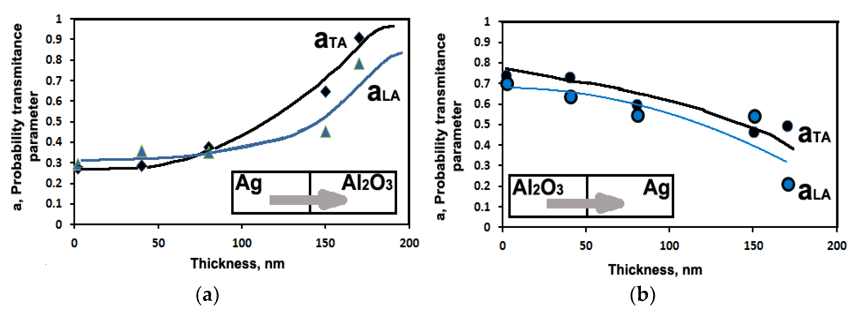
3.3. Thermal Conductivity of Multilayer Coatings and Interfaces

To estimate the role of metal-dielectric boundaries in our metal–oxide composites, we evaluated their thermal conductivity Kb in the system based on experimental measurements of thermal conductivities together with literature data on heat conductivities of Al2O3 and Ag nanolayers of different thickness using Equation (4) derived from Equation (1):
K b = 1 R b = N 1 N ( L 1 + L 2 ) K ml ( L 1 K 1 + L 2 K 2 )
Figure 2 presents heat conductivity coefficients of the multilayer coatings (Kml) and the relative contribution of interfaces (Kb/Kml) as function of the bilayer thickness. These values have been extracted from the measured thermal conductivities of the multilayered samples presented in Table 1 together with the reported thermal conductivity data for bulk and nanolayer alumina [31,33,34,35,36] and Ag [36,37,38] by interpolating and extrapolating them to the layer thicknesses of our samples. The experimental data obtained from our multilayer coatings are plotted in the region below 50 nm. The results for bilayers thicknesses above from 50 nm were calculated on the basis of literature data using Equation (1).
Thermal conductivity increases to ≈10 W/m·K when bilayer thickness increases from ≈25 nm to around 45 nm for the Ag layer thickness of 2 and 5 nm; that is approximately three times lower than thermal conductivity of alumina 28.84 W/(m·K) found in the sample 200. Therefore, an addition of the component with high thermal conductivity (KAg = 430 W/(m·K) in the “bulk” state) decreases, paradoxically, the thermal conductivity of multilayer system. As the theoretical calculation shows, the thick coating (4500 nm/4500 nm) has a high thermal conductivity of about 202.0 W/(m·K).
The average Kb value was 11.0 W/K with variation from 0.27 to 25.9 W/K. Such variation may occur due to unequal conditions of measurements and calculations in the above-mentioned sources, but the curve Kb/Kml on Figure 2 clearly illustrates the tendency in the growing role of interfaces.
One can see that interfaces make a significant input to heat transfer only in nanolaminate metal-dielectric structures with bilayers thinner than 150 nm. This trend corroborates the hypothesis that the role of interfaces becomes more relevant as materials downsize toward the nanoscale. Heat dissipation at the interface in thick multilayer coatings is considerably lesser in comparison with the thermal conductivity of the volume.
Generally, the thermal conductivity of nanosystems strongly depends on its geometry [39] or roughness regarding interfaces, but in our case we have enough perfectly smooth boundaries between layers (see Figure 1and Figure 10) to assume the same Kb values for all samples. Moreover, it will be shown below that metal–oxide and oxide–metal boundaries are not symmetric relative to heat transfer direction.

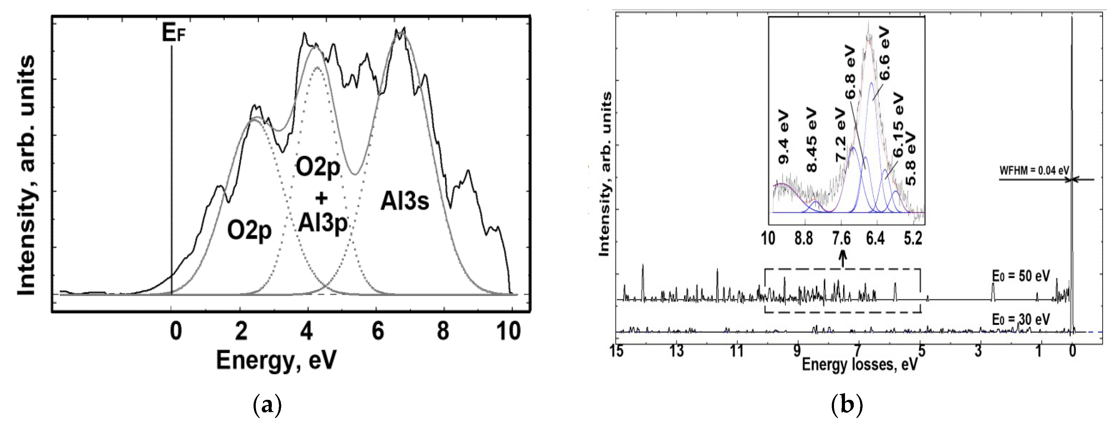
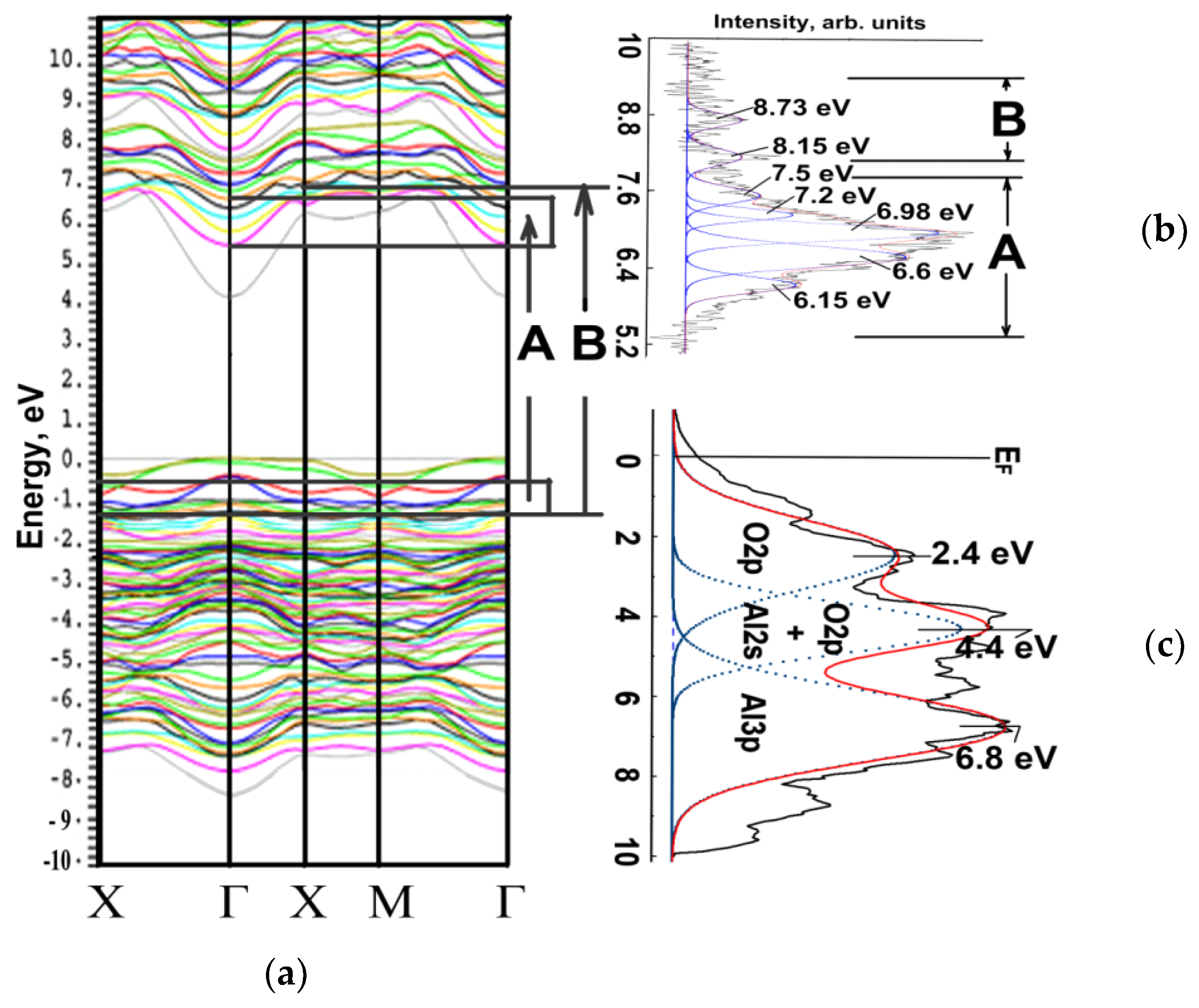
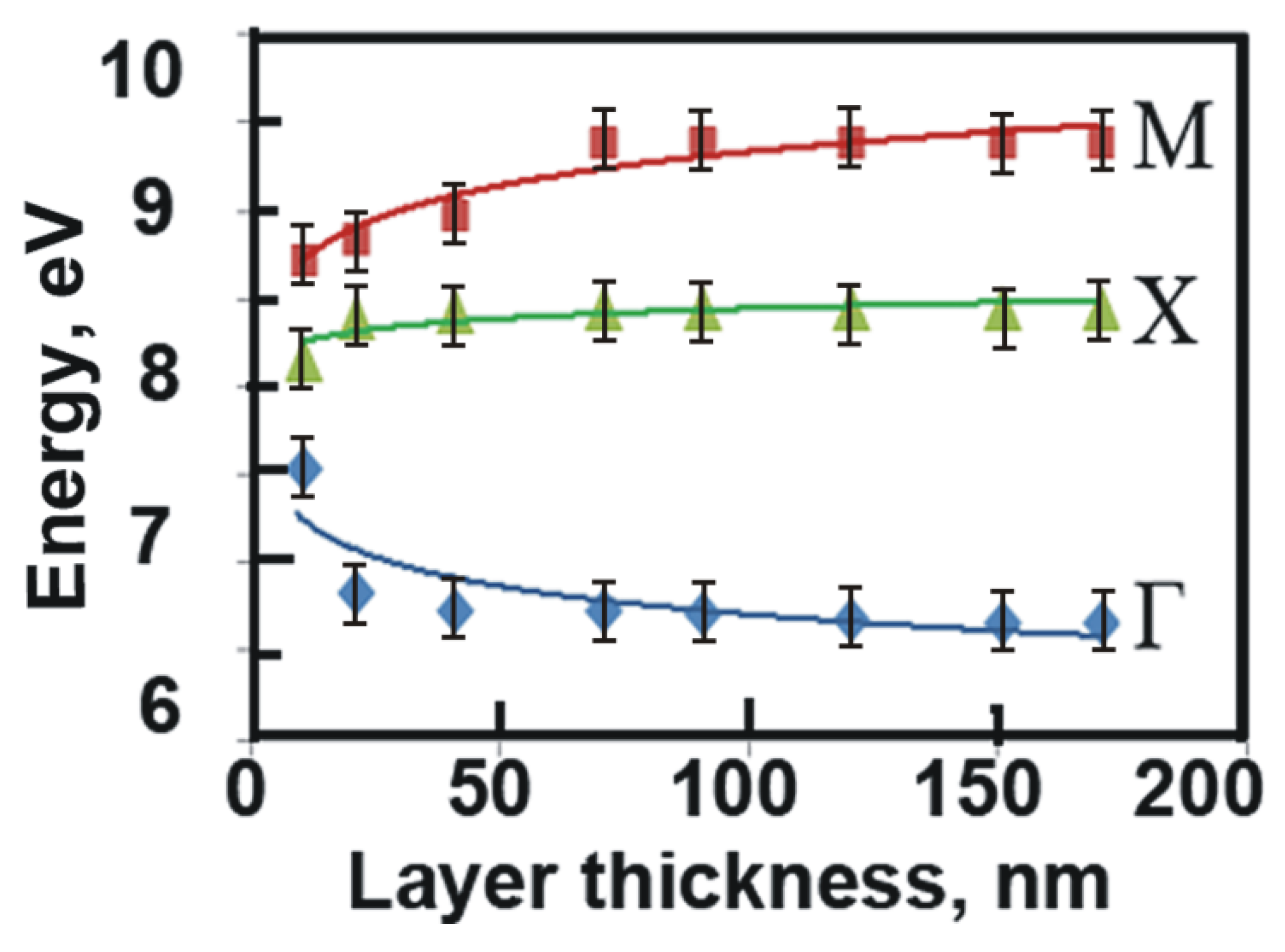
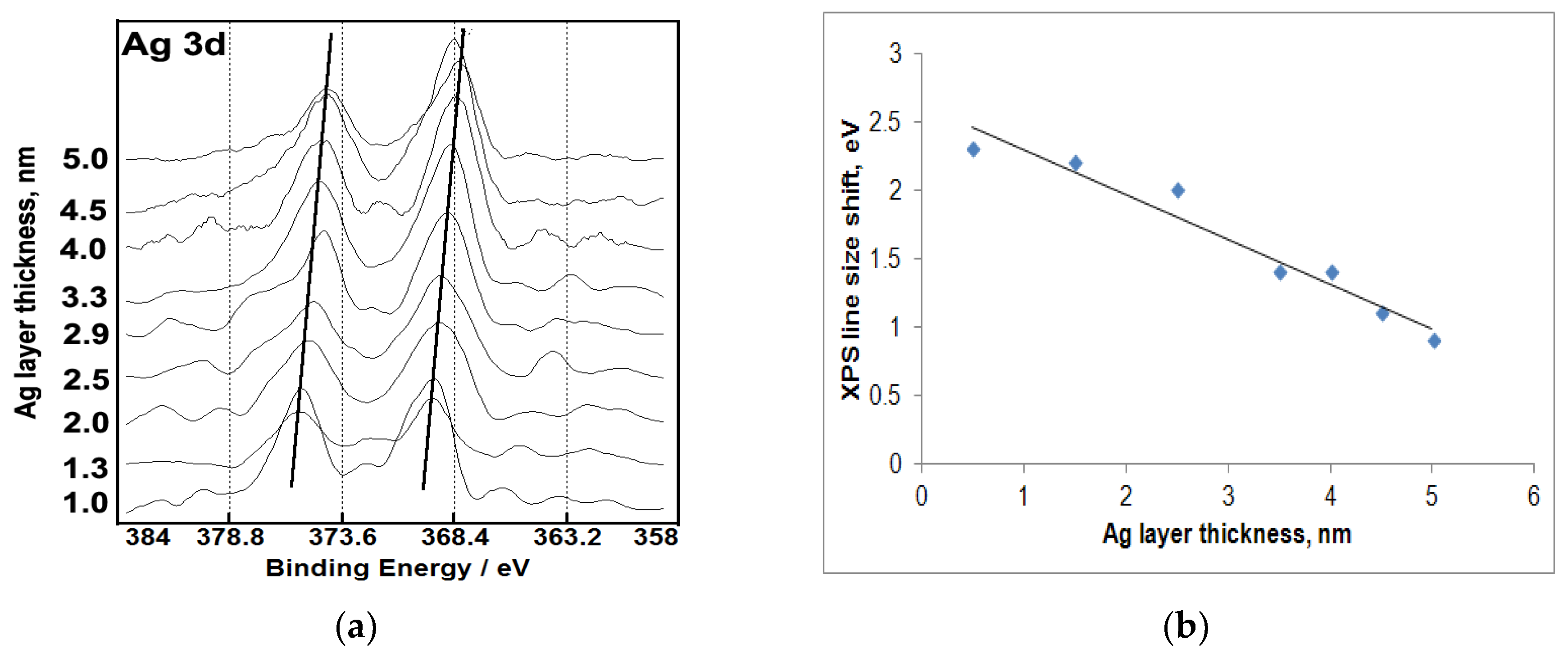
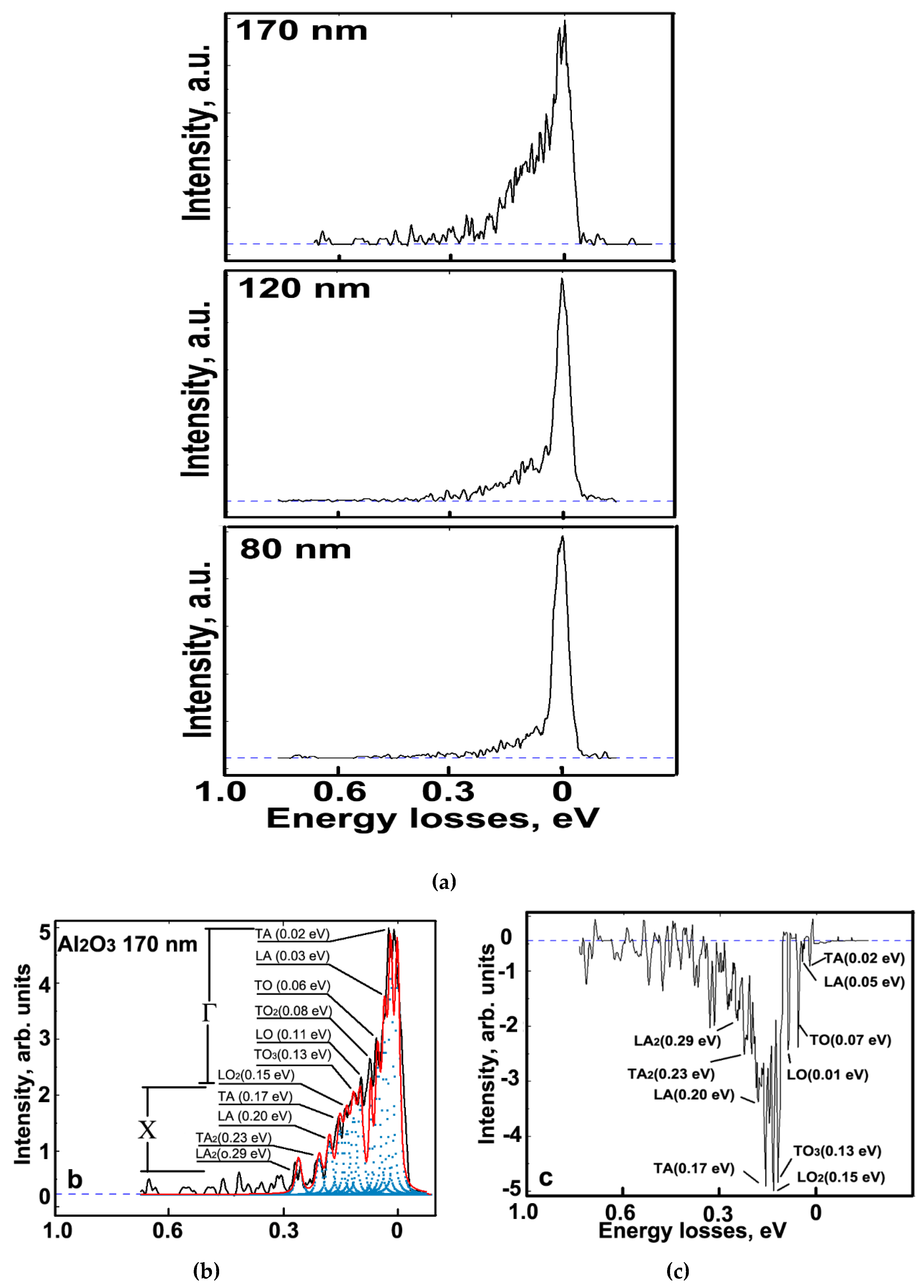
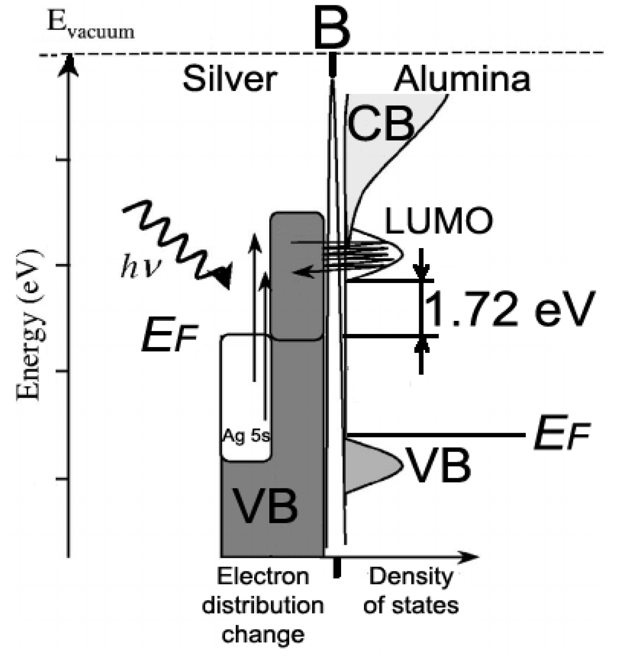
3.4. Electronic Structure and Features of Plasmon and Phonon Propagation in Al2O3/Ag Multilayer Coatings

Studies of Ag/Al2O3 nanolaminate coatings’ electronic structures and features of the phonon and plasmon oscillations’ propagations enabled explaining their anomalously low thermal conductivity.
Figure 3a shows the XPS spectrum of the Al2O3 layer valence band with individual components resolved after deconvolution and fitting. This oxide has a cubic nanocrystalline structure where oxygen states are dominant. The upper valence levels correspond to the O 2p non-bonding states, and the lower part is the O 2p bonding states mixed with the Al 3p electrons. The valence band (VB) component with maximal binding energy corresponds to Al 3s orbitals. These data are in good agreement with theoretically calculated Al2O3 band structure [40,41]. High localization of O 2p–Al 3p bonds and a small electron concentration near the Fermi level are crucial factors determining thermal properties: decreasing of electrons concentration near Fermi level limits electronic transport into conducting band and decreases electronic input in heat conductivity.
HREEL spectra from 170 nm layer Al2O3 at primary electrons energies of 30.0 and 50.0 eV are shown in Figure 3b. We shall remark that noticeable excitation of interband electronic transitions can be detected at primary electron energies over 30 eV. O 2p and Al 3p electrons form strong covalent bonds localizing far from the Fermi level. This explains the great potential of their excitation for transitions from valence to the conduction band (CB). Interband electronic transitions in the range of 5.0–10.0 eV are shown as insets in Figure 3b at the electron source energy of 50.0 eV. The fine structure of the energy transitions was fitted by Gaussian peaks. Differences in components consolidated in two groups 5.8–7.2 eV and 8.45–9.4 eV are clearly visible. The interpretation of these transitions has been made on the basis of the theoretical band structure of alumina [38]. A schematic representation of the interband electron transitions across the band gap in Al2O3 under external excitation is shown in Figure 4. The wide peak A corresponds to transitions along the Γ symmetry direction in the Brillouin Zone (reciprocal lattice). The B peaks appear as a result of the transitions of O2p valence electrons in the conduction band in the directions X and M.
The HREELS and XPS data enable estimating the influence of nanostructuring on the width of the band gap. For the case of Al2O3 170 nm layer, the width of band gap which separates the valence and conduction bands corresponds to 5.8–7.2 eV at Γ symmetry point. The theoretical value for the Γ direction of Al2O3 band gap is 7.2 eV, as found by Mousavi at al. [42]. According to [43], the minimal width of the band gap in Γ symmetry point is 4.2 eV. Our experimental value of the band gap is very close to the theoretical one. Intensities of HREELS components in the A band correspond to the calculated density of states in the CB.
Figure 5 demonstrates that energies of interband transitions are decreased in the X and M directions and increased along the direction Γ while Al2O3 layers are thinned from 170 nm to 10 nm. This shift is small but detectable. Therefore, the band gap is aligned in alumina layers thinner than approximately 50 nm. The FWHM of HREELS peak characterizing the interband transition in Γ direction is 0.80 eV. This relatively large width of the “A” HREELS line indicates that there is good mobility for electrons if they only could jump over wide band gap.
The electronic structure of silver was also changed with nanostructuring. Binding energies of inner Ag 3d levels are increased with thinning Ag layers in the Ag/Al2O3 multilayer coating (Figure 6). A similar appearance was observed earlier in nanocrystals and layers of various materials with refinements of their characteristic sizes at the nanoscale [20,21,22,26]. The decreasing of Ag thickness induces notable changes in valence band of Ag [26]. Fermi level is shifted deeper and DOS near EF is decreased. In a thin film state, a metal acquires the properties of the dielectric. One can assume that transformations in the electronic structure of Al2O3 and Ag are naturally affected by plasmons and phonons propagation in the volume and near interfaces, contributing to the general mechanism of heat transfer.
The original and deconvoluted vibrational (phonon) spectra from 170, 120, and 80 nm Al2O3 layers obtained by ion beam thinning of the 200 nm Al2O3 protective layer above the Ag/Al2O3 multilayers are shown on Figure 7. Alumina has a rhombohedral elementary cell containing 10 atoms, and therefore, 30 phonon branches (modes) could be excited [44]. The HREELS can resolve only a small part of the strongest vibrations. The intensity of phonon spectra is decreased with thinning of the alumina layer. One can see on Figure 7b that experimental HREELS spectra have a complex structure, containing acoustic (TA) and optical (TO) components in two (Γ and X) symmetry directions in the Brillouin zone. Deconvolution and subtracting one spectrum (170 nm) from the other one (80 nm) amplifies some of the finest changes of phonon propagation with the decreasing of Al2O3 layer thickness. The resulting spectrum in Figure 7c shows that first acoustic oscillations are slightly reduced in intensity when layer thickness is decreased from 170 nm to 80 nm. The first and second harmonics of longitudinal (LO) and transverse (TO) optical oscillations of Γ and X directions are attenuated significantly in the 80 nm layer relatively to 170 nm one. Comparing optical and acoustic vibrations, one can see that the first is attenuated stronger. The higher-order harmonics are attenuated in thin layers. When decreasing the layer thickness to 2.0 nm, the acoustic and optical phonon peaks are shifted to shorter wavelengths. This “blue shift” can be clearly seen at layers thicknesses below 80.0 nm, which corresponds to results reported in [41].
This phenomenon was dissimilar for acoustic and optical excitations with different polarizations. Figure 8 depicts changes of anisotropy parameters for acoustic (mA) and optical (mO) phonon modes calculated through expressions:
mA = ωLATA
and
mO = ωLOTO.
The anisotropy of acoustic modes increases noticeably in insulator layers thinner than 80 nm, while frequencies of LO and TO vibrations have smaller dependencies on layers thickness. The blue shift of transverse acoustic (TA) phonons was more visible than longitudinal (LA) ones at decreased thicknesses of the oxide layer. TA phonon decay is faster in thin layers than in thick ones. That is, the TA phonon coupling is increased mostly in the 8 nm layer. It is most likely that such obvious and significantly sized effects are connected to the traditional relationship of phonon mean free path (MFP) with the geometric (crystallographic) parameters of the Al2O3 layer structure. According to [40], the anisotropy factor of acoustic phonons in Al2O3 single crystal is approximately 1.13. In our case, the parameter “m” is slightly higher, and it increases significantly in thin films due to anisotropic phonon scattering. As this phenomenon is observed at frequencies controlling heat transport, it will undoubtedly have an effect on the anisotropy of alumina thermal conductivity.
Heat dissipation in heterophase materials occurs not only in the volume, but also at interfaces. In the multilayer nanocomposite, the interfacial thermal resistance plays a critical role for the heat transport. When Phase 1 is Al2O3 and Phase 2 is Ag, the phonon transmittance probability enables characterizing the energy transfer across the interface [45]:
a 1 , j ( ω ) = ν 2 , j . g 2 , j ( ω ) ν 1 , j . g 1 , j ( ω ) + ν 2 , j . g 2 , j ( ω )
where a1,j is phonon transmission probability of mode j in phase 1; ω is phonon angular frequency; vi,j is phonon velocity of mode j in phase I; and gi,j (ω) is the phonon density of states of mode j in side i. The latter corresponds to the intensity of the ith phonon peak on the HREEL spectrum.
The phonon velocity was calculated from
νi = ωi(GHz⋅sec−1)/qi
where q1 is wavevector for the trigonal A12O3 Brillouin zone f. A vector magnitude of 14.5 rad·nm−1 was calculated to be nearly perpendicular to the XY plane [40]; q2 is a lattice vector of Ag   ( Γ Γ Λ ) = 3 π a = 13 . 3   rad   nm 1 , where Ag lattice constant a = 0.4085 nm. The experimental phonon frequencies (ωTA, LA for Ag) and intensities of REEL spectral components (gTA, LA for Ag) were previously obtained experimentally in [26]. Thicknesses of silver layers were chosen equal to alumina ones.
Figure 9 demonstrates that phonons’ transmittance through the interface depends on layer thickness and direction of energy transfer. These graphs were calculated based on experimental analysis of the phonon resonance in Ag and Al2O3 layers to interpret phonon propagation across boundaries in accordance with the model of Equations (5) and (6). Phonon transmittance across the metal-isolator interface is very minor and follows approximately a linear relation for layer thickness from 80.0 to 2.0 nm. While the layers’ thickness is over 100 nm, the probability of transboundary transmittance increases nonlinearly. These changes are similar for each type of phonon polarization. In contrast, the probability of boundary energy transmission in the opposite (dielectric → metal) direction decreases monotonically with increasing thickness of the layers.
In this case, the observed dimensional dependence cannot be explained by the traditional comparison of MFP and layer thickness. Perhaps such a complex and ambiguous nature of energy transfer across the boundary occurs is due to differences in the polarization vector and the phonon energy in each of these cases. The observed size effect of transboundary phonon propagation allows us to explain the enhanced barrier role of interfaces in energy transfer within the multilayer coatings. Probability of phonon heat transfer from silver nanolayers to alumina is extremely low for thin layers. From other side, taking into account that the phonon part of heat transfer in metals is several tens of times lesser than the plasmon mechanism, we can assume that phonon mechanism is substantially weakened in heterophase structures with nano-sized layers. Therefore, we need to study the plasmon contribution to the propagation of heat in the multilayer nanocomposites.
Figure 10a–c display SEM images of angle lap of the 5/24 nm Ag/Al2O3 coating acquired with back scattered electrons (E0 = 1371.4 eV), plasmon mapping at energy loss Ep = 4.80 eV, Ag MNN Auger imaging (AEM), and line distribution of plasmon intensity along 1–1 line on AEM. On the BEI of Figure 10a, the white contrast is formed in the silver layers; dark areas correspond to alumina. The map of symmetric plasmon excitation with energy of 4.8 eV and the same linear distribution at plasmon energy 4.9 eV are shown in Figure 10b,c. Symmetric or antisymmetric types of plasmon excitation depend on the plasmon energy and thickness of Ag layers. The antisymmetric resonance is observed in layers thicker than 5 nm, while the symmetrical character occurs most likely in a thin metal layer. Figure 10c shows the evolution of plasmon intensity at different energies as the electron probe is line-scanned along the 1–1 direction on the AEI (insert on Figure 10c). The plasmon intensity and its lateral distribution depend on the resonance energy. Plasmons are excited symmetrically or antisymmetrically in the silver layer depending on their excitation energy. These experimental observations are in very good agreement with theoretical calculations [46].
Antisymmetric plasmon excitations at 3.9 and 4.1 eV are propagated along phase boundaries. These plasmons are penetrated into the dielectric layer at some depth (h) through the interface due to plasmon-polariton (SPP) interactions. This non-uniform resonance structure is a consequence of confinement of electromagnetic DOS in thin planar nanocomposite. Such a spatial distribution is originated from the confinement of electromagnetic DOS in thin planar nanocomposite. Similar spatially inhomogeneous maps of plasmon excitations were observed earlier in silver nanocrystals with a semi-empirical investigation [47]. The plasmon-polariton penetration into dielectric layers reaches 2.0–5.0 nm, and depends on plasmon energy and excitation intensity. Polariton excitation is the most important stage of electronic heat transfer from metal to dielectric. The depth of plasmon-polariton penetration is the most important characteristic of heat transfer. We assume that the excitation of valence electrons of Al2O3 with an electromagnetic “plasmon” field existing in the Ag boundary layer is doubtful. Figure 3a demonstrates that O 2p and Al 2s valence electrons are strongly hybridized. The DOS at the Fermi level is negligible. Interband electron transitions in Al2O3 can be realized by external energy pumping with sufficient power. On the other hand, we know that the Schottky barrier measured in [48] for an Ag layer with 35 nm Al2O3 film thickness is equal to 1.72 eV; it significantly decreases the energy barrier for electron transitions from Ag VB to Al2O3 CB by external energy pumping (Figure 11).
We assume the mechanism of plasmon–polariton interaction is as follows. We can suppose that Ag conducting electrons are injected into the CB of the insulator by an external energy source and a boundary electromagnetic field that arises at plasmon resonance. Upon colliding at the interface, the excited Ag CB electrons (which may be hot electrons of the plasmon excitation) are temporarily transferred to the Al2O3 CB and back again. In this qualitative picture, the energy difference between CB of Ag and alumina layers is levelled by the Schottky potential. In addition, interfaces are playing a complex role in a heat transfer process. The increment of heat in alumina with transferred electrons can be dissipated by their return to the Ag layer. This process is controlled by interface scattering; returned electrons will be involved in plasmon excitation, etc. As we have shown in Figure 10b,c, the spatial distribution of plasmon excitations is very complex near boundaries and in nanosized volumes. On one hand, the contact of Ag with alumina promotes heat transfer by the electronic mechanism, and on the other hand, confinement and amplification of inelastic scattering by the interface greatly weakens this heat flux. In planar nanostructures materials, its heat conductivity will decrease until only electron tunnelling is permitted. Tunnelling of electrons between Ag layers will suddenly and radically increase the thermal conductivity of the material when the thickness of Al2O3 reaches several nm or less [49].

4. Conclusions

The anomalous reduction of thermal conductivity in nanolaminate multilayer Ag/Al2O3 coating in comparison with bulk components is explained by the influence of confinement on plasmons and phonons’ propagation. This is based on a considerable decline of heat conductivity in the set of nanoscaled Ag/Al2O3 multilayered coatings with individual layer thickness decreasing from 170 to 1 nm. Nanostructuring influences the electronic structures of metal and insulator layers. Binding energies of electrons on inner levels in Ag atoms increase, and this localization of electrons reduces the metal character of interatomic bonds when the layer thickness is decreased. The band gap in alumina evolves oppositely in points Γ and X of zone structure at layer thinning: in 170 nm layer, these values correspond to 6.6 and 8.45 eV; and they are changed to 6.9 and 8.15 eV in 24 nm layers and to 8.20 and 7.5 eV in 10 nm layers, accordingly. The size effect of nanostructuring is expressed by the increasing of the effective band gap due to its smoothing.
The contribution of phonon propagation to the heat transfer mechanism in Ag/Al2O3 nanolayer composites has several features. The process obeys the classical picture when thinning of layers below the phonon MFP in the nanometer range reduces the intensity of energy transport by phonons. Anisotropy of acoustic phonons’ propagation rises when reducing the individual layers in the multilayer coating. Furthermore, the probability of phonon transmittance across Ag/Al2O3 interfaces significantly decreases with layer thinning. On the contrary, the probability of opposite phonon transportation in direction Al2O3/Ag increases. Despite such a complex physical picture, the contribution of the interface phonon heat transfer to the overall balance is very small, but it increases with decreasing layer thickness.
Plasmon resonance propagates in the volume of the metal in a symmetric or antisymmetric manner depending on the excitation energy and thickness of silver layers surrounded by alumina. This non-uniform resonance structure is a consequence of the confinement of electromagnetic density of states in a thin planar nanocomposite. The plasmon–polariton interaction propagates 2.0–5.0 nm into Al2O3, and depends proportionally on the intensity of plasmon excitation in Ag. Plasmon–polariton propagation is the main electronic mechanism of heat transfer. Electronic DOS at EF in alumina is too low to rise above the wide band gap by internal interband transitions. Polariton resonance results in injection of Ag 5s electrons into CB of Al2O3 by energy pumping and the boundary electromagnetic field generated by plasmon resonance. The layer thinning in the investigated multilayer coatings complicates plasmons and phonons’ propagation in layers, and at interfaces and it is a key reason for the sharp heat conductivity lessening.

Author Contributions

Conceptualization, A.K., D.W., and J.L.E.; investigation, D.W., A.K., V.V., and R.G.; formal analysis, V.V.; visualization, D.W., A.K., and V.V.; writing—original draft preparation, D.W. and A.K.; writing—review and editing, D.W., A.K., V.V., R.G., and J.L.E. All authors have read and agreed to the published version of the manuscript.

Funding

The research was carried out with partial financial support of RSF, project number 14-12-00170 (in part, for the fabrication and characterization of Al2O3/Ag coatings) and RFBR project number 16-08-00527 (modelling of plasmons and phonons propagation).

Conflicts of Interest

The authors declare no conflict of interest.

References

  1. Mosquera, A.A.; Horvat, D.; Rashkovskiy, A.; Kovalev, A.; Miska, P.; Wainstein, D.; Allbella, J.; Endrino, J.L. Exciton and core-level electron confinement effects in transparent ZnO thin films. Sci. Rep. 2013, 3, 1714. [Google Scholar] [CrossRef] [Green Version]
  2. Gao, Y.; Zhao, X.; Yin, P.; Gao, F. Size-Dependent Raman Shifts for nanocrystals. Sci. Rep. 2016, 6, 20539. [Google Scholar] [CrossRef] [PubMed]
  3. Yao, K.; Liu, Y. Plasmonic metamaterials. Nanotech. Rev. 2014, 3, 177–210. [Google Scholar] [CrossRef] [Green Version]
  4. Sun, J.; Shalaev, M.I.; Litchinitser, N.M. Experimental demonstration of a non-resonant hyperlens in the visible spectral range. Nat. Commun. 2015, 6, 7201. [Google Scholar] [CrossRef] [Green Version]
  5. Callebaut, H.; Kumar, S.; Williams, B.S.; Hua, Q.; Reno, J.L. Importance of electron-impurity scattering for electron transport in terahertz quantum-cascade lasers. Appl. Phys. Lett. 2004, 84, 645–647. [Google Scholar] [CrossRef] [Green Version]
  6. Shen, X.; Cui, T. Planar plasmonic metamaterial on a thin film with nearly zero thickness. Appl. Phys. Lett. 2013, 102, 211909. [Google Scholar] [CrossRef]
  7. Tian, Z.; Esfarjani, K.; Shiomi, J.; Henry, A.S.; Chen, G. On the importance of optical phonons to thermal conductivity in nanostructures. Appl. Phys. Lett. 2011, 99, 053122. [Google Scholar] [CrossRef]
  8. Kargar, F.; Ramirez, S.; Debnath, B.; Malekpour, H.; Lake, R.; Balandin, A.A. Acoustic Phonon Spectrum and Thermal transport in Nanoporous Alumina Arrays. Appl. Phys. Lett. 2015, 107, 171904. [Google Scholar] [CrossRef] [Green Version]
  9. Toberer, E.S.; Baranowski, L.L.; Dames, C. Advances in thermal conductivity. Annu. Rev. Mater. Res. 2012, 42, 179–209. [Google Scholar] [CrossRef]
  10. Cahill, D.G. Nanoscale thermal transport. Appl. Phys. Rev. 2014, 1, 011305. [Google Scholar] [CrossRef] [Green Version]
  11. Balandin, A.A.; Denis, L.N. Phononics in low-dimensional materials. Mater. Today 2012, 15, 266–275. [Google Scholar] [CrossRef]
  12. Bell, L.E. Cooling, heating, generating power, and recovering waste heat with thermoelectric systems. Science 2015, 321, 1457–1461. [Google Scholar] [CrossRef] [PubMed] [Green Version]
  13. Biswas, K. High-performance bulk thermoelectrics with all-scale hierarchical structures. Nature 2012, 489, 414–418. [Google Scholar] [CrossRef] [PubMed]
  14. Oraizi, H.; Abdolali, A. Design and optimization of planar multilayer antireflection metamaterial coatings at KU band under circularly polarized oblique plane wave incidence. Prog. Electromagn. Res. C 2008, 3, 1–18. [Google Scholar] [CrossRef] [Green Version]
  15. Chen, J.; Zhang, G.; Li, B. Impacts of Atomistic Coating on Thermal Conductivity of Germanium Nanowires. Nano Lett. 2012, 12, 2826–2832. [Google Scholar] [CrossRef] [Green Version]
  16. Moldovan, M. Phonon wave interference and thermal bandgap materials. Nat. Mater. 2015, 14, 667–674. [Google Scholar] [CrossRef]
  17. Chou, Y.-H.; Wu, Y.; Hong, K.-B.; Chou, B.-T.; Shih, J.-H.; Chung, Y.-C.; Chen, P.-Y.; Lin, T.-R.; Lin, C.-C.; Lin, S.-D.; et al. High-operation-temperature plasmonic nanolasers on single-crystalline aluminum. Nano Lett. 2016, 16, 3179–3186. [Google Scholar] [CrossRef]
  18. Ordonez-Miranda, J.; Tranchant, L.; Chalopin, Y.; Antoni, T.; Volz, S. Thermal conductivity of nano-layered systems due to surface phonon-polaritons. Journ. Appl. Phys. 2015, 115, 054311. [Google Scholar] [CrossRef] [Green Version]
  19. Chen, D.Z.A.; Narayanaswamy, A.; Chen, G. Enhancement of in-plane thermal conductivity of thin films via surface phonon-polaritons. Proceedings of IMECE2005 ASME International Mechanical Engineering Congress and Exposition, Orlando, FL, USA, 5–11 November, 2005; pp. 841–846. [Google Scholar]
  20. Kovalev, A.I.; Wainstein, D.L.; Rashkovskiy, A.Y.; Osherov, A.; Golan, Y. Size shift of XPS lines observed from PbS nanocrystals. Surf. Interf. Anal. 2010, 42, 850–854. [Google Scholar] [CrossRef]
  21. Kovalev, A.I.; Wainshtein, D.L.; Rashkovskiy, A.Y.; Golan, Y.; Osherov, A.; Ashkenazy, N. Studying of Quantum-Size Effects Origination in Semiconducting Lead Sulfide Nanocrystals. Protect. Met. Phys. Chem. Surf. 2010, 46, 633–638. [Google Scholar] [CrossRef]
  22. Kovalev, A.; Wainstein, D.; Rashkovskiy, A.; Golan, Y.; Osherov, A.; Ashkenasi, N. Complex investigation of electronic structure transformations in Lead Sulfide nanoparticles using a set of electron spectroscopy techniques. Vacuum 2012, 86, 638–642. [Google Scholar] [CrossRef]
  23. Wainstein, D.L.; Kovalev, A.I. Regularities of electronic structure transformations in nanomaterials with decreasing their characteristic size. J. Phys. Conf. Ser. 2017, 857, 012055. [Google Scholar] [CrossRef] [Green Version]
  24. Kovalev, A.I.; Wainstein, D.L.; Rashkovskiy, A.Y.; Gago, R.; Soldera, F.; Endrino, J.L.; Fox-Rabinovich, G.S. Interface-Induced Plasmon Nonhomogeneity in Nanostructured Metal-Dielectric Planar Metamaterial. J. Nanomat. 2015, 2015, 231–240. [Google Scholar] [CrossRef]
  25. Kovalev, A.I.; Rashkovskiy, A.Y.; Wainstein, D.L.; Gago, R.; Soldera, F.; Endrino, J.L. Influence of electronic structure, plasmon-phonon and plasmon-polariton excitations on anomalously low heat conductivity in TiAlN/Ag nanoscale multilayer coatings. Curr. Appl. Phys. 2016, 16, 459–468. [Google Scholar] [CrossRef]
  26. Kovalev, A.I.; Wainstein, D.L.; Rashkovskiy, A.Y.; Gago, R.; Soldera, F.; Endrino, J.L. The confinement of phonon propagation in TiAlN/Ag multilayer coatings with anomalously low heat conductivity. Appl. Phys. Lett. 2016, 108, 223106. [Google Scholar] [CrossRef] [Green Version]
  27. Gago, R.; Soldera, F.; Huebner, R.; Lehmann, J.; Munnik, F.; Vázquez, L.; Redondo-Cubero, A.; Endrino, J.L. X-ray absorption near-edge structure of hexagonal ternary phases in sputter-deposited TiAlN films. J. Alloys Compd. 2013, 561, 87–94. [Google Scholar] [CrossRef]
  28. Mayer, M. SIMNRA User’s Guide 6.05; Max-Planck-Institut für Plasmaphysik: Garching, Germany, 2009. [Google Scholar]
  29. Cahill, D.G. Analysis of heat flow in layered structures for time-domain thermoreflectance. Rev. Sci. Instrum. 2004, 75, 5119–5122. [Google Scholar] [CrossRef]
  30. Josell, D.; Bonevich, J.E.; Nguyen, T.M.; Johnson, R.N. Heat transfer through nanoscale multilayered thermal barrier coatings at elevated temperatures. Surf. Coat. Tech. 2015, 275, 75. [Google Scholar] [CrossRef]
  31. Jain, A.; McGaughey, A.J.H. Thermal transport by phonons and electrons in aluminum, silver, and gold from first principles, Supplementary Information. Phys. Rev. B 2016, 93, 081206. [Google Scholar] [CrossRef] [Green Version]
  32. Majumdar, A. Microscale heat conduction in dielectric thin films. ASME HTD 1991, 184, 34–41. [Google Scholar] [CrossRef]
  33. Jennifer Su, Y.; Wang, H.; Porter, W.D.; De Arellano Lopez, A.R.; Faber, K.T. Thermal conductivity and phase evolution of plasma-sprayed multilayer coatings. J. Mater. Sci. 2001, 36, 3511–3518. [Google Scholar]
  34. Luo, Z.; Liu, H.; Feng, Y.; Ye, P.; Chen, Y.; Xu, X. In-plane thermal conductivity of ultra-thin Al2O3 films measured by Micro-Raman. In Proceedings of the ASME 2013 Heat Transfer Summer Conference HT2013, Minneapolis, MN, USA, 14–19 July 2013; pp. HT2013–17170. [Google Scholar]
  35. Stark, I.; Stordeur, M.; Syrowatka, F. Thermal conductivity of thin amorphous alumina films. Thin Solid Films 1993, 226, 185–190. [Google Scholar] [CrossRef]
  36. Cappella, A.; Battaglia, J.-L.; Schick, V.; Kusiak, A.; Lamperti, A.; Wiemer, C.; Hay, B. High temperature thermal conductivity of amorphous Al2O3 thin films grown by low temperature ALD. Adv. Eng. Mater. 2013, 15, 9999. [Google Scholar] [CrossRef]
  37. Heino, P.; Ristolainen, E. Thermal conduction at the nanoscale in some metals by MD. Microelectron. J. 2003, 34, 773–777. [Google Scholar] [CrossRef]
  38. Ryu, S.; Juhng, W.; Kim, Y. Effect of microstructure on thermal conductivity of Cu, Ag thin films. J. Nanosci. Nanotechnol. 2010, 10, 3406–3411. [Google Scholar] [CrossRef]
  39. Cocemasov, A.I.; Nika, D.L.; Fomin, V.M.; Grimm, D.; Schmidt, O.G. Phonon-engineered thermal transport in Si wires with constant and periodically modulated cross-sections: A crossover between nano- and microscale regimes. Appl. Phys. Lett. 2015, 107, 011904. [Google Scholar] [CrossRef]
  40. Perevalov, T.V.; Shaposhnikov, A.V.; Gritsenko, V.A.; Wong, H.; Han, J.H.; Kim, C.W. Electronic structure of α- Al2O3: Ab initio simulations and comparison with experiment. JETP Lett. 2007, 85, 165–168. [Google Scholar] [CrossRef]
  41. Liu, D.M.; Tuan, W.H. Microstructure and thermal conduction properties Al2O3-Ag composites. Acta mater. 1996, 44, 813–818. [Google Scholar] [CrossRef]
  42. Mousavi, S.J.; Abolhassani, M.R.; Hosseini, S.M.; Sebt, S.A. Comparison of electronic and optical properties of the α and κ phases of alumina using density functional theory. Chin. J. Phys. 2009, 47, 862–873. [Google Scholar]
  43. Yazdanmehr, M.; Asadabadi, S.J.; Nourmohammadi, A.; Ghasemzadeh, M.; Rezvanian, M. Electronic structure and bandgap of γ-Al2O3 compound using mBJ exchange potential. Nanoscale Res. Lett. 2012, 7, 488. [Google Scholar] [CrossRef] [Green Version]
  44. Bialas, H.; Stolz, H.J. Lattice dynamics of sapphire (corundum). Part I: Phonon dispersion by inelastic neutron scattering. Z. Physik B 1975, 21, 319–324. [Google Scholar] [CrossRef]
  45. Zhu, K.-R.; Zhang, M.-S.; Chen, Q.; Yin, Z. Size and phonon-confinement effects on low-frequency Raman mode of anatase TiO2 nanocrystal. Phys. Lett. A 2005, 340, 220–227. [Google Scholar] [CrossRef]
  46. Henrique, T.M.C.; Baltar, M.; Drozdowicz-Tomsia, K.; Goldys, E.M. Propagating surface plasmons and dispersion relations for nanoscale multilayer metallic-dielectric films. In Plasmonics-Principles and Applications; Kim, Y., Ed.; InTech: Moscow, Ruassia, 2012. [Google Scholar]
  47. Nelayah, J.; Kociak, M.; Stéphan, O.; Javier García de Abajo, F.; Tencé, M.; Henrard, L.; Taverna, D.; Pastoriza-Santos, I.; Liz-Marzán, L.M.; Colliex, C. Mapping surface plasmons on a single metallic nanoparticle. Nat. Phys. 2007, 3, 348–353. [Google Scholar] [CrossRef]
  48. Singh, K.; Hammond, S.N.A. Current-voltage characteristics and photoresponse of metal-metal devices. Turk. J. Phys. 1998, 22, 315. [Google Scholar]
  49. Zhang, P. Scaling for quantum tunneling current in nano- and subnano-scale plasmonic junctions. Sci. Rep. 2015, 5, 9826. [Google Scholar] [CrossRef] [Green Version]
Figure 1. RBS experimental (dots) and simulated (solid lines) spectra from representative multilayer coatings (see label for each structure). The multilayer structure can be extracted from the modulation of the Ag signal. In order to resolve the thinnest Ag layers (5 nm), the incidence angle (α) of the probing He+ beam with respect to the surface normal was increased to 60° (larger effective layer thickness). The agreement between the simulated and experimental data indicates the good quality of the interfaces.
Coatings 10 00260 g001
Figure 2. Influence of the Ag/Al2O3 bilayer thickness on the thermal conductivity coefficients of the multilayer coatings (Kml), and the relative thermal conductivity of interfaces (Kb/Kml). The values below 50 nm (solid line) correspond to the experimental data from this work; corresponding points are marked with sample codes. Values above 50 nm (dashed line) are results of calculations by using Equation (1) and literature data.
Coatings 10 00260 g002
Figure 3. Fine structure of 170 nm Al2O3 layer valence band obtained by XPS (a) and interband transitions spectra, excited by primary electron beams with energies of 30 and 50 eV (b). The full width at half maximum (FWHM) of the back scattered electron peak is 40 μeV. The dotted lines are displaying fitted components of valence electrons and interband transitions.
Coatings 10 00260 g003
Figure 4. Interpretation of HREELS fine structure. Calculated density of states (DOS) of Al2O3 (a) based on data from [32]; energy loss spectrum (b) and valence band (c) 20 nm layer of Al2O3.
Coatings 10 00260 g004
Figure 5. Energy positions of HREELS intensive peaks characterizing interband transitions in Γ, X, and M symmetry directions in the Brillouin zone of Al2O3 layers.
Coatings 10 00260 g005
Figure 6. Size shift of Ag 3d binding energies relative to the Ag reference: the set of photoelectron lines from Ag layers with different thicknesses (a); size shifts as functions of Ag layer thickness (b).
Coatings 10 00260 g006
Figure 7. Comparison of phonon HREEL spectra of 170, 120, and 80 nm Al2O3 layers (a); fine structure of phonon spectra in 170 nm Al2O3 layer (b); the differentiation of HREELS acquired from 80 nm and 170 nm Al2O3 layers (c).
Coatings 10 00260 g007
Figure 8. The dependence of phonon propagation anisotropy parameters (mA, mO) on Al2O3 layer thickness.
Coatings 10 00260 g008
Figure 9. Probability of phonon energy transmittance across interfaces in Ag/Al2O3 layer nanocomposite from Ag to alumina nanolayer (a) and from alumina to silver (b) depending on individual layer thickness and direction of propagation across phase boundary.
Coatings 10 00260 g009
Figure 10. Structure of Ag/Al2O3 5/24 multilayer coating: (a) back scattered electron image (BEI) of angle lap; (b) map of plasmon excitation at Ep = 4.8 eV; (c) linear distribution of plasmon excitations across 1–1 direction on insert of Auger Ag MNN image (AEI). E0 is energy of back scattered electrons; Ep–energy of plasmon resonance.
Coatings 10 00260 g010
Figure 11. Scheme of physical conditions for plasmon-polariton excitation at the interface of Ag and Al2O3 nanolayers. B—interface; VB—valence band; CV— conducting band; EF—Fermi level; LUMO—lowest unoccupied molecular orbital.
Coatings 10 00260 g011
Table 1. Multilayer coatings composition parameters.
Sample CodeAl2O3 Single Layer Thickness, nmAg Single Layer Thickness, nmNumber of Al2O3/Ag BilayersTotal Thickness, nm
5/404054180
2/404024168
4/202047168
1/881763
2/24242252
5/24245258
20020001200

