Abstract
Environmentally-safe high-power impulse magnetron sputtering (HiPIMS) technology was utilized to deposit chromium films. This research focused on the influences of the HiPIMS pulse widths on the microstructure of films deposited at different deposition pressures and substrate bias voltages. Under the conditions of the same average HiPIMS power and duty cycle, the deposition rate of the Cr thin film at working pressure 0.8 Pa is slightly higher than at 1.2 Pa. Also, the difference between deposition rates under two pressures decreases with the discharge pulse width. The deposition rate of the short pulse width 60 μs is lowest, but those of 200 and 360 μs are approximately the same. With no or small direct current substrate biasing, the microstructure of films coated at short pulse width is similar to the typical magnetron sputtering deposited films. Elongating the pulse width enhances the ion flux toward the substrate and changes the film structure from individual prism-like columns into tangled 3-point/4-point star columns. Substantial synchronized substrate biasing and longer pulse width changes the preferred orientation of Cr films from Cr (110) to Cr (200) and Cr (211). The films deposited at longer pulse width exhibit a higher hardness due to the reducing of intercolumn voids.
1. Introduction
Chromium coatings are commonly used as decorative and corrosion-protective surface finishing for metallic mirrorlike product parts [1]. Much effort has been invested over the decades to develop alternatives to replace the toxic chrome electroplating process. Environmentally-safe physical vapor depositions (PVD) can provide a simple yet reliable chromium coating [2,3,4,5]. In addition to being the protective and decorative top-coat layer, chromium layers can also be used as the adhesion enhancement interlayer for nitride and carbide coatings [6,7].
Among PVD processes, the high power impulse magnetron sputtering (HiPIMS) technique is based on magnetron sputtering and utilizes high power densities in short pulses [3]. The high-power density pulses enable a high ionization ratio of the sputtered materials, which provides the feasibility of altering the kinetic energy of incident ions, migration of adatoms, and consequent film microstructure, through controlling substrate biasing [8,9]. This also widens the region of choosing the workpiece temperature, the deposition pressure, and associated film properties [9,10,11].
However, applying substrate biasing in HiPIMS usually requires synchronization between substrate bias and HiPIMS power supplies. Due to the circuit limit and the arc suppression design for typical bias power supplies, the applied negative dc bias voltage raises toward zero during the process as ion flux waves from source materials reach the substrate [12]. Synchronized pulsed substrate bias with the HiPIMS discharge pulse is helpful to selectively attract certain ionic species with stable bias voltage [8,13].
Much research on the HiPIMS techniques, including various equipment designs and coating material systems, has been done [9]. The commercial HiPIMS coating systems have also been promoted for years. However, most of these works are focused on nitride, oxide, and carbide hard coating applications. The physics and discharge behavior of HiPIMS for each different metallic target material are still in exploration [14,15,16,17,18]. This work investigated the influences of the deposition pressure, the discharge voltage pulse width, and the substrate bias voltage on the microstructure of HiPIMS-deposited Cr thin films.
2. Materials and Methods
Chromium films deposited via HiPIMS techniques were carried out in a deposition system with a Hüttinger TruPlasma Unipolar 4001 (TRUMPF, Ditzingen, Germany) HiPIMS plasma power supply. The deposition of coating was carried out by using one rectangle chromium target (432 (l) × 76 (w) × 13 (h) mm3) with unbalanced magnetron and unipolar negative voltage pulses. The substrate bias voltage was applied to the substrate using a TRUMPF Hüttinger TruPlasma Bias 4010 G2 (TRUMPF) bias power supply.
JIS SK2 steel rods, with a diameter of 30 mm, were cut into 10 mm thick discs. Parts of JIS SK2 steel samples were machined into a size of 11 (w) × 18 (l) × 4 (h) mm3. The hardened JIS SK2 steel substrate was ground, polished, degreased, ultrasonically water rinsed, alcohol rinsed, and air-dried before the deposition. Silicon wafer chips with a size of 1021 mm2 (a) × 0.3 mm (h) were also deposited at the same time. All the substrates of the different materials and dimensions were prepared for related further tests or measurements.
All substrate workpieces were placed facing the chromium target at a distance of 100 mm in a vacuum chamber. When the base pressure of the vacuum chamber reached 7.97 × 10⁻³ Pa, argon gas was introduced. The surface of the substrate was argon plasma cleaned by applying a direct current substrate bias of −1000 V at the chamber pressure of 3.55 Pa for 60 min prior to the deposition of the Cr layer. After argon plasma cleaning, the substrate temperature raised to about 190 °C without using additional substrate heating. The pressure of the vacuum chamber was further reduced to a deposition pressure of 0.8 or 1.2 Pa, respectively. The preliminary deposition parameters of Cr coatings are shown in Table 1. In the trial runs, the substrate bias was set to a constant dc −30 V.

Table 1.
Parameters for the trial deposition of chromium coatings.
Square high voltage pulses with different pulse widths were respectively applied to the target to initiate the sputtering of chromium. The pulse voltage was between −588 to −680 V, which was dependant on the deposition pressure and target conditions. To minimize the influences from the differences of pulse voltage, pulse current, and target surface temperature, the pulse frequency was automatically controlled by the software within a pulse duty cycle about 1.7% to maintain a constant target average power at 3 kW for all depositions. The current pulse shape can be referred to in Figure 1. The current initially sharply increased to the maximum in 40 μs then dropped suddenly, and increased again at 90 μs, followed by a moderately decreasing current plateau after 150 μs. This is commonly seen in the HiPIMS discharge of chromium with a square voltage pulse [15]. The current pulse shapes of 0.8 and 1.2 Pa are similar, and no initial current delay phenomenon [8,19] is found at these two pressures.
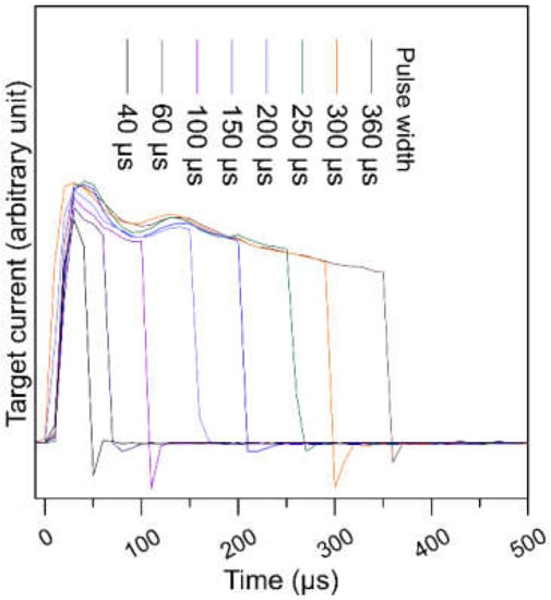
Figure 1.
The single current pulse shapes at square pulse voltage but different pulse width for discharges with a Cr target in argon at 0.8 Pa.
Several analyses were conducted to examine and to compare the properties of Cr coating deposited by different conditions. The top and cross-sectional microstructures of deposited films are observed by using a scanning electron microscope (SEM), (S-4800 Cold Field Emission Scanning Electron Microscope, Hitachi, Tokyo, Japan). Crystallinity of the films was characterized by utilizing a D8 Discover X-ray diffractometer (Bruker, Billerica, MA, USA) with a Cu Kα radiation.
Thicknesses of the thin films were measured by using a Calotest Compact Calotester (CAT²c, Anton Paar, Graz, Austria). Thickness calculations of the sample were based on the standard EN 1071-2 [20]. The radii of balls were maintained at 75 mm. Thicknesses at 3 locations of each sample were measured in order to calculate the average film thickness. A TTX-NH3 nanoindentation tester (Anton Paar, Graz, Austria) was used to estimate the hardness and elastic modulus of Cr coatings. The indentations were carried out using a maximum load of 2.5 mN with a 10 s pause. The average hardness of each coating was calculated from more than 16 indents.
During the trial runs, it was found that it was difficult to maintain the desired constant substrate bias voltage in a HiPIMS process. The substrate bias voltage dropped while the HiPIMS discharge initiates, as described in literature [8,13]. Moreover, the adhesion of these trial Cr coatings was not sufficient for the above mentioned mechanical tests. To overcome these issues, the synchronized substrate bias voltage and Cr ion bombardment were introduced. At the same time as the HiPIMS discharge began, the substrate bias voltage, at −1000 V, pulses with a pulse width of 1 ms, which was synchronously initiated for accelerating Cr ions to bombard on the substrate. With Cr ion bombardment for 10 min, a Cr interlayer was precoated onto the substrate and the substrate temperature increased to about 210 °C. The substrate bias voltage was then changed to 0 V (grounded) and −200 V immediately without any gradient substrate biasing, to deposit a subsequent Cr top-layer. The top-layer deposition time of the different parameters was adjusted to achieve a close total film thickness around 1.8 μm. The additional parameters for deposition of chromium films utilizing the synchronized substrate bias are listed in Table 2. After deposition, the substrate temperature might lower down to about 200 to 190 °C.
Table 2.
The additional parameters for the deposition of chromium coatings, utilizing synchronized substrate bias voltage pulses.
3. Results and Discussion
3.1. Effects of the Deposition Pressure and the HiPIMS Pulse Width on the Cr Film Structure
Figure 2 and Figure 3 show the top and cross-sectional SEM SE images of HiPIMS Cr films deposited at the same substrate bias of −30 V, but different deposition pressures, 0.8 and 1.2 Pa, and different pulse widths, 60, 200 and 360 μs, on silicon wafer chips. At such small and unstable substrate biasing, all six films present similar columnar cross-sectional features, which are in the range of Zone 1 according to the structure zone model proposed by Anders based on Thornton’s structure zone model [21]. Chromium films of pulse width 60 μs and deposition pressure 1.2 Pa exhibit an individual tetrahedron-top columns morphology, which is similar to chromium films deposited by a direct current or a radio frequency magnetron sputtering [6,18,22,23,24,25].
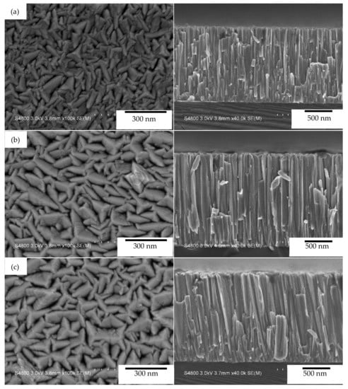
Figure 2.
Top (left side) and cross-sectional (right side) SE micrographs of Cr films deposited at the substrate bias of dc −30 V, the deposition pressure of 0.8 Pa, and the HiPIMS pulse width of (a) 60 μs, (b) 200 μs, and (c) 360 μs, on a silicon wafer.
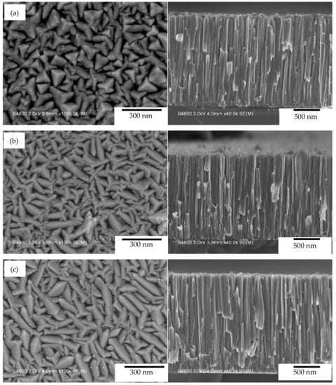
Figure 3.
Top (left side) and cross-sectional (right side) SE micrographs of Cr films deposited at the substrate bias of dc −30 V, the deposition pressure of 1.2 Pa, and the HiPIMS pulse width of (a) 60 μs, (b) 200 μs, and (c) 360 μs, on silicon wafer.
The morphology of the film of 60 μs and 0.8 Pa is more like 3-point star top columns. With elongating the pulse width or decreasing deposition pressure, the tetrahedron-top columns widen along the three ridges and become tangled 3-point star top columns. This phenomenon is also found in other reported HiPIMS Cr films deposited at modulate peak power [5,18]. In HiPIMS processes, both the numbers of ions and the portion of high energy ions increase with peak power [16], which enables a higher mobility of adatom to diffuse further [11,26]. Since the target voltage pulse waveform in this study is similar to the square pulse, the peak power can be considered in proportion to the pulse width. The X-ray diffraction patterns of deposited films also support this inference. The preferred orientation of Cr (110) reduces with elongating pulse width and decreasing deposition pressure. The deposition rate of 1.2 Pa is about 1% to 17% lower than that of 0.8 Pa, and the difference decreases with the pulse width. This could be attributed to the compromise between higher scattering loss of the Cr species during the flight and higher sputtering rate of the target at high working pressure. The collision which occurs between sputtered Cr ions and other species may reduce the kinetic energy and change the flight path of the Cr species, which subsequently decreases the flux of the Cr species toward the substrate. On the other hand, high working pressure causes a higher sputtering rate of the target and more easily initiates the self-sputtering dominate phase in each pulse, and the proportion of self-sputtered species increases with the pulse width [9]. All these factors play important roles in the deposition rate of the HiPIMS process.
To compare the difference of incident ions to substrate at different deposition pressure and different pulse widths, the responded substrate current pulses are recorded during the Cr ion bombardment stage by utilizing the built-in oscilloscope of the bias power supply. As shown in Figure 4, the substrate peak current increases with the target pulse width. This indicates that the ion number and ion charge increase with the pulse width. However, the contributions of Ar or Cr ions remain indistinguishable from the substrate current. All the substrate current pulse widths are broader than the target current pulse width in Figure 1. However, the maximum substrate current occurred at 180 μs which is 140 μs later than when the maximum target current occurred at 40 μs in Figure 1. This delay could be attributed to the durations of the ion recycling, the transformation from gas sputtering into self-sputtering in HiPIMS discharge [8,9,15], and the flight of ions from target to substrate. In the initial stage of HiPIMS discharge, the strong negative voltage on the target attracts back a large fraction of the gas ions and sputtered metal ions, which limits the fraction of ions that reach the substrate, until the conditions for the discharge current runaway are fulfilled [8,9]. No significant delay between pulses of 0.8 and 1.2 Pa was found, but the pulses of 1.2 Pa seem to be 20 μs broader at the tail than those of 0.8 Pa. The broader substrate current pulses also indirectly support an argument that the flight path of ions would be changed by the pressure. The responded substrate current of pulse width 60 μs is much lower than those of pulse width 200 and 360 μs. This implies the ionization ratio for pulse width 60 μs could be much lower and results in similar microstructures as those of DC magnetron sputtered chromium films.
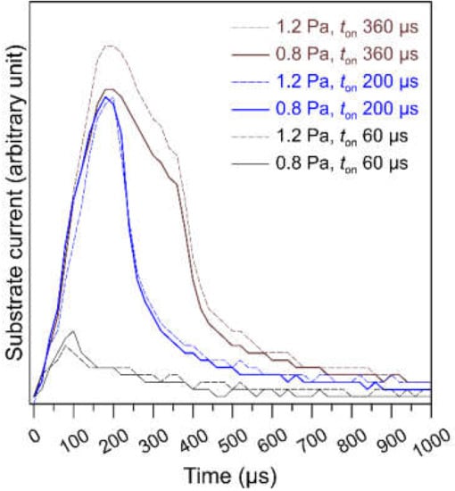
Figure 4.
The responded substrate bias current pulse shapes at a constant substrate bias pulse voltage of −1000 V for 1 ms which are synchronized with Cr target discharges of different HiPIMS pulse widths at different argon pressures.
Although it seems that using a pulse width of 360 μs is more beneficial in both deposition rate and ionization of sputtered species, using such a long pulse is usually accompanied by more arc discharge during the deposition and more sensitivity to the working pressure. Both situations are not propitious to film quality and to process stability. Since the films of pulse width 200 μs presented a similar structure and an approximate deposition rate the same as those of 360 μs, only pulse widths 60 and 200 μs were used in further experiments to investigate the influences of synchronized pulse substrate biasing.
3.2. Effects of Synchronized Pulse Substrate Bias and the HiPIMS Pulse Width on the Cr Film Structure
Figure 5 shows the cross-sectional scanning electron microscope SE images of Cr films deposited with different pulse widths and synchronized pulse substrate bias. It can be found that a 350 nm thick Cr interlayer was pre-deposited during the 10 min Cr ion bombardment. The interlayer presents a granular Zone 3 structure with a rough faceted top [21], which changes the structure of the following growth top-layer. In the Figure 5a, the film of pulse width 60 μs without substrate bias exhibits the same tetrahedron-top columns Zone 1 structure as those of dc −30 V substrate bias shown in Figure 2a and Figure 3a. However, the film of pulse width 200 μs without substrate bias is different from Figure 2b and Figure 3b. The rough interlayer top causes a domelike top columnar structure, which is in the range of Zone 1 to Zone T. Moreover, the edges of columns become less sharp as Figure 3b and Figure 5a. This again proves that the higher adatom mobility attributes to the larger portion of high energy ions with increased peak power. With −200 V synchronized pulse substrate bias voltage, both films of pulse width 60 and 200 μs present a same Zone 2 dense granular column structure as shown in Figure 5c,d. This reveals that applying −200 V substrate bias effectively enhances the kinetic energy of incident ions and subsequent mobility of adatoms, which can offset the disadvantage of a lower portion of high energy ions for short pulse widths. Nevertheless, the boundaries of columns in Figure 5d are not as clear as those in Figure 5c, just like the comparison between Figure 5a,b.
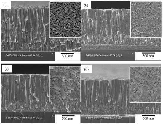
Figure 5.
Cross-sectional and top (right upper corner) SE micrographs of Cr films deposited at pressure of 0.8 Pa with (a) HiPIMS pulse width 60 μs/pulsed substrate bias 0 V; (b) HiPIMS pulse width 200 μs/pulsed substrate bias 0 V; (c) HiPIMS pulse width 60 μs/pulsed substrate bias −200 V; and (d) HiPIMS pulse width 200 μs/pulsed substrate bias −200 V.
The X-ray diffraction patterns of Cr films deposited at different HiPIMS pulse widths and pulsed substrate bias voltages are shown in Figure 6. There is a strongest peak Cr (110) in all four diffractograms. Without substrate biasing, the peak intensity of Cr (110) for the film of pulse width 200 μs is stronger than that of pulse width 60 μs. This indirectly proves that the higher mobility of adatoms may form a more crystalline structure when a longer pulse width is used. However, the second strongest peak is different in films of pulse width 60 and 200 μs. For films of pulse width 60 μs, applying substrate biasing enhances the peak intensity and causes a significant shift of Cr (211) to the lower 2θ value. Similar peak intensity enhancement and peak shifting occurred on Cr (200) for films of pulse width 200 μs. Similar changes of the preferred orientation have been found on titanium nitride films [11,26,27,28,29]. Applying longer pulses and substrate biasing increases the mobility of adatoms to migrate further on the planes, which requires longer diffusion distance [11,26]. In addition, higher kinetic energy of adatoms may also lead to an epitaxial growth of fine grain structure [27,28]. It can also be inferred that the high ion-to-atom ratio and high ion bombardment causes recrystallization and epitaxial growth of grains [29]. The peak shifting could be caused by the effects of ion bombardment. Since the peak position shifts to lower 2θ values, it usually indicates the formation of compressive stresses [18]. The preference of Cr (110), Cr (211), and Cr (200) is not clear. It is affected not only by the HiPIMS pulse width, but also by the deposition temperature and the deposition pressure [30].
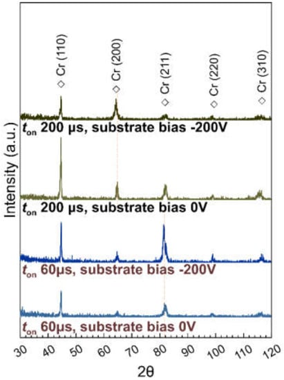
Figure 6.
X-ray diffraction (XRD) spectra of Cr films deposited at pressure of 0.8 Pa and 200 ± 10 °C with different HiPIMS pulse widths (ton) and pulsed substrate bias voltages.
Table 3 shows the nanoindentation result of Cr film deposited at different HiPIMS pulse widths and pulsed substrate bias voltages. The film of pulse width 60 μs and 0 V substrate bias is unable to be indented because of insufficient film adhesion. The hardness of pulse width 200 μs is much higher than that of pulse width 60 μs. It is consistent with the reported trend that Cr film hardness increases with the peak power [18]. The increased hardness for films deposited with longer pulse width could be attributed to the elimination of inter-columnar voids which result from the shadowing effect [31]. This is supported by the blurring of column boundary in Figure 5. However, in this study, applying substrate biasing did not enhance the film hardness as reported in reference [18]. This could be due to the Hall–Petch effect from grown grain size which countervails the benefit from increased film density [31,32].
Table 3.
Comparison of nanoindentation hardness of Cr films deposited by using different HiPIMS pulse widths and substrate bias voltages.
4. Conclusions
This research focuses on the effects of discharge pulse width on chromium films deposited by using high power impulse magnetron sputtering. With the conditions of same average power and pulse duty cycle, the microstructure of Cr films deposited at different working pressure, voltage pulse width, and substrate biasing were compared.
The deposition rate of Cr thin film at working 0.8 Pa is slightly higher than at 1.2 Pa. Furthermore, the difference of deposition rate between the two pressures decreases with the discharge pulse width. The deposition rate of short pulse width 60 μs is lowest, but those of 200 μs, and 360 μs are approximate.
The microstructure of Cr films coated at short pulse width with no or small direct current substrate biasing is similar to the typical direct current or radio frequency magnetron sputtering deposited Cr films. The film structure changes from individual prism-like columns into a tangled 3-point/4-point star columns morphology with elongating of the discharge pulse width. Applying synchronized substrate bias voltage is effective to alter the loose columnar film microstructure into a high crystalline dense film microstructure. Stronger synchronized substrate biasing and longer pulse width can enhance the ion flux toward the substrate, which changes the preferred orientation of Cr films from Cr (110) to Cr (200) and Cr (211), reduces the intercolumn void, and enables a higher film hardness.
Author Contributions
Conceptualization, C.-C.K. and J.-T.C.; data curation, C.-H.L.; funding acquisition, Y.-T.L.; investigation, C.-H.L.; methodology, C.-C.K. and J.-T.C.; project administration, C.-C.K.; resources, Y.-T.L.; supervision, C.-C.K.; visualization, J.-T.C.; writing–original draft, J.-T.C.; writing–review and editing, C.-C.K. All authors have read and agreed to the published version of the manuscript.
Funding
This research received no external funding.
Acknowledgments
The authors wish to thank Supati Cooperation for financial support. Precision Instrument Support Center of Feng Chia University and Micro-Nano Technology Lab of National Formosa University are also acknowledged for the microstructure analysis instruments.
Conflicts of Interest
The authors declare no conflict of interest.
References
- Bikulčius, G.; Češunienė, A.; Selskienė, A.; Pakštas, V.; Matijošius, T. Dry sliding tribological behavior of Cr coatings electrodeposited in trivalent chromium sulphate baths. Surf. Coat. Technol. 2017, 315, 130–138. [Google Scholar] [CrossRef]
- Daure, J.L.; Carrington, M.J.; Shipway, P.H.; McCartney, D.G.; Stewart, D.A. A comparison of the galling wear behaviour of PVD Cr and electroplated hard Cr thin films. Surf. Coat. Technol. 2018, 350, 40–47. [Google Scholar] [CrossRef]
- Navinšek, B.; Panjan, P.; Milošev, I. PVD coatings as an environmentally clean alternative to electroplating and electroless processes. Surf. Coat. Technol. 1999, 116, 476–487. [Google Scholar] [CrossRef]
- Vergason, G.; Fitch, M.; Smith, R.; Brazil, M.; Jochum, T. PVD chromium coatings replacing decorative chromium electroplated coatings on plastics. In Proceedings of the 58th Annual Technical Conference Proceedings, Santa Clara, CA, USA, 25–30 April 2015. [Google Scholar] [CrossRef]
- Li, B.; Gali, O.A.A.; Shafiei, M.M.; Hunter, J.A.; Riahi, A.R. Aluminum transfer buildup on PVD coated work rolls during thermomechanical processing. Surf. Coat. Technol. 2016, 308, 244–255. [Google Scholar] [CrossRef]
- Merij, A.C.; Sugahara, T.; Martins, G.V.; Sobrinho, A.S.D.; Reis, D.A.P.; Goncalves, P.A.R.; Massi, M. Use of Cr interlayer to promote the adhesion of SiC films deposited on Ti–6Al–4V by HiPIMS. Mater. Res. 2015, 18, 904–907. [Google Scholar] [CrossRef]
- Lattemann, M.; Ehiasarian, A.P.; Bohlmark, J.; Persson, P.Å.O.; Helmersson, U. Investigation of high power impulse magnetron sputtering pretreated interfaces for adhesion enhancement of hard coatings on steel. Surf. Coat. Technol. 2006, 200, 6495–6499. [Google Scholar] [CrossRef]
- Lundin, D.; Minea, T.; Gudmundsson, J.T. High Power Impulse Magnetron Sputtering: Fundamentals, Technologies, Challenges and Applications; Elsevier: Amsterdam, The Netherlands, 2019; ISBN 9780128124543. [Google Scholar]
- Anders, A. Tutorial: Reactive high power impulse magnetron sputtering (R-HiPIMS). J. Appl. Phys. 2017, 121, 171101. [Google Scholar] [CrossRef]
- Kouznetsov, V.; Macak, K.; Schneider, J.; Helmersson, U.; Petrov, I. Hybrid HIPIMS and DC magnetron sputtering deposition of TiN coatings: Deposition rate, structure and tribological properties. Surf. Coat. Technol. 1999, 12, 290. [Google Scholar] [CrossRef]
- Machunze, R.; Ehiasarian, A.; Tichelaar, F.; Janssen, G.; Ehiasarian, A. Stress and texture in HIPIMS TiN thin films. Thin Solid Films 2009, 518, 1561–1565. [Google Scholar] [CrossRef]
- Bugaev, S.P.; Sochugov, N.S. Production of large-area coatings on glasses and plastics. Surf. Coat. Technol. 2000, 131, 474–480. [Google Scholar] [CrossRef]
- Greczynski, G.; Lu, J.; Jensen, J.; Bolz, S.; Kölker, W.; Schiffers, C.; Lemmer, O.; Greene, J.E.; Hultman, L. A review of metal-ion-flux-controlled growth of metastable TiAlN by HIPIMS/DCMS co-sputtering. Surf. Coat. Technol. 2014, 257, 15–25. [Google Scholar] [CrossRef]
- Zuo, X.X.; Ke, P.P.; Chen, R.; Li, X.; Odén, M.; Wang, A. Discharge state transition and cathode fall thickness evolution during chromium HiPIMS discharge. Phys. Plasmas 2017, 24, 083507. [Google Scholar] [CrossRef]
- Anders, A.; Andersson, J.; Ehiasarian, A. High power impulse magnetron sputtering: Current-voltage-time characteristics indicate the onset of sustained self-sputtering. J. Appl. Phys. 2007, 102, 113303. [Google Scholar] [CrossRef]
- Greczynski, G.; Hultman, L. Time and energy resolved ion mass spectroscopy studies of the ion flux during high power pulsed magnetron sputtering of Cr in Ar and Ar/N2 atmospheres. Vacuum 2010, 84, 1159–1170. [Google Scholar] [CrossRef]
- Vetushka, A.; Ehiasarian, A.P. Plasma dynamic in chromium and titanium HIPIMS discharges. J. Phys. D Appl. Phys. 2008, 41, 015204. [Google Scholar] [CrossRef]
- Ferreira, F.; Serra, R.; Oliveira, J.C.; Cavaleiro, A. Effect of peak target power on the properties of Cr thin films sputtered by HiPIMS in deep oscillation magnetron sputtering (DOMS) mode. Surf. Coat. Technol. 2014, 258, 249–256. [Google Scholar] [CrossRef]
- Gudmundsson, J.T.; Alami, J.; Helmersson, U. Spatial and temporal behavior of the plasma parameters in a pulsed magnetron discharge. Surf. Coat. Technol. 2002, 161, 249–256. [Google Scholar] [CrossRef]
- Comite Europeen de Normalisation. Advanced Technical Ceramics—Methods of Test for Ceramic Coatings—Part 2: Determination of Coating Thickness by the Crater Grinding Method; EN 1071-2; Comite Europeen de Normalisation: Brussels, Belgium, 2002. [Google Scholar]
- Anders, A. A structure zone diagram including plasma-based deposition and ion etching. Thin Solid Films 2010, 518, 4087–4090. [Google Scholar] [CrossRef]
- Besnard, A.; Martin, N.; Millot, C.; Gavoille, J.; Salut, R. Effect of sputtering pressure on some properties of chromium thin films obliquely deposited. Mater. Sci. Eng. 2010, 12, 012015. [Google Scholar] [CrossRef]
- Wang, S.F.; Lin, H.C.; Bor, H.Y.; Tsai, Y.L.; Wei, C.N. Characterization of chromium thin films by sputter deposition. J. Alloys Compd. 2011, 509, 10110–10114. [Google Scholar] [CrossRef]
- Akbarnejad, E.; Soleimani, E.A.; Ghorannevis, Z. Chromium thin film deposition on ITO substrate by RF sputtering. J. Theor. Appl. Phys. 2014, 8, 129. [Google Scholar] [CrossRef]
- Kim, D.K.; Lee, K.S.; Yoon, Y.S. Effect of CrN barrier on fuel-clad chemical interaction. Nucl. Eng. Technol. 2018, 50, 724–730. [Google Scholar] [CrossRef]
- Gall, D.; Kodambaka, S.; Wall, M.A.; Petrov, I.; Greene, J.E. Pathways of atomistic processes on TiN (001) and (111) surfaces during film growth: An ab initio study. J. Appl. Phys. 2003, 93, 9086–9094. [Google Scholar] [CrossRef]
- Elmkhah, H.; Attarzadeh, F.; Fattah-alhosseini, A.; Kim, K.H. Microstructural and electrochemical comparison between TiN coatings deposited through HIPIMS and DCMS techniques. J. Alloy. Compd. 2018, 735, 422–429. [Google Scholar] [CrossRef]
- Alami, J.; Maric, Z.; Busch, H.; Klein, F.; Grabowy, U.; Kopnarski, M. Enhanced ionization sputtering: A concept for superior industrial coatings. Surf. Coat. Technol. 2014, 255, 43–51. [Google Scholar] [CrossRef]
- Mahieu, S.; Depla, D. Reactive sputter deposition of TiN layers: Modelling the growth by characterization of particle fluxes towards the substrate. J. Phys. D Appl. Phys. 2009, 42, 053002. [Google Scholar] [CrossRef]
- De Monteynard, A.; Schuster, F.; Billard, A.; Sanchette, F. Properties of chromium thin films deposited in a hollow cathode magnetron powered by pulsed DC or HiPIMS. Surf. Coat. Technol. 2017, 330, 241–248. [Google Scholar] [CrossRef]
- Greczynski, G.; Jensen, J.; Hultman, L. Mitigating the geometrical limitations of conventional sputtering by controlling the ion-to-neutral ratio during high power pulsed magnetron sputtering. Thin Solid Films 2011, 519, 6354–6361. [Google Scholar] [CrossRef]
- Lintymer, J.; Martin, N.; Chappé, J.-M.; Delobelle, P.; Takadoum, J. Nanoindentation of chromium zigzag thin films sputter deposited. Surf. Coat. Technol. 2005, 200, 269–272. [Google Scholar] [CrossRef]
© 2020 by the authors. Licensee MDPI, Basel, Switzerland. This article is an open access article distributed under the terms and conditions of the Creative Commons Attribution (CC BY) license (http://creativecommons.org/licenses/by/4.0/).