1. Introduction
On the surfaces of typical solar cells, antireflection films such as silicon nitride (Si
xN
y) films with randomly distributed pyramid-like structures are deposited on the
n+ layers to reduce the reflection of light intensity from the solar-cell surface. However, when busbar and finger electrodes are fabricated on the solar cells, the antireflection film should be removed from areas where the electrode deposition takes place because the film forms a barrier to electric power. Thus, electrode grooves are fabricated to remove the antireflection film from the electrode-forming layer of the cell [
1]. Moreover, improvement in the quantum efficiency of the charge carriers, and prevention of leakage current resulting from the destruction of the junction after electrode-fabrication processes such as Ni gilding, sintering, and Cu gilding can be achieved by applying a highly concentrated phosphorous-diffusion layer on the etched surface [
2,
3].
Nonequilibrium plasma generated at normal atmospheric pressure can be used to etch the electrode-groove pattern on an antireflection film. Plasma can be generated within an arbitrarily small region using surface-discharge plasma, so any groove pattern can be etched without masking the antireflection film. Herein, we propose the fabrication of antireflection films with etched electrode grooves on single crystalline silicon solar-cell substrates using surface-discharge plasma. The proposed technique is very economical because nonequilibrium plasma can be generated under normal atmospheric pressure without any masking material [
4,
5,
6,
7,
8].
Furthermore, from a practical viewpoint, thinner electrodes on grooves are desirable since they result in an active surface area for generating electricity. Therefore, we investigated the impact of the type of carrier gas on the etching profile formed using surface-discharge plasma. In addition to textures created using wet-film formation, the silicon solar-cell substrate is coated with an antireflection film, such as an Si
xN
y film, which complicates the determination of the impact of the type of carrier gas on the etching of the silicon solar-cell substrate [
9,
10].
In this study, electrode grooves were formed by etching antireflection films using surface-discharge plasma under Ar/CF4 and He/CF4 gases. Furthermore, we investigated and compared the etching characteristics on the basis of differences in the widths of the electrode grooves etched on the SixNy film.
2. Experiment Methods
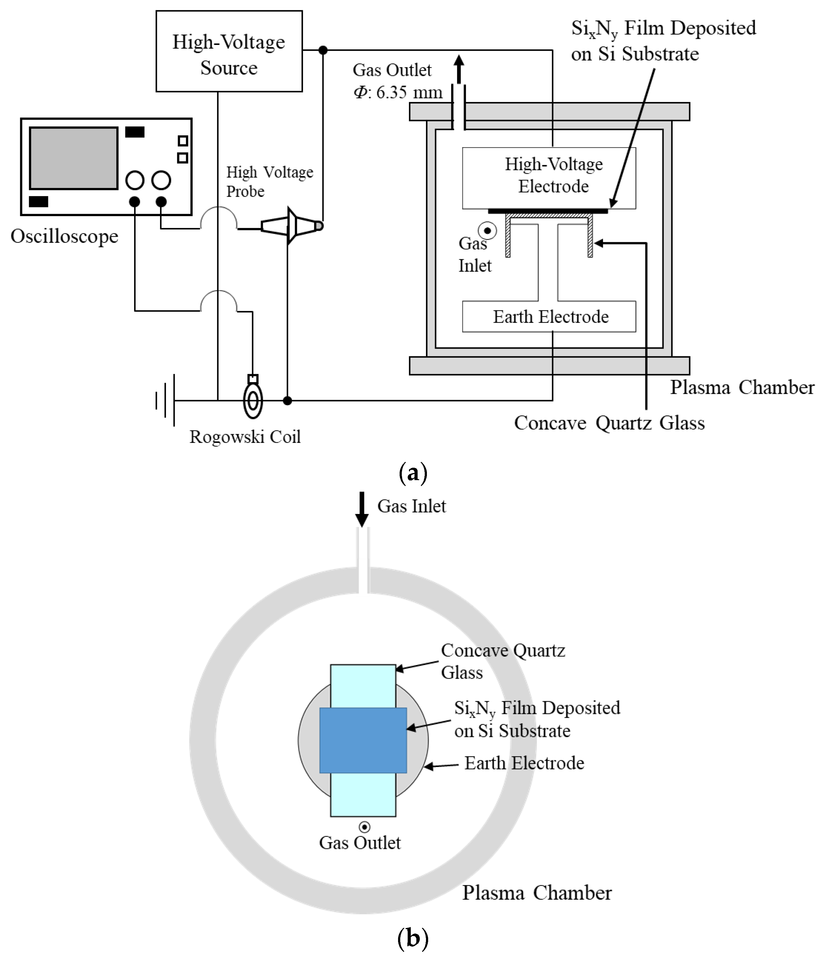
Figure 1 shows a schematic of the etching system used in this experiment. Surface discharge was induced by the arrangement of a metallic electrode whose side was covered with a quartz-glass layer with a 30 mm wide, 70 mm long, and 15 mm high concave part. The thickness of the quartz-glass layer of the convex part was 1 mm. A crystalline silicon substrate with one side of the surface covered with a 150 nm thick silicon nitride (Si
xN
y) film was sandwiched by the convex part and a cylindrical metal electrode with 70 mm diameter (chamfered edge:
R = 3 mm). The surface of the Si
xN
y faced the concave quartz-glass electrode. We used a p-type single crystalline silicon substrate prepared using the Czochralski method (BPSolar, Madrid, Spain) with dimensions of 125 mm × 125 mm, and thickness and resistivity of 0.27 mm and 2–4 Ω·cm, respectively. For the experiments, 40 mm × 30 mm specimens were cut. Using low-pressure plasma chemical-vapor deposition, a Si
xN
y film with a refractive index of approximately 2.4 was deposited on the surface of a silicon substrate textured by wet chemical etching. Carrier gases (Ar and He) and CF
4 controlled by mass-flow controllers (SFC-280E, Hitachi Metals, Ltd., Tokyo, Japan, maximal flow rate was 3000 sccm) were supplied to the discharge area. For the Ar/CF
4 and He/CF
4 mixture gases, the residual air in a cylindrical discharge vessel with an inner diameter of 135 mm and a height of 175 mm was exhausted up to 50 Pa, after which a mixed gas composed of the carrier gas (Ar or He) and CF
4 was filled up at atmospheric pressure. Subsequently, the residual gas was exhausted by performing inlet and exhaust of gas at a total gas flow rate of 1000 sccm for 5 min. With the surface-discharge plasma generated under the above conditions, the nitrogen spectrum in the residual air was not observed in the emission spectroscopic measurement taken with a spectroscope (USB-4000, Ocean Optics, Inc., Douglas Avenue Dunedin, FL, USA), as shown in
Figure 2, which is described later. A mixed gas composed of the carrier gas and CF
4 was introduced from the side of the discharge vessel, and exhausted from the exhaust port provided on the upper surface of the discharge vessel. The height of the gas inlet was the same as the height of the area where the surface discharge was generated. High voltage with a frequency of 9 kHz (Logy Electric Co., Tokyo, Japan, LTD., LHV-10AC, maximal peak-to-peak voltage (
Vpp) was 10 kV) was supplied to the upper electrode. Discharge voltage and current were observed with a high-voltage probe and a Rogowski coil, respectively. Si
xN
y film grooves were etched on single crystalline silicon substrates for various
Vd at atmospheric pressure; thereafter, we observed the width of the grooves using a microscope with a magnification of 50×. The plasma-etched silicon substrates were observed by scanning electron microscopy (SEM, JSM-7600F, JEOL Ltd., Tokyo, Janan).
3. Experiment Results
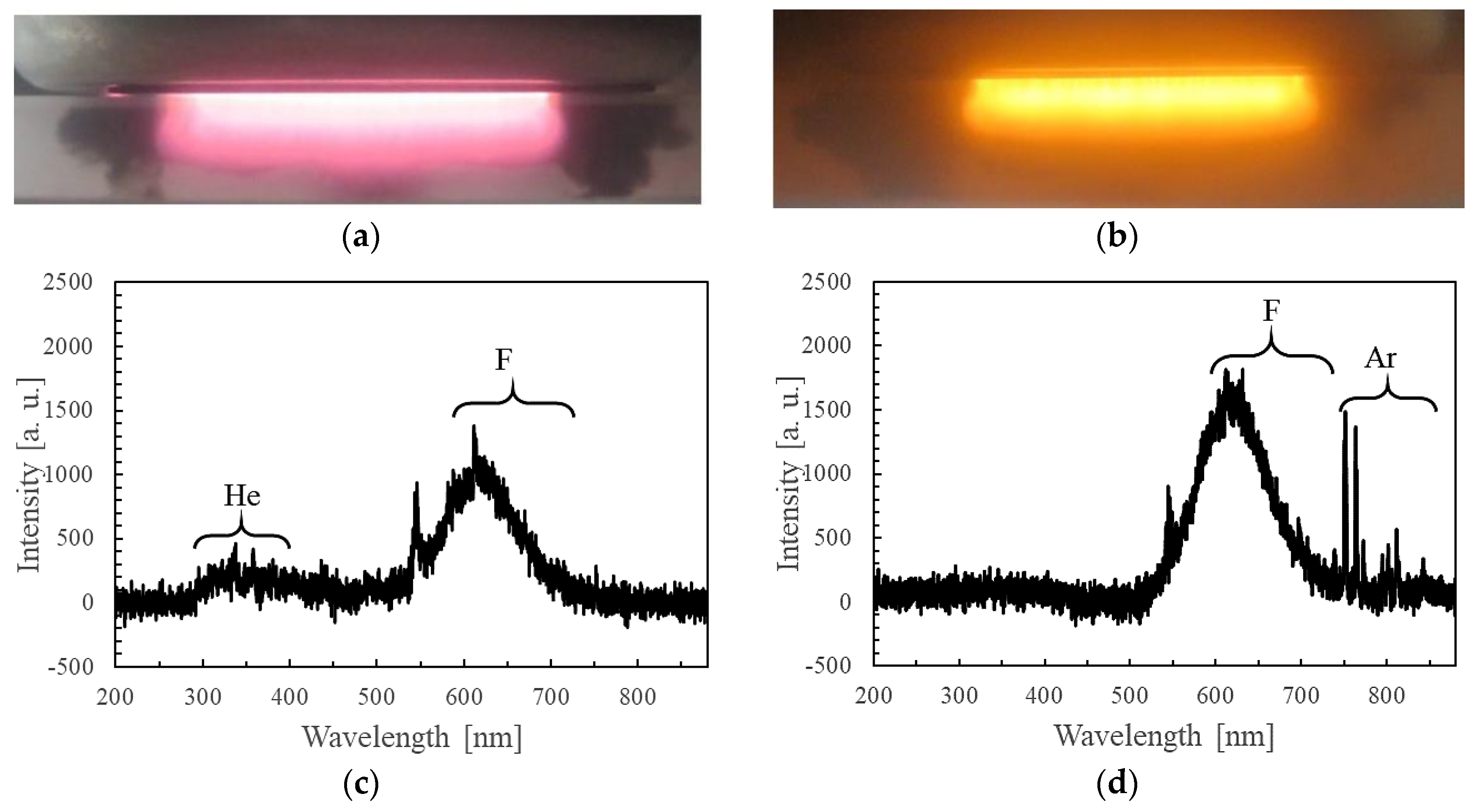
Figure 2 shows photographs of the surface-discharge plasma generated when the ratio of gas-flow rates was (
Figure 2a,c) Ar:CF
4 = 700:300 sccm and (
Figure 2b,d) He:CF
4 = 700:300 sccm, and the self-sustaining discharge voltage (
Vpp) was 9.4 kV. From
Figure 2, it can be seen that the surface-discharge plasma produced along the side of the concave dielectric body in this experiment contained intensely luminous surface streamers.
Figure 2c,d shows the emission spectra of the surface-discharge plasma under Ar/CF
4 and He/CF
4 conditions observed by multichannel spectroscopy (USB-4000, Ocean Optics Inc., Douglas Avenue Dunedin, FL, USA; wavelength range, 200–1100 nm; wavelength resolution, 1.5 nm) in a previous study [
11]. Some typical spectral lines could be observed in the emission spectra: fluorine (F) atoms at 600–750 nm; He atoms at 300–400 nm; Ar atoms at 750–880 nm [
11,
12]. The emission spectrum of CF
n is generally observed at 220–340 nm; however, emission intensity was too weak to measure [
1]. Nevertheless, the F peak was observed, so it could be inferred that CF
n was generated by dissociation of CF
4 in the plasma.
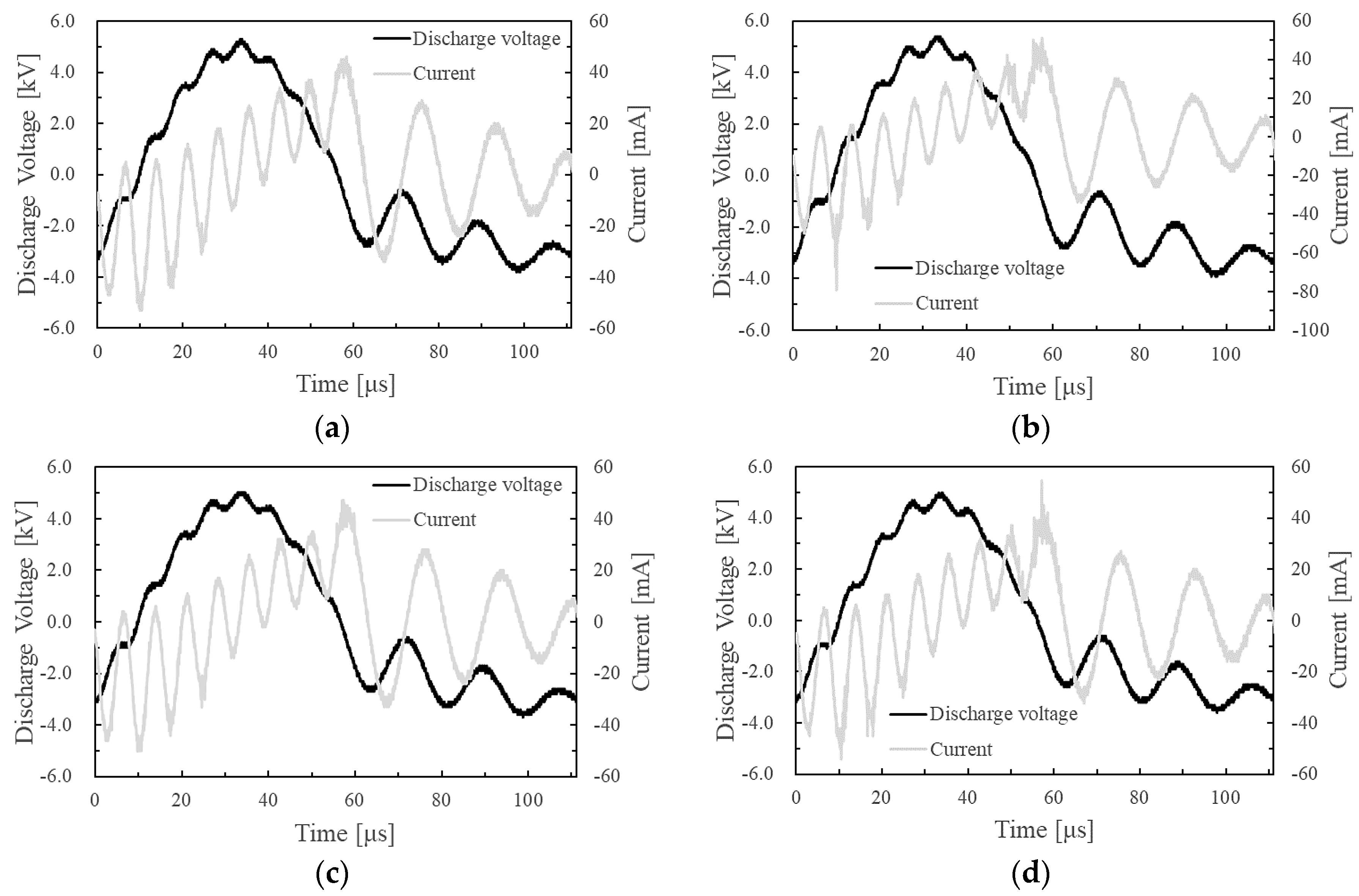
Figure 3 shows the corresponding discharge voltage and current waveforms. The discharge current was the pulsed current with a pulse duration of several ns generated by the surface-discharge plasma and displacement current owing to the dielectric body’s electrostatic capacitance. The discharge current consisted of a displacement current induced by the capacitance of an electrode system and microdischarge currents with pulse durations of several ns. The microdischarge was automatically terminated within a very short time by the electric field induced by charges accumulated on the dielectric materials, and thermal equilibrium could not be achieved. Thus, the gas temperature of the surface-discharge plasma was approximately between 300 and 500 K [
13]. The discharge power obtained by the integration of the discharge voltage and discharge current, shown in
Figure 3, for a period of discharge current and voltage, was about 9.07 and 8.33 W for the Ar/CF
4 and He/CF
4 gas mixtures, respectively.
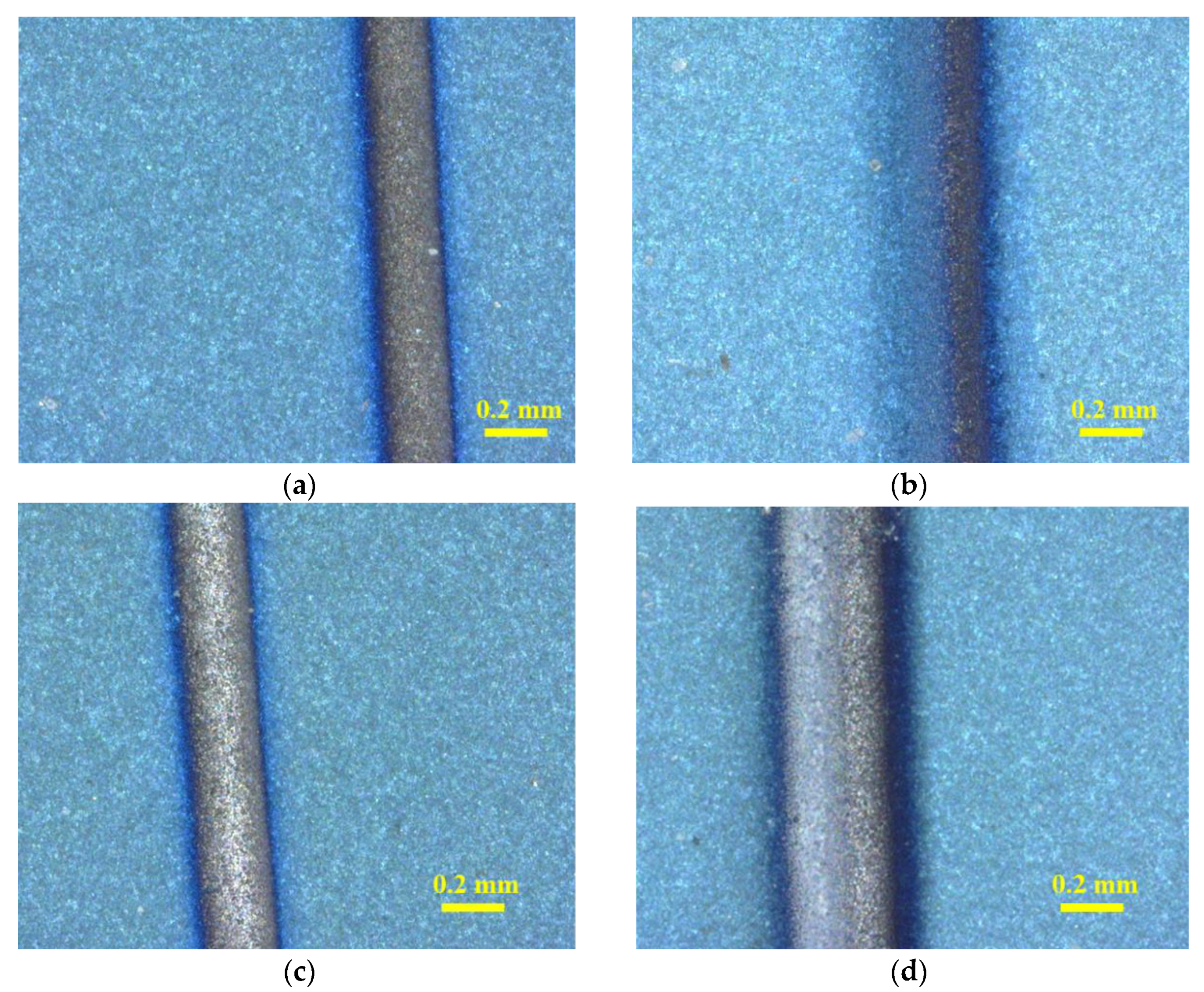
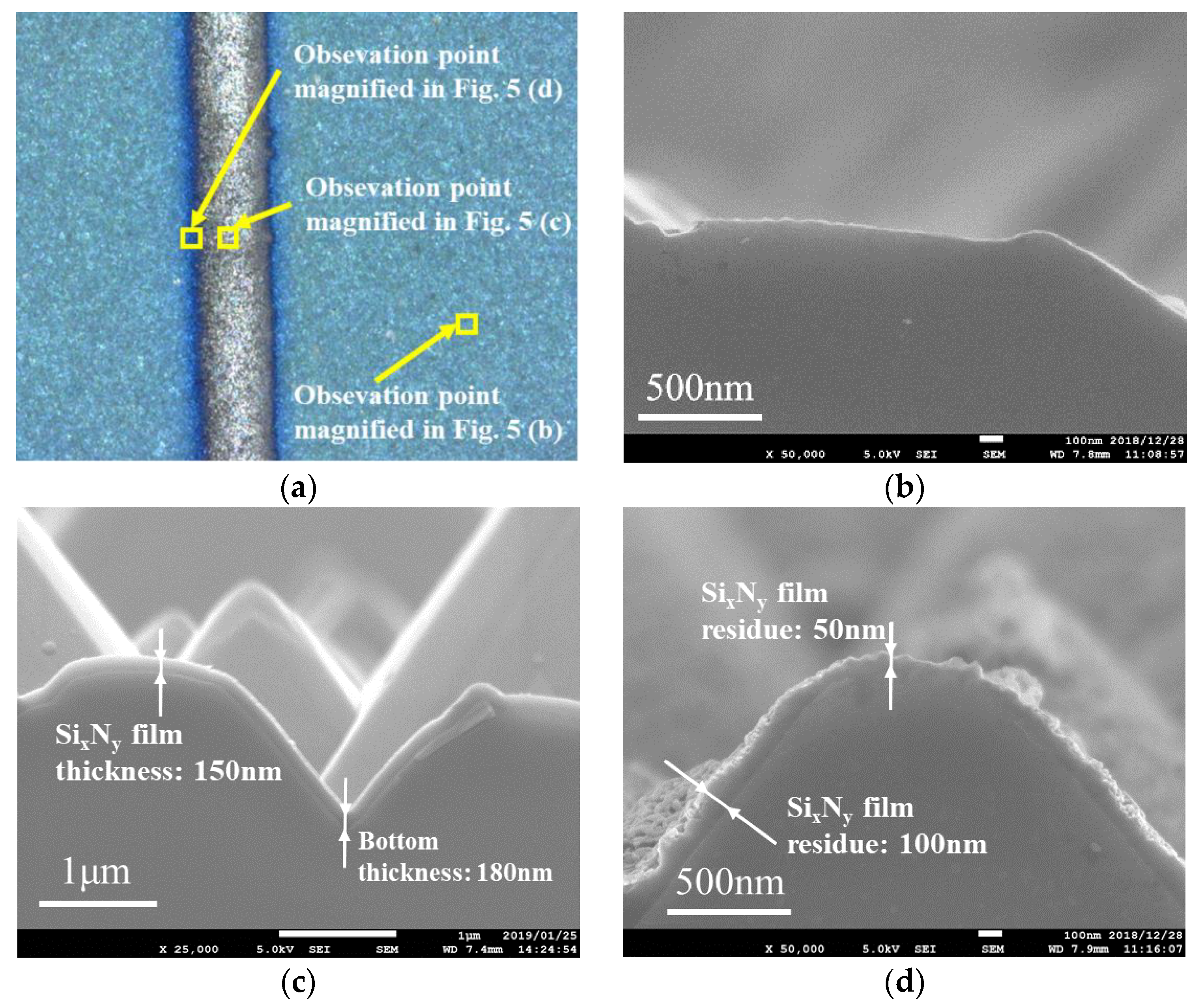
Figure 4 shows images of the silicon solar-cell substrate surfaces after etching. The flow rate of the carrier gas (Ar or He) and CF
4 was 700 and 300 sccm, respectively;
Vpp was 9.8 kV; plasma etching time (
te) with carrier gas (Ar or He) and CF
4 was 120 and 180 s, respectively. Linear electrode grooves were formed using the surface-discharge plasma generated along the side of the concave dielectric body. It was reported that, as the density of the surface-discharge plasma increases toward the center of the columnar surface streamer, Si
xN
y etching speed increases [
6]. Therefore, a region is formed at the edge of the electrode groove from which Si
xN
y cannot be removed.
Figure 5 shows SEM images of the silicon solar-cell substrate’s cross-section after etching. The parameters for the etching process were set as follows: Ar:CF
4 = 700:300 sccm,
Vpp = 9.8 kV, and
te = 180 s. We observed the cross-sections in the center and edge of the etched groove. From
Figure 5b, it can be seen that the Si
xN
y film deposited in the center of the groove was completely removed after etching, while, as can be seen from
Figure 5d, some parts of the film at the edge of the groove were not removed; in particular, film residues were observed along the bottom of the pyramid-shaped textures. As shown in
Figure 5c, although the higher thickness of the Si
xN
y film at the bottom of the pyramid-shaped texture than at the top is one of the main reasons for the presence of the film residues along the bottom, another reason may be the difference in the etching speed of the Si
xN
y film between the top and bottom of the texture. Because the electric-field strength at the top of the texture was higher than that at the bottom of the texture, the etching effect caused by the ions affected by the electric field was higher at the top of the texture.
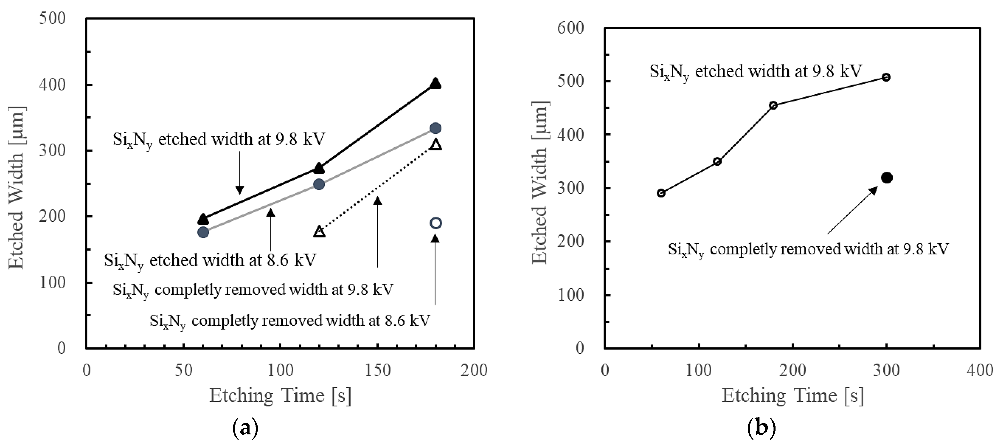
Figure 6a,b shows the relationship between groove width and discharge voltage, and between groove width and etching time, respectively, with either Ar or He. The width of the groove was determined from the cross-sectional images shown in
Figure 5b,d. To define the etching width, we measured both the region from which the Si
xN
y film was completely removed and the region in which film residues were observed.
Figure 6 shows that width increased as applied voltage and etching time increased. With time
te, etching progressed via ions and radical species generated in the plasma area. Thus, when the applied voltage was high, the generation of ions and radical species that contributed to the etching of the plasma became more active, and etching rate increased. Higher applied voltages produced more activated species, such as F
x and CF
3, and other reaction intermediates that contributed to the etching. Etching with surface-discharge plasma created columnar surface streamers with diameters as large as 200 μm. Both plasma density and etching speed were highest at the center of the plasma region, and etching speed was reduced toward the edge, thereby widening the region across which the Si
xN
y film was removed with increasing etching time.
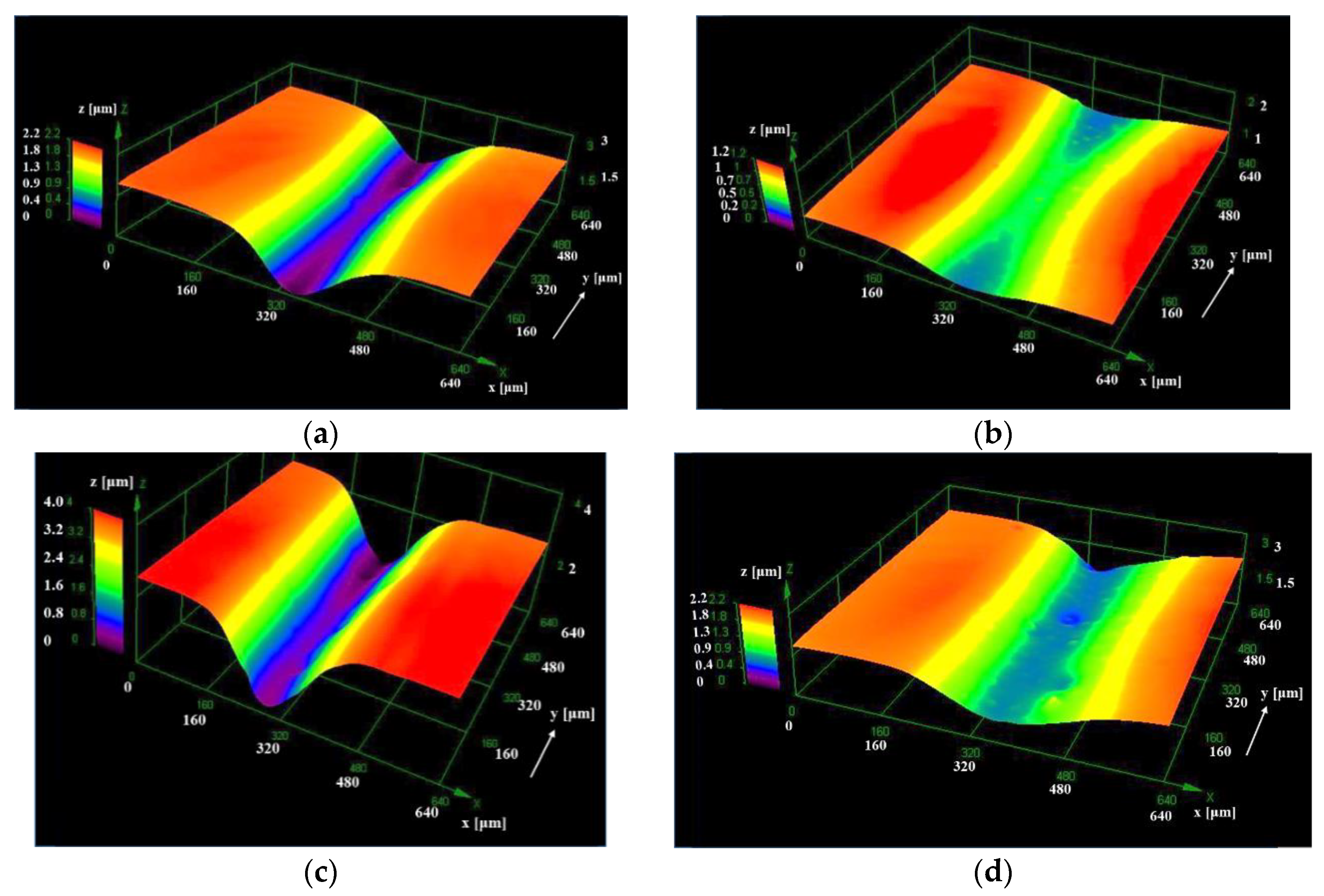
Figure 7 shows the 3D profiles of the groove (as shown in
Figure 8) prepared with He and Ar as carrier gasses at
Vpp = 9.8 kV and
te = 5 and 10 min. In
Figure 7, the surface condition of the silicon substrate was flat, and the Si
xN
y film was not coated. Therefore, we investigated the progress of silicon etching due to surface-discharge plasma.
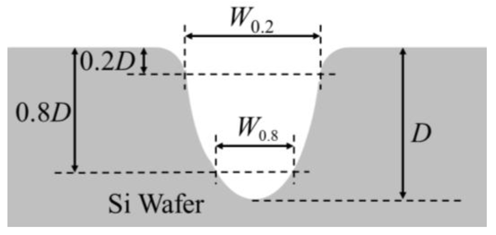
Table 1 shows groove depths
D and the groove widths at 0.8 and 0.2
D, obtained from
Figure 6. The reported width and depth of the grooves were average values of the 3D etched profile. In
Figure 7, the progress was not only in the depth direction, but also in the width direction as time passed. Etching along the horizontal direction outside the streamer diameter progressed via diffusion of the radical species, and was independent of the electric field; consequently, the progression of etching in the horizontal width direction was slow.
4. Discussion
From
Table 1, it can be seen that the widths of electrode grooves etched using He were clearly wider than those etched using Ar. When He, which is lighter and more susceptible to diffusion than Ar, is used as the carrier gas, the plasma generated along the side of the dielectric body is transient glow discharge that extends over a wide region and widens the electrode groove. As shown in
Figure 6a,b, the Si
xN
y film was completely removed across some of the groove width when the groove was etched for
te > 120 s at
Vpp = 9.8 kV in an Ar/CF
4 gas atmosphere; however, when the groove was etched for the same duration in a He/CF
4 gas atmosphere, the Si
xN
y film was not removed across the entire width. In He/CF
4 gas atmosphere and
Vpp = 9.8 kV,
te > 300 s was required for the complete removal of the Si
xN
y film. This demonstrated that the etching speed achieved using Ar as the carrier gas was higher than that achieved using He. This can be attributed to the ion-assisted etching caused by Ar ion bombardment. Although He
+ can be expected to have the same effect as Ar
+ because the ion bombardment energy obtained from Ar
+, which has a higher mass, is higher, the etching rate when using Ar as the carrier gas is higher than that when using He. The etching of Si
xN
y by the surface-discharge plasma performed in this study is an ion-assisted etching process using active species such as F
x and CF
n, and Ar
+ or He
+. To determine whether the etching effect of the active species or ion bombardment is dominant, the density of ions generated in the plasma and the density of active species have to be determined, which is beyond the scope of this study.
In the proposed process for generating the surface-discharge plasma, discharge was initiated at the triple junction between dielectric body, upper electrode (i.e., the Si substrate), and gases, which corresponded to the Paschen minimal point. The surface-discharge plasma developed along the side of the dielectric body that had higher electrical potential than the surrounding gas atmosphere. The surface-discharge plasma was columnar, and the dielectric body was generated by the rectangular dielectric electrode. Further, etching was also considered to be affected by the edge effect due to the bending of the electric-field line at the dielectric edge. This accounts for the width of the columnar surface streamer being directly related to the etching width. It is well known that He gas can generate an effective and stable atmospheric-pressure glow discharge with good spatial uniformity [
14]. Therefore, when He was used as the carrier gas, the range of the surface discharge expanded, and the horizontal etching width increased compared to when Ar was used. In contrast, when Ar was used as the carrier gas, the plasma range became localized, and the etching rate in the plasma range increased. In addition, Ar
+ ions generated in surface streamers were expected to facilitate etching, resulting in the progression of etching along the vertical depth direction.


