Abstract
Thin films of ZnO:Ga2O3 (ZGO) were deposited by radio frequency (RF) sputtering at voltages of 0.5, 0.9 and 1.1 kV. The films were studied with respect to their suitability in flexible piezoelectric nanogenerators. The analysis of the spectroscopic and microscopic results showed that piezoelectric features were revealed for the films grown at all sputtering voltages, but the most favorable morphology in terms of low roughness was achieved at 1.1 kV. The effect of the sputtering voltage on the films crystallinity and lattice strain was studied. It was found that the increasing sputtering voltage promoted the films crystallization. Additionally, the presence of oxygen vacancies in the piezoelectric films was negligible as it is not a major factor affecting their performance. The electrical measurements of the Ag/ZnO:Ga2O3/Ag harvester on a flexible substrate in the low-frequency range showed a piezoelectric voltage of 414 mV, a current of 10.4 µA and an electric power output of 1.4 µW at a mass load of 100 g. These results were achieved by a simple architecture of a single piezoelectric layer with a relatively small size of 3 cm2 and small piezoelectric film thickness (600 nm) containing lead-free material. It was proven that the sputtered ZGO films are suitable for energy harvesting elements and their performance could be tuned by the sputtering voltage. Another possible application of the proposed device, excluding low-frequency vibrational harvesting, could be a pressure sensor or strain gauge, due to the good linearity of the electrical parameter dependences on the strain.
1. Introduction
In recent years, piezoelectric energy harvesting devices have put the focus on the study of piezoelectric lead-free oxides as environmentally friendly materials [1,2,3]. ZnO films, with their good piezoelectric properties and their possibility of being produced by conventional deposition technologies, have become preferable lead-free materials for piezoelectric micro- and nanoelectromechanical (MEMS and NEMS) sensors, actuators, and energy harvesting devices [4,5]. However, making the devices smaller, more compact and the films thinner, a piezoelectric material with greater lattice asymmetry is needed to compensate dipole quenching due to the short distance between the opposite charges. Therefore, doped ZnO has to be a suitable material, close to ZnO in nature, but with enhanced piezoelectric properties. A variety of dopants have been found appropriate to keep the piezoelectric features of ZnO and, at the same time, to improve the conductivity due to constituents in their composition, such as Al2O3 and Ga2O3 [6,7]. Among them ZnO:Ga2O3 (ZGO) is preferable due to lack of diffusion or the migration of gallium, as compared to the aluminum or to the neighboring zones or interfaces. This is a desirable property for well-defined piezoelectric behavior, especially in thin film energy harvesting, where short circuits can occur due to the short path of the particles between the opposite electrodes [8]. With the development of the energy harvesting market, ZGO films are necessary to be implemented in flexible nanogenerator devices, requiring cyclic applied continuous mechanical loading with low frequency. However, the available studies reveal data mostly about the material conductivity and optical and gas sensing properties of ZGO and less about the piezoelectric response and its dimensions in sputtering growth conditions [9,10]. In fact, the sputtering conditions influencing the roughness, have a great effect on the piezoelectric device’s electrical contact, although the nanometric scale of the roughness [11]. Although the average film roughness is less than 2 nm, or less than 13% of the film thickness, the entire surface cannot get effectively into contact, resulting in a contact resistance variation between 80 and 200 mΩ [12]. The limitation of the current flow through smaller contact spots and the increase in the energy losses over the contact resistance has been further proven [13]. Thus, surface smoothness becomes one of the crucial conditions to guarantee the high performance of the piezoelectric energy harvesters.
Our group has recently developed and investigated a simple generator with sputtered ZGO on polymer seed layer and it has been established the optimal deposition conditions for obtaining uniform films with controllable thickness, but the structures have only been studied by impedance spectroscopy and dielectric characterization until now [14]. Some of the well-studied properties of ZGO films and composites are permittivity and leakage, related to energy storage applications [15], or leakage current and residual voltage for varistors [16]. The literature data for ZGO deposited by sputtering exhibit a great degree of variation in the reported properties—optical, gas sensing, strain sensing, etc. Thus, it has been important to determine the degree to which the films’ microstructures, chemical compositions and surface morphologies affect the piezoelectric device properties in terms of energy harvesting applications.
In this study, the relations between the ZGO films’ microstructures, functional groups, electronic states of elements and surface morphologies, the voltage generation abilities, and the produced power are investigated with respect to the sputtering voltage. The results showed that the gallium-doped zinc oxide films not only exhibited good piezoelectric properties but also that these properties can be tailored by the sputtering voltage. In this way, it was possible to produce comparable power density to other reported piezoelectric harvesters, involving lead-free materials, by using a similar design, but a smaller size of the converting element. However, to the best of the authors’ knowledge to this day, similar research studies have not been carried out or published.
2. Materials and Methods
The ZnO:Ga2O3 thin films were deposited on silicon substrates (purchased from Sil’Tronix ST, Archamps, France) for the needs of the spectroscopic measurements by radio frequency (RF) sputtering, using a 99.998% pure composite target ZnO/Ga2O3 = 95/5 wt.% (purchased from K. Lesker, East Sussex, UK). This was necessary to avoid the contribution of the polymeric substrate features appearing in the spectroscopic data and disturbing the signal being interpreted. For the mechanical testing, thermal resistant flexible substrates of polyethylene naphthalate (PEN) were used (purchased from Goodfellow, Cambridge, UK).
Before sputtering, the silicon substrates were cleaned. The standard procedure of silicon wafer cleaning for stripping the native SiO2 included dipping the wafers in 10% concentrated aqueous solution of hydrofluoric acid for 10 s. It is widely used in the industry because it was proven that, at such time and concentration of treatment, only the SiO2 film with angstrom thickness is removed, without affecting the surface roughness of the polished wafers [17]. Then, the Si wafers were treated using an ultrasonic bath in acetone, ethyl alcohol, and distilled water for 6 min. PEN substrates were cleaned by sonication in acetone for 180 s. For the generated piezoelectric voltage and current measurements, silver thin films were grown as a bottom electrode by thermal evaporation. The chamber for sputtering was evacuated to a vacuum level of 10−6 Torr. The specific deposition conditions were as follow: sputtering pressure was 2.5 × 10⁻² Torr; various plasma voltages in the range 0.5–1.1 kV were set and the plasma current values were between 80 and 140 mA (sputtering power ranged approximately between 40 and 154 W), defining the sputtering rates of 8–15 nm/min, respectively. The three samples deposited at different sputtering voltages are characterized with different film thicknesses due to the different sputtering rates. The same deposition conditions were used for the growth of the ZGO films on the two types of substrates. The top electrodes were also prepared by the thermal evaporation of silver and were segmented by a shadowing mask at 0.9 A per 10 s. Three segments, each with dimensions of 1.5 cm × 2.0 cm, were obtained on the top, thus defining the active piezoelectric areas.
The film thicknesses were measured by Tencor 200 Alpha Step profilometer (KLA-Tencor, CA, USA) in the range between 400 and 600 nm, according to the sputtering voltage applied between 0.5 and 1.1 kV, respectively. The identification of the chemical bonds and functional groups was performed by Fourier-transform infrared spectroscopy (FTIR) in transmission mode. FTIR spectra were recorded by a Shimadzu spectrophotometer IRPrestige-21 (Shimadzu Corporation, Kyoto, Japan). Atomic force microscopy (AFM) was conducted by AFM microscope MFP-3D Oxford Instruments (Oxford Instruments, Abingdon, UK) in non-contact mode. X-Ray Diffraction (XRD Philips 1710, Philips, Eindhoven, The Netherlands) was used to determine the crystalline features of the films. Scanning electron microscopy was conducted by SEM microscope Philips 515 (Philips, Eindhoven, The Netherlands). The electronic state analysis of the ZGO films was conducted by carrying out X-ray photoelectron spectroscopy (XPS), using an Omicron Multiprobe system (Omicron Nanotechnologies, Taunusstein, Germany) consisting of a monochromatic X-ray source (Al Kα) and a hemispherical electron analyzer (Omicron SPHERA, Omicron Nanotechnologies). The base pressure was 1.10−10 mbar. The XPS experiments were performed using the monochromatic X-ray source XM1000 and the SPHERA hemispheric analyzer from Omicron Nanotechnologies. The energy was calibrated to the peak position of the Au (111) 4f7/2 (binding energy of 83.9 eV) line. The samples were analyzed as-deposited (i.e. without any cleaning), and then Ar sputtering by 2.2 keV Ar+ ions at a pressure of 3 × 10⁻⁸ mbar was performed for 20 and 40 min. The spectra data were processed and analyzed using the CasaXPS program (Version 2.3.14). The mechanical load was applied from a laboratory-made shaking setup by mounting on a trapezoidal beam for the uniform distribution of the dynamic stress along the whole sample independently of its area. Vibrations with frequencies up to 50 Hz and intensities of up to 35 N (~9 N/cm2) were applied. Details about the mechanical test system and the way of sample mounting are provided elsewhere [18]. Oscillograms were recorded with digital oscilloscope Tektronix TDS 1012B (Tektronix, Berkshire, UK) and the current through the samples was measured by high-resolution picoamperemeter Keithley 6485 (Keithley Instruments, Berkshire, UK). All electrical measurements for the determination of the intrinsic properties of the harvester (assigned to the materials and films interfaces involved) were conducted at room temperature without load resistance.
3. Results and Discussion
FTIR spectra were recorded for the ZGO films, sputtered at different conditions, as shown in Figure 1a. The observed characteristic bands and their assignments are described in detail in Table 1. The weak absorption bands appeared at 2358.7 and 2329.7 cm−1 (not shown) and were ascribed to CO2 vibrations due to atmospheric air [19]. The significant characteristic bands were found in the range 350–750 cm−1, therefore, the FTIR results were extracted with a focus in this range. It should be noted that some typical absorption features for the ZnO lattice, also reported as fundamental for ZnO:Ga2O3, appeared in all ZGO films regardless of the sputtering voltage. Some important features facilitated the piezoelectric effect, such as stretching Zn–O modes, due to the wurtzite phase presenting as clear and strong peaks in all films, as shown in Table 1, which is favorable for the energy harvesting behavior. Generally, for most of the bands, their positions coincided for the films sputtered at 0.5, 0.9, and 1.1 kV, and only the intensity of the peaks differed, due to the film thickness differences. This reveals the low sensitivity of the ZnO:Ga2O3 coatings to the sputtering voltage. In addition, it can be suggested that the ZnO/Ga2O3 ratio was kept the same at the different depositions, which assumed a similar piezoelectric response.
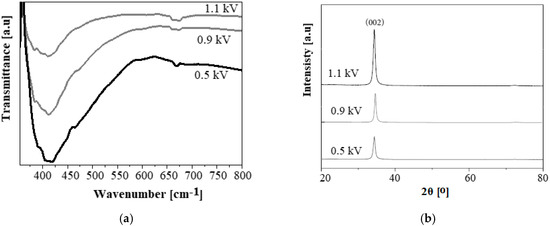
Figure 1.
(a) FTIR spectra of ZGO films sputtered at different sputtering voltages and (b) XRD patterns of ZGO films sputtered at different sputtering voltages.

Table 1.
Description of the position and interpretation of FTIR absorption bands of ZGO films.
In the case of similar basic FTIR spectroscopic features, another criterion for the selection of the most suitable film should be considered. This could be the surface roughness of the coatings, which is expected to be smaller than 10% of the total film thickness for reliable electrical contact [28]. It is known that the sputtering voltage is responsible for the deposition rate and the energy of the particles incoming to the surface of the substrate during the film’s growth [29]. Therefore, the smoothness of the films sputtered at various voltages is expected to differ. At the piezoelectric nanogenerators and other miniaturized energy harvesting systems, the problems with the rough contacting layers result in energy loss. This manifested as a voltage drop or power dissipation over a great contact resistance, which can be formed due to low contact area at the films interfaces.
XRD patterns of the ZGO thin films as a function of the sputtering voltage are shown in Figure 1b. The films exhibited one peak, corresponding to the (002) plane situated at 2θ 34.05°, 34.12°, and 34.19°, respectively, for the films sputtered at 0.5, 0.9, and 1.1 kV. The corresponding values of the full width at half maximum (FWHM) and the lattice constant (c) were 0.627, 0.480, 0.388, and 0.5261, 0.5252, 0.5242, respectively for the films sputtered at 0.5, 0.9, and 1.1 kV. The intensity of the (002) peak increased when the sputtering voltage increased, which suggests that ZGO thin films deposited at higher voltage have a better crystalline structure, because of the greater energy of the sputtered particles, resulting in better lattice arrangement due to the migration of the particles while taking an energetically favorable position. Therefore, the number of thin-film defects decreased, the crystallization of the films was enhanced, and the FWHM decreased. The strain can be calculated considering its relation to the FWHM value, Bragg’s angle, and the wavelength of the X-ray. This relation can be found elsewhere [30]. The minimum value of the strain of 7 × 10⁻³ was obtained at the maximum value of the sputtering voltage (1.1 kV) and increased in a linear manner to 11 × 10−3 as the sputtering voltage decreased to 0.5 kV. The results are in good agreement with a recent report [31].
The SEM images of ZGO films deposited at various sputtering voltages are shown in Figure 2a–c. The surfaces of the films are characterized with high density and continuity, no matter the growth conditions. At 0.5 kV, as shown in Figure 2a, due to the low energy of the sputtered particles having lower mobility on the surface, the film has higher roughness, which was further confirmed by the AFM measurements. At 0.9 kV, as shown in Figure 2b, no significant change could be noted and the surface morphology was very close to that observed at 0.5 kV. More precise analysis by AFM revealed a slight decrease in the roughness. More significant change could be observed at 1.1 kV, where the highly energetic sputtered particles increased the probability of nucleation reaching the substrate. This increase in the number of sites for grain growth, resulted in smaller crystal size and lower surface roughness.
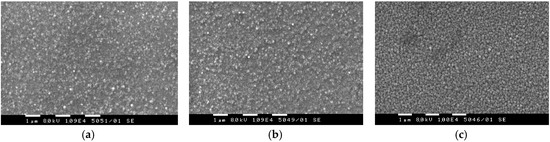
Figure 2.
SEM images of ZGO films sputtered at: (a) 0.5 kV; (b) 0.9 kV; (c) 1.1 kV.
AFM topographies of the ZGO thin films as a function of the sputtering voltage are shown in Figure 3a–c.
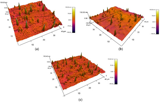
Figure 3.
3D topography of ZGO films with the corresponding root mean square (RMS) roughness and sputtering voltage: (a) RMS roughness 16.77 nm, 0.5 kV; (b) RMS roughness 15.56 nm, 0.9 kV and (c) RMS roughness 12.90 nm, 1.1 kV.
As can be seen, the film sputtered at the lowest voltage, as shown in Figure 3a exhibited the greatest root mean square (RMS) roughness of 16.77 nm, which is 11% of the film thickness, produced at 0.5 kV. Although there was a relatively small number of peaks, as compared to the films sputtered at higher voltage, their magnitude was high and they are sharper. This can be ascribed to the low energy of the sputtered particles, which cannot migrate to decrease the free surface energy when reaching the substrate [32]. For this reason, the sample coated with ZnO:Ga2O3 at the lowest sputtering voltage was considered as a starting point of comparison because it is believed that, near this field strength, the sputtered particles’ energy was rather low to allow for proper arrangement by migration and the heaping-free surface of the film [33]. Figure 3b shows that the increase in the sputtering voltage with 400 V resulted in smaller RMS roughness up to 15.56 nm, which is 10% of the film thickness, produced at 0.9 kV. Although it was observed that the coating has a smooth surface among the peaks, they are still sharp and elevated. Finally, it was shown in Figure 3c that the highest sputtering voltage of 1.1 kV led to the lowest RMS roughness of 12.90 nm, which is 9% of the film thickness. This could be due to the smaller height of the peaks with more uniform distribution. The greatest energy of the sputtered particles in this case results in their migration as, when approaching the substrate, they get an energetically more favorable state, reducing the free surface energy and forming more regular coating. The existing small peaks are due to the higher sputtering rate, as compared to the growth rate for the coatings sputtered at 0.5 kV and 0.9 kV [34]. The measurements were conducted in four different locations on the surface of the film, with an area of 1600 µm2, showing an average deviation of 0.76 nm, indicating negligible location-to-location differences in the roughness. Two locations were chosen near the center of the substrate and two locations along the edges. The analyses for two samples of the same type were used to compare sample-to-sample variations, which were also less than 1 nm. Thus, the results were estimated as sufficiently reliable to be representative for the whole surface and we consider the cited values for the roughness as reliable. Thus, based on the criterion for smaller roughness, the film sputtered at 1.1 kV was selected for further XPS analysis, as shown in Figure 4 and Figure 5, and for the fabrication of the nanogenerator structure and electromechanical testing.
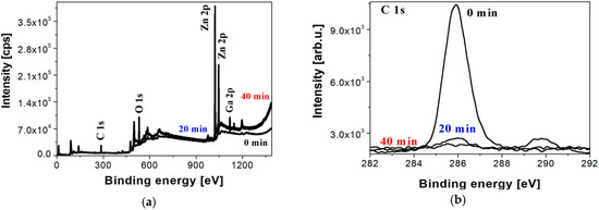
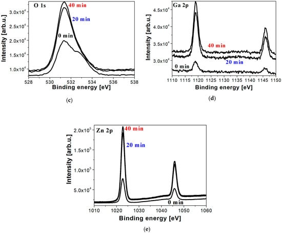
Figure 4.
XPS study of ZGO film sputtered at 1.1 kV, performed on the film before and after Ar+ etching for 20 and 40 min, where (a) presents XPS wide survey spectra and (b–e) show XPS spectra in C1s, O1s, Ga2p and Zn 2p regions of ZGO film, respectively.
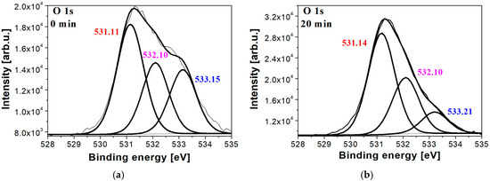
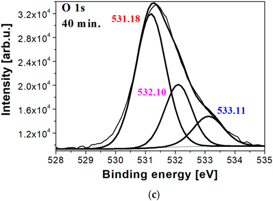
Figure 5.
Deconvolution of the O 1s XPS spectrum of the ZGO film sputtered at 1.1 kV (a) before and (b,c) after Ar+ etching for 20 and 40 min, respectively
The wide-scan XPS spectra (binding energy from 0 to 1300 eV) of the films, deposited at sputtering voltages 0.5 and 1.1 kV, were taken, but only those of the films deposited at 1.1 kV were shown because of their optimal piezoelectric performance, as shown in Figure 4a. There are lines at 89 eV (due to Zn p3/2 in ZnO), 106.7 eV (Ga 3p 3/2–Ga2O3), 139.9 eV (Zn 3s, ZnO), 161.01 (Ga 3s, Ga2O3), and 1197 (Zn 2s, ZnO). These lines also confirm the presence of Zn and Ga in the oxidation state. There are some unidentified peaks, but with small intensities. The XPS survey spectra confirmed the existence of Ga, Zn, and O in the samples, as well as the presence of carbon contaminants, which can be monitored in the C 1s region, as shown in Figure 4b–e. The carbon component in the sputtered films can be attributed to contamination, which resulted from the samples being exposed to the ambient atmosphere and/or the oil diffusion pump in the sputtering process [35]. XPS analysis reveals that there is carbon contamination, which can be monitored in the C 1s region. The depth profile shows that, on the film surfaces, carbon concentration was very high (around 55 at.%) but it drops drastically after 20 and 40 min Ar+ etching up to 1.5–3.4 at.%. The deconvolution of C 1s spectra consists of four peaks. The typical chemical components associated with adventitious carbon were observed, which were attributed to C–C (284.8 eV), C–O (286.0 eV), and CO3 (288.4 eV) [36]. The peaks at 285.30 eV can be also related to the bonding between carbon atoms, which was possibly caused by the carbon precipitates or clusters in this film and components at 289 eV, due to carbon contamination (C=C) [37]. After Ar sputtering for 20 and 40 min, the carbon peak intensity was reduced, but it still exists and a small amount of carbon can be observed in the film structure.
The Zn 2p spectra contained a doublet, and the two peaks are identified as Zn 2p3/2 and Zn 2p 1/2 with a difference of 23.1 eV in the binding energy between these two peaks. These values are consistent with those reported in [38]. The Zn 2p3/2 photoelectron peaks are above 1022.77 eV and the binding energy values are higher than the binding energy of the metal Zn (1021.1 eV), which indicates that Zn was in a +2 oxidation state [39]. The XPS spectra of the Zn 2p core levels exhibit symmetric shapes, which was a sign that no multi valence states of Zn were present and the Zn 2p3/2 and Zn 2p 1/2 peaks can confirm the wurtzite structure, favorable for piezoelectric applications [40].
The characteristic binding energy values of 1118.96–1119.18 and 1145.75–1146.07 eV for Ga 2p3/2 and Ga 2p1/2, as well as their symmetry shapes, revealed that the gallium exists only in a trivalent oxidation state. The obtained results show that Ga2+ was successfully incorporated in the ZnO lattice by substituting the Zn sites [41]. The XPS spectra of Zn 2p and Ga 2p show no obvious differences upon Ar ion etching in respect to the values of the binding energies and the intensities of the Zn 2p and Ga 2p peaks were changed as, on the film surfaces their intensities were lower and increased after 20 and 40 min etching, as shown in Figure 4d,e. The presence of Ga–O bonds has been deduced from the FTIR spectra of sputtered ZGO films, as shown in the FTIR results.
The deconvolution of the O 1 s XPS spectrum before and after Ar+ the etching of the ZGO film sputtered at 1.1 kV is shown in Figure 5a–c. The asymmetry of the O 1s photoelectron peak was related to the existence of different forms of oxygen bonds. The O 1s spectra can be resolved into three nearly Gaussian distribution peaks approximately centered at 531.11, 532.10, and 533.15 eV. It must be noted that the highest asymmetry was manifested for the O 1s spectra measured on the film surfaces and, after Ar etching, the oxygen peak intensity increases. The low binding energy line around 531 eV was attributed to O 1s mainly corresponding to the O2– in wurtzite ZnO [42]. The peak at 532.10 eV can be associated with absorbed species, such as C–O bond, a hydroxyl group, or even adsorbed O2 [43]. The hydroxyl groups and water inclusion can be ignored as a previous FTIR study clearly exhibits that there are no characteristic absorption features related to hydroxyl group stretching and bending vibrations. C–O bonds were detected by FTIR analysis, but this could be due to the atmospheric ambient. The highest energy component of the O 1s peak near 533.15 eV can be assigned to the oxygen vacancies within the ZnO matrix or to interstitial oxygen (Oi) [44]. Despite the sputtering time, the peak located at 531.11 eV dominates the composition of the O1s peak, indicating that this oxygen signal mainly comes from the Zn–O bond. XPS measurements were performed as well as measurements for the ZnO:Ga2O3 films deposited at the sputtering voltage 0.5 kV. The obtained results are very close and the tendency of the evolution of O1s, Zn 2p, and Ga2p spectra with etching are similar, while no new features were found between the films obtained at different sputtering voltages. A closer study of the Zn2p and Ga2p spectra shows that their shapes are symmetrical, revealing that Zn exists in only a +2 oxidation state and the gallium only in a trivalent oxidation state. The third component of the O1 s spectrum at the binding energy of 533 eV for the film, deposited at lower sputtering voltage, reveals slightly higher integrated areas of this peak, indicating the higher concentration of oxygen vacancies or interstitial oxygen.
Joshi et al. have reported results on the influence of the oxygen vacancies on the polarization processes in oxides containing piezoelectric ceramic films; however, a noticeable influence was observed at an oxygen concentration difference of at least 4% [45]. Moreover, it has been found that the oxygen deficiency results in a reduction in domain wall mobility and domain switching difficulties, which is more important for applications, requiring fast detection response, such as sensors, and those requiring low voltage for motion activation, such as actuators, rather than for harvesting applications.
Quantitative analysis of the elemental composition of the ZGO films, deposited at the two sputtering voltages, was performed and the results for 0, 20, and 40 min of Ar+ etching arre summarized in Table 2 and Table 3 The distribution of the atomic concentration of elements from the surface to the depth of the studied film show that at the surface absorption of contaminations takes place, which can explain the great percentage of carbon, which, however, decreased with the layer-by-layer removal. Regarding the presence of the Ga and Zn in the total composition, it matches the composition ratio of the sputtering target, according to the certificate for the analysis of the substance [46]. This is proof for suitable growth mode, which did not change the stoichiometry of the film. The distribution of the useful components was quite similar after 20 min and 40 min of etching, which was evidence for a uniform chemical composition across the sample.
Table 2.
Atomic percentage concentration of the elements in ZGO film, deposited at the sputtering voltage 1.1 kV after 0, 20, and 40 min of etching.
Table 3.
Atomic percentage concentration of the elements in ZGO film, deposited at the sputtering voltage 0.5 kV after 0, 20, and 40 min of etching.
The conclusions from the XPS study are that the sputtered ZnO:Ga films are oxygen-rich, Ga was successfully incorporated in ZnO matrix, the Zn 2p peaks correspond to the wurtzite ZnO, and there is a small amount of carbon contamination within the film structure. The oxygen concentration difference in the films sputtered at 0.5 and 1.1 kV, even after argon etching of 40 nm, was less than 3%, assuming the lower contribution of the oxygen vacancy to the device performance.
The results from the piezoelectric response of the samples produced at the three sputtering voltages indicated that the film, deposited at the highest sputtering voltage, possesses optimal performance, and this can be attributed to the reduction in the surface roughness. To demonstrate the energy harvesting behavior of the ZGO films produced at a sputtering voltage of 1.1 kV, a simple flexible energy harvesting element was fabricated and the electrical characteristics were measured. The electromechanical testing was performed in cantilever beam mode with a laboratory-made vibrational setup. The oscillogram presented in Figure 6 is related to vibration with a frequency of 50 Hz and applied a mass loading equivalent to 100 g/cm2.
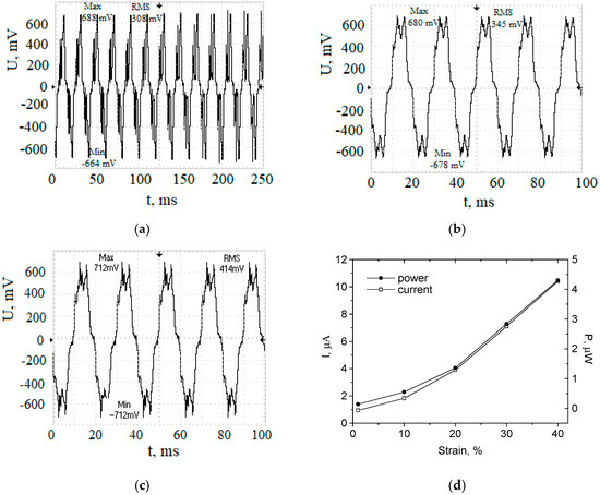
Figure 6.
Piezoelectric voltage produced at a relatively low mass load of 100 g/50Hz from Ag/ZnO:Ga2O3/Ag harvester, incorporating piezoelectric film sputtered at: (a) 0.5 kV; (b) 0.9 kV; (c) 1.1. kV; (d) current and power generated vs. strain for the structure with the optimal piezoelectric film sputtered at 1.1 kV.
To characterize the intrinsic conversion ability of the piezoelectric generators, the power output is often measured through the product of the open-circuit voltage and short-circuit current [47]. The open-circuit voltage is requested for precise peak detection at the input of the power management integrated circuits [48]. It should be noted that the RMS value of the AC electrical signals is significant for the output energy estimation. Figure 6a shows the piezoelectric voltage of the device, using film produced at 0.5 kV. It was characterized with lack of symmetry in the amplitude values of the positive and negative semi-waves (Umax = 688 mV; Umin = −664 mV). The lowest RMS voltage of 308 mV was detected. The results can be ascribed to the lowest degree of crystallinity, lowest piezoelectric film density, and the highest surface roughness. Increasing the sputtering voltage during ZGO film growth resulted in the enhancement of their microstructural and morphological features, as was previously discussed. This improved the piezoelectric performance, provided better symmetry of the voltage with comparable amplitude (Umax = 680 mV; Umin = −678 mV), and increased the RMS value to 345 mV, as shown in Figure 6b. The best electrical performance was observed for the device produced at sputtering voltage 1.1 kV. In this case, The Ag/ZnO:Ga2O3/Ag harvester produced periodical signal with excellent symmetry, as shown in Figure 6c (Umax = 712 mV; Umin = −712 mV). In addition to the symmetry in the magnitude of the pulses, their width was more regular. The highest voltage magnitude and the highest RMS 414 mV were measured (70 mV higher than the structure with film sputtered at 0.9 kV and ~100 mV higher than the case of 0.5 kV). The non-linear distortions can be ascribed to the point contacting with the peaks of the coating, detected by AFM. The current was in the microampere range, with good, near to linear dependence on the strain, making the power output practically useful, as shown in Figure 6d. For comparison, the current measured from the devices at the sputtering voltage of the ZGO films, 0.5 and 0.9 kV, were in the nanoampere range even at the maximum strain—approximately 900 and 980 nA, respectively.
Considering the relation between the stress, strain, and Young’s modulus [49] and taking into account that the area of 3 cm2 of the sample experiencing the force load, as well as assuming Young modulus of 130 GPa of sputtered Ga-doped ZnO films [50], it was found that the strain varied in the range 1–40%. The current of 10.4 µA was the maximal current produced as a result of strain equal to 40%. The value was in the microamperes range, as compared to the typical values reported for ZnO films, having similar thickness, due to gallium doping. Figure 6d shows the short circuit current and the output power plotted versus the strain for the Ag/ZnO:Ga2O3/Ag structure, counting the current measurement error of ±300 nA, typical for the set measurement range. The results of the output electric power of 0.14–4.3 µW for this strain range are in good agreement with those recently reported [51] and these values are typical for the piezoelectric thin film nanogenerators.
Compared with some of the most popular publications in the field, using lead-free materials with a similar design (sandwich type) revealed that the proposed ZGO energy harvesting element exhibited great potential for vibrational energy conversion by using thinner films, smaller sizes of the harvesting element and conventional (non-chemical) microfabrication technology in comparison with those reported in the literature, as shown in Table 4. The power density was comparable and, in some cases, even exceeding that reported, considering the difference in the functional film area and the operational frequency remaining in the low-frequency range.
Table 4.
Comparison of the energy harvesting performance of elements with a similar design, involving lead-free materials.
4. Conclusions
Thin films of ZnO, doped by Ga2O3 are deposited by RF sputtering. The variation in the deposition conditions resulted in tuning their morphology by keeping their bond types and chemical states. AFM study of the ZGO reveals that the films sputtered at the highest voltage of 1.1 kV exhibited the lowest surface roughness. The typical absorption bands for the piezoelectric phase are confirmed by FTIR and XPS spectroscopies. The surfaces of the films were characterized with high density and continuity. A simple single-layer energy harvesting element was designed and fabricated. High piezoelectric current and power were measured in comparison with the device implementing ZnO, making the films suitable for the abovementioned application. It was found that the device performance was more sensitive to the piezoelectric films’ surface roughness rather than to the presence of oxygen vacancies, whose concentration was limited in all cases of sputtering conditions. Future work will be related to studying the effect of the film thickness of ZGO for the films produced at the optimal sputtering voltage on the piezoelectric energy harvesting performance.
Author Contributions
Conceptualization, M.A.; methodology, M.A. and K.G.; validation, T.I. and F.H.; formal analysis, M.A., T.I., and F.H.; investigation, M.A, V.S., and F.H.; data curation, M.A, V.S., T.I., and F.H.; writing—original draft preparation, M.A.; writing—review and editing, K.G. and T.I.; visualization, M.A.; supervision, K.G.; project administration, M.A.; funding acquisition, M.A. All authors have read and agreed to the published version of the manuscript.
Funding
This research was funded by the Bulgarian National Science Fund, grant number DH 07/13.
Acknowledgments
The authors acknowledge Armin Gölzhäuser for the provided XPS facility and Sascha Koch for the XPS measurements.
Conflicts of Interest
The authors declare no conflict of interest.
References
- Wei, H.; Wang, H.; Xia, Y.; Cui, D.; Shi, Y.; Dong, M.; Liu, C.; Ding, T.; Zhang, J.; Ma, Y.; et al. An overview of lead-free piezoelectric materials and devices. J. Mater. Chem. C 2018, 6, 12446–12467. [Google Scholar] [CrossRef]
- Liu, Q.; Zhang, Y.; Gao, J.; Zhou, Z.; Wang, H.; Wang, K.; Zhang, X.; Lia, L.; Li, J.-F. High-performance lead-free piezoelectrics with local structural heterogeneity. Energy Environ. Sci. 2018, 11, 3531–3539. [Google Scholar] [CrossRef]
- Wu, J. Advances in Lead-Free Piezoelectric Materials; Springer Nature: Singapore, 2018. [Google Scholar]
- Wang, P.; Du, H. ZnO thin film piezoelectric MEMS vibration energy harvesters with two piezoelectric elements for higher output performance. Rev. Sci. Instrum. 2015, 86, 075002. [Google Scholar] [CrossRef] [PubMed]
- Rahman, W.; Garain, S.; Sultana, A.; Middya, T.R.; Mandal, D. Self-powered piezoelectric nanogenerator based on wurtzite zno nanoparticles for energy harvesting application. Mater. Today Proc. 2018, 5, 9826–9830. [Google Scholar] [CrossRef]
- Morisot, F.; Nguyen, V.H.; Montemont, C.; Maindron, T.; Muñoz-Rojas, D.; Mouis, M.; Langlet, M.; Ternon, C. Al2O3, Al doped ZnO and SnO2 encapsulation of randomly oriented ZnO nanowire networks for high performance and stable electrical devices. Nanotechnology 2019, 30, 385202. [Google Scholar] [CrossRef]
- Zhao, H.; Hu, J.; Chen, S.; Xie, Q.; He, J. High nonlinearity and high voltage gradient ZnO varistor ceramics tailored by combining Ga2O3, Al2O3, and Y2O3 dopants. J. Am. Ceram. Soc. 2016, 99, 769–772. [Google Scholar] [CrossRef]
- Parida, B.; Jeong, S.; Kim, H. Effects of Al diffusion process on the electrical, optical, and structural properties of transparent conducting Al-doped ZnO. J. Korean Phys. Soc. 2018, 73, 917–921. [Google Scholar] [CrossRef]
- Gu, J.H.; Lu, Z.; Long, L.; Zhong, Z.Y.; Yang, C.Y.; Hou, J. Preparation, structure and optical properties of transparent conducting gallium-doped zinc oxide thin films. Mater. Sci. Pol. 2015, 33, 470–481. [Google Scholar] [CrossRef]
- Zhao, H.; Hu, J.; Chen, S.; Xie, Q.; He, J. Tailoring the high-impulse current discharge capability of ZnO varistor ceramics by doping with Ga2O3. Ceram. Int. 2016, 42, 5582–5586. [Google Scholar] [CrossRef]
- Hyman, D.; Mehregany, M. Contact physics of gold microcontacts for MEMS switches. IEEE Trans. Compon. Pack. T. 1999, 22, 357–364. [Google Scholar] [CrossRef]
- Pennec, F.; Peyrou, D.; Leray, D.; Pons, P.; Plana, R.; Courtade, F. Impact of the surface roughness description on the electrical contact resistance of ohmic switches under low actuation forces. IEEE Trans. Compon. Pack. T. 2012, 2, 85–94. [Google Scholar] [CrossRef]
- Fu, X.; Gao, L.; Zhang, Q.; Liu, Q. Surface roughness research of piezoelectric self-adaptive micro-EDM. Procedia CIRP 2016, 42, 563–568. [Google Scholar] [CrossRef]
- Aleksandrova, M. Polymeric seed layer as a simple approach for nanostructuring of Ga-doped ZnO films for flexible piezoelectric energy harvesting. Microelectron. Eng. (In Press).
- Skinner, S. Energy Storage and Conversion Materials; Royal Society of Chemistry: Croydon, UK, 2019. [Google Scholar]
- Zhao, H.; He, J.; Hu, J.; Chen, S.; Xie, Q. High nonlinearity and low residual-voltage ZnO varistor ceramics by synchronously doping Ga2O3 and Al2O3. Mater. Lett. 2016, 164, 80–83. [Google Scholar] [CrossRef]
- Reinhardt, K.; Kern, W. Handbook of Silicon Wafer Cleaning Technology; William Andrew: Oxford, UK, 2018. [Google Scholar]
- Aleksandrova, M.; Kolev, G.; Vucheva, Y.; Pathan, H.; Denishev, K. Characterization of piezoelectric microgenerator with nanobranched zno grown on a polymer coated flexible substrate. Appl. Sci. 2017, 7, 890. [Google Scholar] [CrossRef]
- Kwon, Y.J.; Kim, K.H.; Lim, C.S.; Shim, K.B. Characterization of ZnO nanopowders synthesized by the polymerized complex method via an organochemical route. J. Ceram. Process. Res. 2002, 3, 146–149. [Google Scholar]
- Khan, Z.R.; Khan, M.S.; Zulfequar, M.; Khan, M.S. Optical and structural properties of ZnO thin films fabricated by sol-gel method. Mater. Sci. Appl. 2011, 2, 340–345. [Google Scholar] [CrossRef]
- Goswami, N.; Sahai, A. Structural transformation in nickel doped zinc oxide nanostructures. Mater. Res. Bull. 2013, 48, 346–351. [Google Scholar] [CrossRef]
- Ghazali, N.M.; Mahmood, M.R.; Yasui, K.; Hashim, A.M. Electrochemically deposited gallium oxide nanostructures on silicon substrates. Nanoscale Res. Lett. 2014, 9, 120. [Google Scholar] [CrossRef]
- Music, S.; Dragovic, D.; Popovic, S. Influence of synthesis route on the formation of ZnO particles and their morphologies. J. Alloy. Compd. 2007, 429, 242–249. [Google Scholar] [CrossRef]
- Yang, J.; Zhao, Y.; Frost, R.L. Infrared and infrared emission spectroscopy of gallium oxide α-GaO(OH) nanostructures. Spectrochem. Acta A Mol. Biomol. Spetroscopy 2009, 74, 398–403. [Google Scholar] [CrossRef] [PubMed]
- Ravichandrana, K.; Rathi, R.; Baneto, M.; Karthika, K.; Rajkumar, P.V.; Sakthivel, B.; Damodaran, R. Effect of Fe+F doping on the antibacterial activity of ZnO powder. Ceram. Int. 2015, 41, 3390–3395. [Google Scholar] [CrossRef]
- Zunke, I.; Heft, A.; Schäfer, P.; Haidu, F.; Lehmann, D.; Grünler, B.; Schimanski, A.; Zahn, D.R.T. Conductive zinc oxide thin film coatings by combustion chemical vapour deposition at atmospheric pressure. Thin Solid Film. 2013, 532, 50–55. [Google Scholar] [CrossRef]
- Petrović, Ž.; Ristić, M.; Musić, S. Development of ZnO microstructures produced by rapid hydrolysis of zinc acetylacetonate. Ceram. Int. 2014, 40, 10953–10959. [Google Scholar] [CrossRef]
- Khan, A.; Abas, Z.; Kim, H.S.; Oh, I.K. Piezoelectric thin films: An integrated review of transducers and energy harvesting. Smart Mater. Struct. 2016, 25, 053002. [Google Scholar] [CrossRef]
- Hamaguchi, S. Plasma-surface Interactions in Material Processing. J. Phys. Conf. Ser. 2010, 257, 012007. [Google Scholar] [CrossRef]
- Liu, W.; Du, G.; Sun, Y.; Xu, Y.; Yang, T.; Wang, X.; Chang, Y.; Qiu, F. Al-doped ZnO thin films deposited by reactive frequency magnetron sputtering: H2-induced property changes. Thin Solid Film. 2007, 515, 3057–3060. [Google Scholar] [CrossRef]
- Chen, Y.; Hu, Y.; Meng, Q.; Yan, H.; Shuai, W.; Zhang, Z. Natively textured surface of Ga-doped ZnO films electron transporting layer for perovskite solar cells: Further performance analysis from device simulation. J. Mater. Sci. Mater. Electron. 2019, 30, 4726–4736. [Google Scholar] [CrossRef]
- Greene, J.E. Tracing the recorded history of thin-film sputter deposition: From the 1800s to 2017 featured. J. Vac. Sci. Technol. A 2017, 35, 05C204. [Google Scholar] [CrossRef]
- Frey, H.; Khan, H.R. Handbook of Thin Film Technology; Springer Science & Business Media: Berlin, Germany, 2015. [Google Scholar]
- Hashimi, S. Comprehensive Materials Processing; Elsevier: Amsterdam, The Netherlands, 2014. [Google Scholar]
- You, Z.Z.; Hua, G.J. Electrical, optical and microstructural properties of transparent conducting GZO thin films deposited by magnetron sputtering. J. Alloy. Comp. 2012, 530, 11–17. [Google Scholar] [CrossRef]
- Alfaro Cruz, M.R.; Ceballos-Sanchez, O.; Luévano-Hipólito, E.; Torres-Martínez, L.M. ZnO thin films deposited by RF magnetron sputtering: Effects of the annealing and atmosphere conditions on the photocatalytic hydrogen production. Intern. J. Hydrog. Energy 2018, 43, 10301–10310. [Google Scholar] [CrossRef]
- Kim, D.; Hwang, I.; Son, J.; Kim, H. Inductively coupled-plasma dry etching of a ZnO thin film by Ar-diluted CF4 gas. J. Korean Phys. Soc. 2011, 58, 1536–1540. [Google Scholar] [CrossRef]
- Li, G.; Wang, H.; Wang, Q.; Zhao, Y.; Wang, Z.; Du, J.; Ma, Y. Structure and properties of Co-doped ZnO films prepared by thermal oxidization under a high magnetic field. Nanoscale Res. Lett. 2015, 10, 112. [Google Scholar] [CrossRef]
- Khokhra, R.; Bharti, B.; Lee, H.N.; Kumar, R. Visible and UV photo-detection in ZnO nanostructured thin films via simple tuning of solution method. Sci. Rep. 2017, 7, 15032. [Google Scholar] [CrossRef] [PubMed]
- Hosseini, S.M.; Abdolhosseini, I.; Kameli, S.P.; Salamati, H. Effect of Ag doping on structural, optical, and photocatalytic properties of ZnO nanoparticles. J. Alloy. Compd. 2015, 640, 408–415. [Google Scholar] [CrossRef]
- Kim, S.; Seo, J.; Jang, H.W.; Bang, J.; Lee, W.; Lee, T.; Myoung, J.-M. Effects of H 2 ambient annealing in fully 0 0 2-textured ZnO:Ga thin films grown on glass substrates using RF magnetron co-sputter deposition. Appl. Surf. Sci. 2009, 255, 4616–4622. [Google Scholar] [CrossRef]
- Caglar, Y.; Caglar, M.; Ilican, S. XRD, SEM, XPS studies of Sb doped ZnO films and electrical properties of its based Schottky diodes. Optik 2018, 164, 424–432. [Google Scholar] [CrossRef]
- Abdel-Wahab, M.S.; Jilani, A.; Yahia, I.S.; Al-Ghamdi, A.A. Enhanced the photocatalytic activity of Ni-doped ZnO thin films: Morphological, optical and XPS analysis. Superlattice. Microstruct. 2016, 94, 108–118. [Google Scholar] [CrossRef]
- Saaedi, A.; Yousefi, R.; Jamali-Sheini, F.; Zak, A.K.; Cheraghizade, M.; Mahmoudian, M.R.; Baghchaesara, M.A.; Dezaki, A.S. XPS studies and photocurrent applications of alkali-metals-doped ZnO nanoparticles under visible illumination conditions. Physica E 2016, 79, 113–118. [Google Scholar] [CrossRef]
- Joshi, A.; Rauch, J.-Y.; Bodas, D.; Gangal, S. Effect of oxygen vacancies on crystallization and piezoelectric performance of PZT. Ferroelectrics. 2016, 494, 117–122. [Google Scholar]
- Kurt Lesker Company. Zinc Gallium Oxide (Pieces). Available online: https://www.lesker.com/msds/pdfs/2e3d1f05d1b63e7e6db640f6b90980b76759deebf309560e5d6f9fd483e0cd54.pdf (accessed on 30 May 2020).
- Briscoe, J.; Jalali, N.; Woolliams, P.; Stewart, M.; Weaver, P.M.; Cain, M.; Dunn, S. Measurement techniques for piezoelectric nanogenerators. Energy Environ. Sci. 2013, 6, 3035–3045. [Google Scholar] [CrossRef]
- Chen, K.-H. Power Management Techniques for Integrated Circuit Design; John Wiley & Sons: Singapore, 2016. [Google Scholar]
- Collins, D. Mechanical Properties of Materials: Stress and Strain. Available online: https://www.linearmotiontips.com/mechanical-properties-of-materials-stress-and-strain/ (accessed on 5 July 2020).
- Yamamoto, N.; Makino, H.; Yamamoto, T. Young’s modulus and coefficient of linear thermal expansion of ZnO conductive and transparent ultra-thin films. Adv. Mat. Sci. Eng. 2011, 2011, 136127. [Google Scholar] [CrossRef][Green Version]
- Choi, H.Y.; Jeong, Y.G. Microstructures and piezoelectric performance of eco-friendly composite films based on nanocellulose and barium titanate nanoparticle. Compos. Part B Eng. 2019, 168, 58–65. [Google Scholar] [CrossRef]
- Marzencki, M.; Basrour, S.; Charlot, B.M.; Grasso, A.; Colin, M.; Valbin, L. Design and fabrication of piezoelectric micro power generators for autonomous microsystems. In Proceedings of the Design, Test, Integration and Packaging of MEMS/MOEMS, Montreux, Switzerland, 1–3 June 2005; pp. 299–302. [Google Scholar]
- Stassi, S.; Cauda, V.; Ottone, C.; Chiodoni, A.; Pirri, C.F.; Canavese, G. Flexible piezoelectric energy nanogenerator based on ZnO nanotubes hosted in a polycarbonate membrane. Nano Energy 2015, 13, 474–481. [Google Scholar] [CrossRef]
- Fakhri, P.; Amini, B.; Bagherzadeh, R.; Kashfi, M.; Latifi, M.; Yavari, N.; Kanice, S.A.; Kong, L. Flexible hybrid structure piezoelectric nanogenerator based on ZnO nanorod/PVDF nanofibers with improved output. RSC Adv. 2019, 9, 10117–10123. [Google Scholar] [CrossRef]
- Aleksandrova, M.; Ivanova, T.; Koch, S.; Hamelmann, F.; Karashanova, D.; Gesheva, K. Study of sputtered barium strontium titanate films for energy harvesting applications. Adv. Mater. Lett. in press.


© 2020 by the authors. Licensee MDPI, Basel, Switzerland. This article is an open access article distributed under the terms and conditions of the Creative Commons Attribution (CC BY) license (http://creativecommons.org/licenses/by/4.0/).