Article

Effect of Oxygen Source on the Various Properties of SnO2 Thin Films Deposited by Plasma-Enhanced Atomic Layer Deposition

1
Department of Materials Science and Engineering, Seoul National University of Science and Technology, Seoul 01811, Korea
2
Division of Advanced Materials, Korea Research Institute of Chemical Technology (KRICT), 141 Gajeong-Ro, Yuseong-Gu, Daejeon 34114, Korea
*
Author to whom correspondence should be addressed.
Coatings 2020, 10(7), 692; https://doi.org/10.3390/coatings10070692
Submission received: 13 June 2020 / Revised: 11 July 2020 / Accepted: 14 July 2020 / Published: 18 July 2020
(This article belongs to the Special Issue Thin Films by Atomic Layer Deposition: Properties and Applications)

Abstract

:
Herein, we performed a comparative study of plasma-enhanced atomic layer deposition (PEALD) of SnO2 films using Sn(dmamp)2 as the Sn source and either H2O plasma or O2 plasma as the oxygen source in a wide temperature range of 100–300 °C. Since the type of oxygen source employed in PEALD determines the growth behavior and resultant film properties, we investigated the growth feature of both SnO2 PEALD processes and the various chemical, structural, morphological, optical, and electrical properties of SnO2 films, depending on the oxygen source. SnO2 films from Sn(dmamp)2/H2O plasma (SH-SnO2) and Sn(dmamp)2/O2 plasma (SO-SnO2) showed self-limiting atomic layer deposition (ALD) growth behavior with growth rates of ~0.21 and 0.07–0.13 nm/cycle, respectively. SO-SnO2 films showed relatively larger grain structures than SH-SnO2 films at all temperatures. Interestingly, SH-SnO2 films grown at high temperatures of 250 and 300 °C presented porous rod-shaped surface morphology. SO-SnO2 films showed good electrical properties, such as high mobility up to 27 cm2 V−1·s−1 and high carrier concentration of ~1019 cm−3, whereas SH-SnO2 films exhibited poor Hall mobility of 0.3–1.4 cm2 V−1·s−1 and moderate carrier concentration of 1 × 10¹⁷–30 × 1017 cm−3. This may be attributed to the significant grain boundary and hydrogen impurity scattering.

1. Introduction

Tin(IV) oxide (SnO2) has received considerable research attention due to its excellent electrical conductivity, optical transparency, and chemical stability. This has been extensively utilized in various applications, such as gas sensors, batteries, fuel cells, photovoltaic cells, photodetectors, transparent electronics, and thin film transistors (TFT) [1,2,3,4,5,6,7]. For the growth of high-quality SnO2 thin films, a variety of methods, such as sputtering [8], chemical vapor deposition [9], spray pyrolysis [10], pulsed laser deposition [11], and atomic layer deposition (ALD) [12], have been employed. In particular, the exploitation of ALD SnO2 films for state-of-the-art devices is increasing because ALD can produce dense, uniform, and conformal films on complex three-dimensional substrates at relatively low deposition temperatures [13]. To obtain high-quality ALD SnO2 film at wide process temperatures, various Sn precursors, including Sn halides and metal–organic Sn-precursors in combination with different co-reactants, like H2O, O3, H2O2, and other plasma oxygen sources, have been investigated. Especially, plasma-enhanced atomic layer deposition (PEALD) of SnO2, in which highly reactive radicals are employed as co-reactants, has distinct advantages over thermal SnO2 ALD, e.g., higher growth rates, better film quality, lower impurity concentration, and wider and lower deposition temperature window enabling to grow SnO2 on low-temperature compatible substrates, like polyethylene naphthalate (PEN), polyethylene terephthalate (PET), and other organic containing materials [14]. Moreover, PEALD, using a highly reactive plasma, extends the choice of precursors by allowing the use of less-reactive precursors, which facilitates the growth of thin films that are difficult to deposit with thermal ALD. Wang et al. reported the low-temperature (~100 °C) SnO2 PEALD process using tetrakis(dimethylamino)tin (TDMASn) and O2 plasma at a high growth rate of 0.17 nm/cycle, and a highly efficient perovskite solar cell was demonstrated using 100 °C-deposited SnO2 as an electron-selective layer [15]. Lee et al. explored SnO2 PEALD using halogenated SnCl4 precursor and O2 plasma. This showed improved growth rate, film purity, and crystallinity compared with the thermal ALD process using SnCl4/H2O [16]. However, there is still a lack of precursor combinations for the growth of ALD SnO2 film at broad temperature window.
Therefore, in this study, we investigated the growth behaviors and film characteristics of PEALD SnO2 thin films obtained from dimethylamino-2-methyl-2-propoxy-tin(II) (Sn(dmamp)2) as a Sn precursor and either H2O plasma or O2 plasma as the oxygen source. The chemical, optical, structural, and electrical properties of PEALD SnO2 films, as well as growth features, like self-limiting reaction and growth rate, were characterized depending on the oxygen source over a wide growth temperature range between 100 and 300 °C. In particular, the use of H2O plasma for PEALD SnO2 growth has not been reported yet, and PEALD SnO2 films showed excellent properties of high deposition rate, excellent crystallinity, and low impurity concentration.

2. Experiment

PEALD of SnO2 films was carried out over a wide temperature range from 100 to 300 °C. SnO2 films were deposited by using different Sn precursor/reactant combinations of Sn(dmamp)2/H2O plasma (SH-SnO2) and Sn(dmamp)2/O2 plasma (SO-SnO2) separately. The Sn precursor was transported into the chamber by using N2 (99.9999%) carrier gas of 100 sccm from a bubbler-type canister heated at 60 °C. The gas line for the Sn precursor was maintained at 90 °C to prevent precursor condensation. Deionized H2O was supplied to create H2O plasma from a vapor-type canister at 25 °C. O2 gas (99.999%, 100 sccm) was introduced to produce the O2 plasma reactant. For all experiments, Si and soda-lime glass were used as substrates. All the SnO2 PEALD processes were performed over typical four sequential steps: Sn precursor pulse, N2 purge (10 s, 500 sccm), plasma reactant pulse, and N2 purge (10 s, 500 sccm). The optimized source and reactant pulse lengths were determined separately for each PEALD process.
The thickness and refractive index of the PEALD SnO2 films were determined by ex situ ellipsometry system (FS-1, Film sense, Lincoln, Dearborn, MI, USA) at a wavelength of 635 nm. X-ray photoelectron spectroscopy (XPS, K-Alpha, Thermo Scientific, Waltham, MA, USA) surface analysis was performed to indicate the chemical binding states of the elements and to examine the C and N impurity concentrations. Dynamic secondary ion mass spectrometry (D-SIMS, IMS-4FE7, CAMECA, Gennevilliers, France) was performed to examine the H impurity concentration in the SnO2 films via depth profiling. Ultraviolet–visible spectroscopy (UV–Vis, sepcord200, analytikjena, Jena, Germany) was performed to estimate transmittance and optical band gap of the SnO2 films. Surface morphologies of the SH-SnO2 and SO-SnO2 films grown at various temperatures were observed using high-resolution field-emission scanning electron microscopy (HR-FESEM, SU8010, Hitach, Tokyo, Japan). Film crystallinity of the SnO2 thin films was investigated using glancing-angle X-ray diffraction (GAXRD, D-MAX 2500, Rigaku, Tokyo, Japan). Finally, electrical properties, like carrier concentration, mobility, and resistivity of the SnO2 films on soda-lime glass, were measured by Hall-effect measurements (HMS-3000, ecopia, Anyang, South Korea).

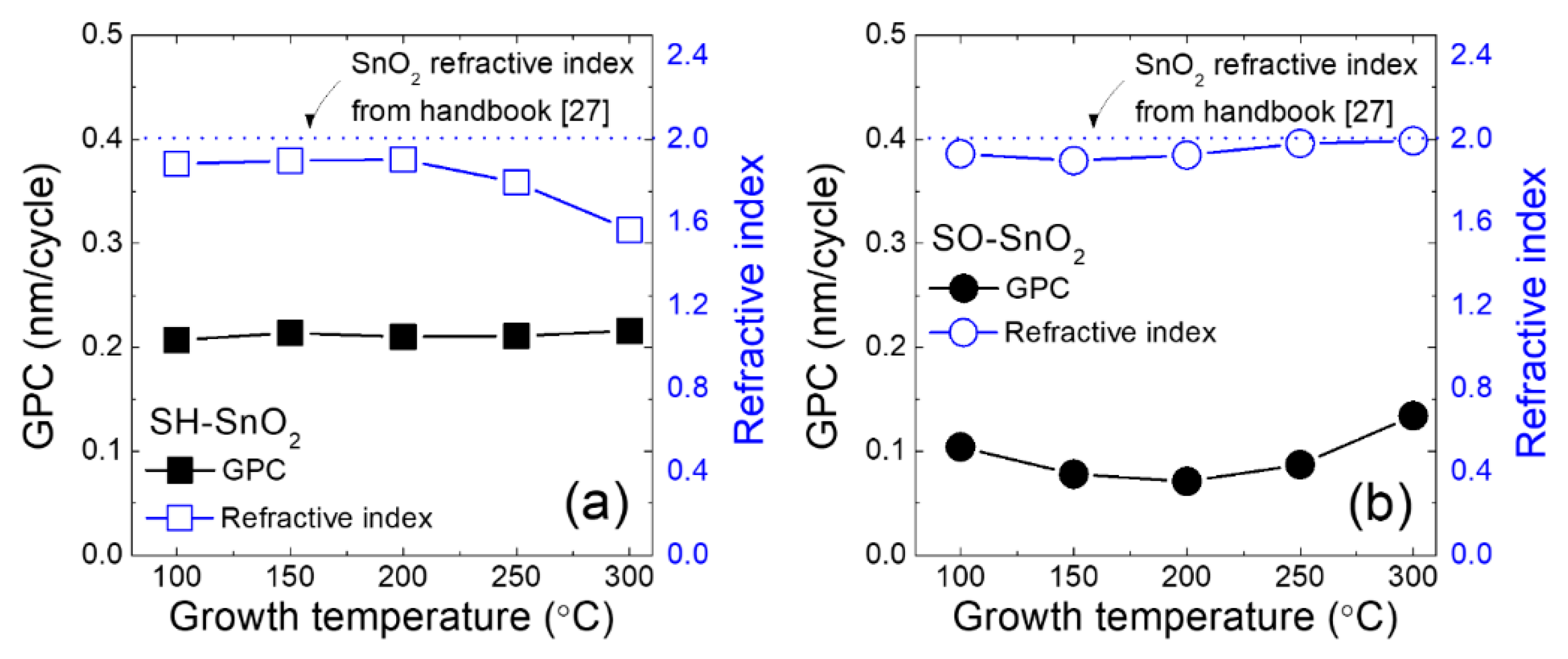
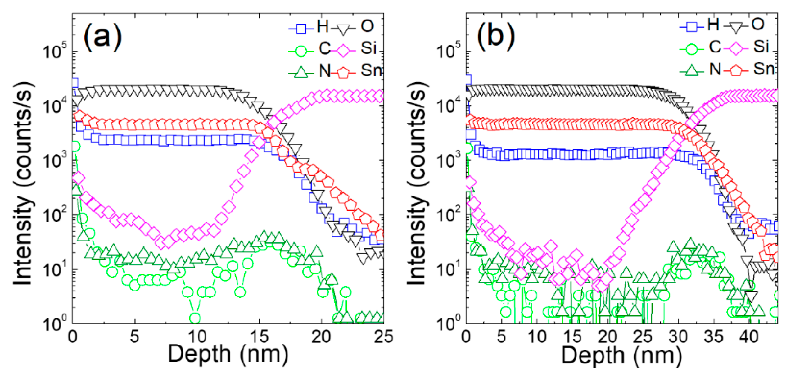
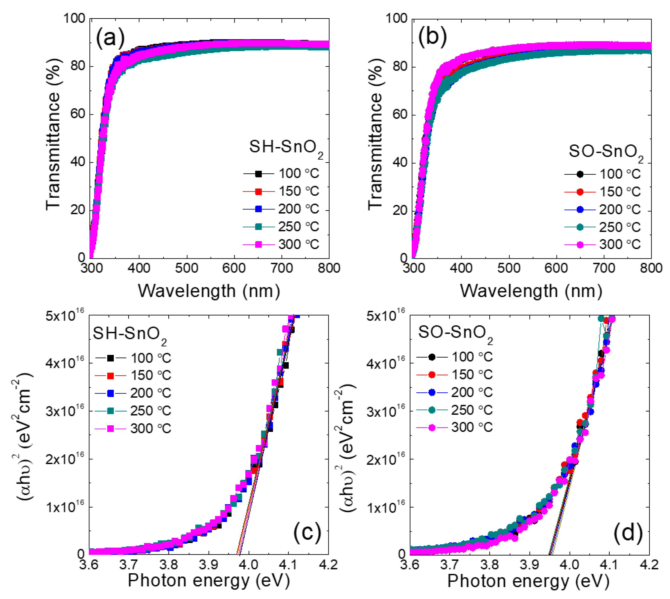
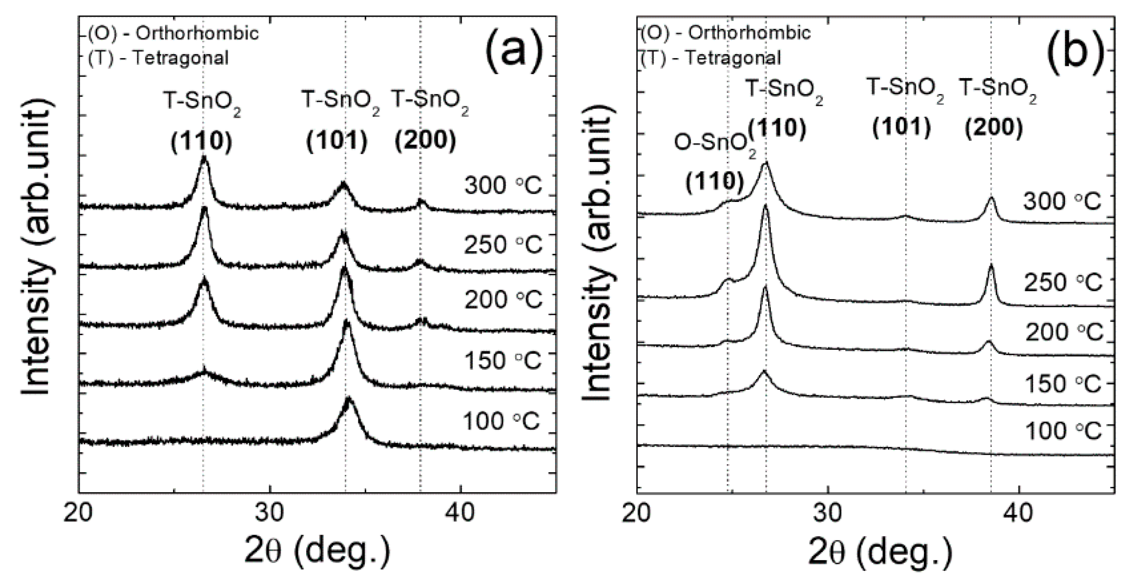
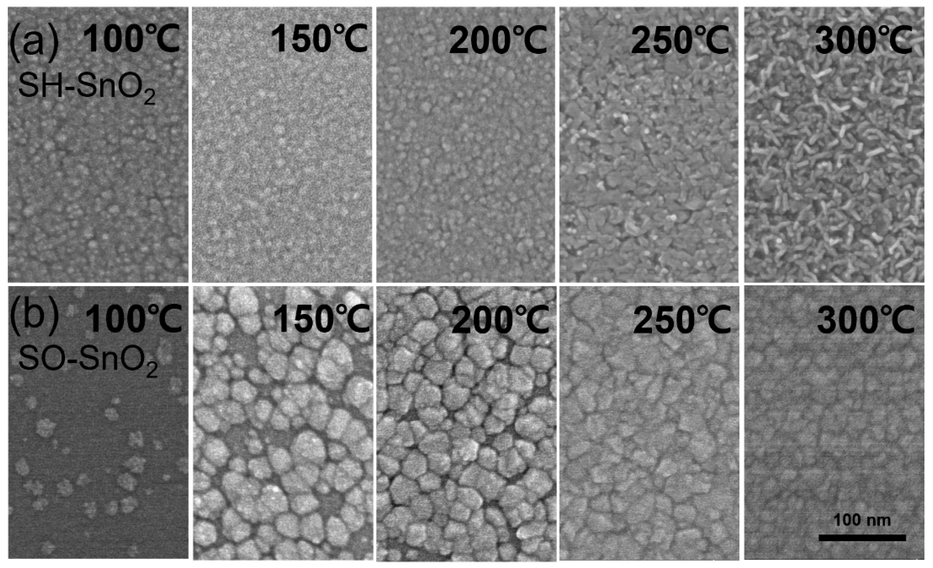
3. Results and Discussion

Figure 1a,b shows the growth characteristics of PEALD SH-SnO2 and SO-SnO2 at a deposition temperature of 200 °C. Figure 1a shows the change in the growth per cycle (GPC) of the SH-SnO2 and SO-SnO2 films by varying the Sn precursor and reactant pulse lengths. For SH-SnO2, it was found that a Sn precursor pulse length of >5 s and H2O plasma pulse length of >3 s were required to obtain the saturated GPC with self-limiting surface reaction. The optimized pulse condition was determined to be as follows: Sn precursor pulse of 6 s, N2 purge for 10 s, H2O plasma reactant pulse of 5 s, and N2 purge for 10 s. SO-SnO2 PEALD also showed the self-saturated growth characteristics for the Sn precursor and O2 plasma pulse lengths of >4 s and >3 s, respectively. As depicted in Figure 1b, both SnO2 PEALD processes show the linear increase in film thickness with increasing number of ALD cycles, and the estimated GPCs of SH-SnO2 and SO-SnO2 films are approximately 0.21 and 0.08 nm/cycle, respectively. The obtained GPC of SH-SnO2 was much higher than that of SO-SnO2 PEALD and those of previously reported SnO2 ALD from Sn(dmamp)2/O3 (0.018–0.042 nm/cycle), tetraethyltin/H2O2 (0.073–0.083 nm/cycle), Sn(edpa)2/O2 plasma (0.070 nm/cycle), TDMASn/O3 (0.10–0.16 nm/cycle), and Sn(acac)3/O3 (0.10 nm/cycle) [17,18,19,20,21]. The high GPC of SH-SnO2 PEALD might originate from the high reactivity of H2O plasma and the high density of accessible reactive sites on the surface after H2O plasma pulse. Tarlov et al. found that H2O plasma treatment on SnO2 film induced a hydroxylated surface, which may in turn act as reactive sites for subsequent Sn precursor chemisorption [22,23]. In addition, Kawamura et al. reported higher reactivity of H2O plasma than that of O2 plasma in ZnO ALD process [24].
Figure 2 shows the variations of the GPC and refractive indices of the SH-SnO2 and SO-SnO2 films as functions of deposition temperatures ranging from 100 to 300 °C. SH-SnO2 films showed a constant GPC of 0.21 nm/cycle at a wide temperature range of 100–300 °C. Refractive indices of SH-SnO2 films deposited at 100–300 °C were examined by using an ellipsometer at a wavelength of 633 nm. At the low-temperature range of 100–200 °C, the refractive index of SH-SnO2 films was 1.9, comparable with that of reported SnO2 films (1.9–2.0) [25,26,27]. By contrast, the refractive index values at the high-temperature range of 250–300 °C showed an abrupt decrease to 1.55 with increasing growth temperatures, implying the formation of less-dense SH-SnO2 films. The lower refractive index at higher deposition temperature was unexpected because previous studies reported that the density of ALD SnO2 films generally increased with deposition temperature [25,26]. The deposition of less-dense SH-SnO2 films will be discussed in detail later. For SO-SnO2 films, the GPC of 0.071–0.087 nm/cycle was obtained in the ALD temperature window of 150–250 °C. At deposition temperatures of 100 and 300 °C, the GPC values were higher than those at 150–250 °C probably due to condensation of Sn(dmamp)2 precursor and enhanced reaction kinetics between Sn(dmamp)2 and O2 plasma at 100 and 300 °C, respectively. The SO-SnO2 films showed higher GPC values than those of SnO2 films obtained from the same Sn(dmamp)2 precursor and O3 (0.017–0.042 nm/cycle) [17]. Compared with SH-SnO2, the SO-SnO2 films exhibited high refractive index values of 1.9–2.0 at all deposition temperatures, indicating the formation of dense SnO2 films irrespective of deposition temperature.
Although O2 plasma has been extensively employed as an oxidizing agent in ALD and other thin-film deposition processes, the role of H2O plasma in ALD process is still unclear because H2O plasma contains the reductive species of H2, H*, and H+, as well as the oxidative species of O2, O*, and OH [28]. Besides, Stuckert et al. and Choi et al. reported that H2O plasma treatment on SnO2 surface resulted in the reduction of SnO2 to metallic Sn, implying that H2O plasma can act as a reducing agent rather than as an oxidant [29,30]. In contrast, some previous reports on PEALD processes revealed that H2O plasma could be utilized as an oxidizing co-reactant for the growth of ZnO and TiO2 films [24,31]. Therefore, the chemical binding states and oxygen concentrations of SH-SnO2 and SO-SnO2 films must be investigated to identify the surface reaction that occurred herein. To examine the chemical binding state of both SnO2 films, XPS analysis was performed (Figure 3a,b). Sn 3d core-level XP spectra showed that the Sn 3d5/2 peaks from both PEALD films were almost identical at 486.5–486.7 eV, irrespective of the deposition temperature. This suggests the growth of pure SnO2 films (+4 oxidation state) without other sub-valent oxide phases, such as Sn2O3, SnO, and Sn, and that H2O plasma acted as an oxidizing agent rather than as a reducing agent. To measure the concentration of residual carbon and nitrogen impurities that may come from the Sn precursor, N 1s and C 1s spectra were also obtained. For SH-SnO2 films, carbon and nitrogen concentrations were below XPS detection levels at all investigated deposition temperatures. Contrarily, carbon impurities were detected for SO-SnO2 films grown at a low temperature of 100 °C, as shown in the inset of Figure 3b, attributed to the comparably lower reactivity of O2 plasma than H2O plasma.
Further chemical analysis was performed using D-SIMS, and the Sn/O ratios and hydrogen concentrations of SH-SnO2 and SO-SnO2 films deposited at 200 °C were compared. Figure 4a,b shows the compositional depth profiles of the SH-SnO2 and SO-SnO2 films, respectively. Both PEALD SnO2 films showed uniform Sn, O, and H distributions in the depth direction. Furthermore, the Sn/O intensity ratios for both SnO2 films were perfectly identical, suggesting that the SnO2 films had the same Sn:O compositions. Meanwhile, the SH-SnO2 film showed two-fold higher hydrogen intensity than that of the SO-SnO2 film due to hydrogen incorporation from H-containing species in H2O plasma. Notably, hydrogen impurity concentrations in various oxides influence the crystalline structure and electrical properties, like carrier mobility and concentrations [32,33,34]. For example, Husein et al. reported that hydrogen-doped indium oxide films showed decreased electron mobility as the hydrogen content was increased to 5.7% [33].
Figure 5 shows the optical properties of the SH-SnO2 and SO-SnO2 films grown at different deposition temperatures. Figure 5a,b presents the transmittance of the 20-nm-thick PEALD SH-SnO2 and SO-SnO2 films deposited on soda-lime glass, respectively. It was shown that all the SnO2 films have high transparencies (>80%) in the visible light range (wavelength = 350–700 nm). Figure 5c,d exhibits the optical band gaps of the SnO2 films derived from the Tauc equation (α = A (Eg)1/2 for direct band gap transition, where α is the absorption coefficient, is the photon energy, and Eg is the optical band gap) [35,36]. Optical band gaps of the SnO2 films were determined by extrapolating the graph of the linear part of the curve to the x-axis. It was confirmed that the band gap energy, regardless of the deposition temperature and plasma reactant, was almost constant at about 3.95–3.98 eV, which is in good agreement with ALD SnO2 films [7].
The crystalline structures of the 20-nm-thick SnO2 films were investigated at different deposition temperatures ranging from 100 to 300 °C. For SH-SnO2 films, distinct diffraction peaks corresponding to tetragonal rutile SnO2 (110), SnO2 (101), and SnO2 (200) were found at 26.5°, 34.0°, and 38.5° over a wide deposition temperature range of 100–300 °C, indicating the growth of polycrystalline SnO2 films (Figure 6a). The SH-SnO2 films grown at lower temperatures of 100–200 °C showed the (101) preferred orientation, while a strong (110) preferred orientation was found by increasing the deposition temperature to 300 °C. For SO-SnO2 (Figure 6b), the clear diffraction peaks at 26.5° and 38° for tetragonal SnO2 (110) and SnO2 (200), respectively, were observed at deposition temperatures of >150 °C. The SO-SnO2 films showed the (110) preferred orientation, irrespective of the deposition temperature. By contrast, amorphous SnO2 film was grown at 100 °C. By contrast to SH-SnO2, the weak diffraction peak at 24.8°, which corresponds to orthorhombic columbite SnO2 (110), was observed for SO-SnO2, and the relative intensity of orthorhombic SnO2 peak increases with growth temperature. It should be noted that the growth of less-stable orthorhombic SnO2 by ALD has been rarely reported. Kim et al. observed an orthorhombic SnO2 phase by epitaxial PEALD on yttria-stabilized zirconia substrate [37].
Figure 7a shows the plane-view high-resolution FESEM images of the SH-SnO2 films deposited at 100–300 °C. Despite the low deposition temperature of 100 °C, the SH-SnO2 film showed a small and dense nanocrystalline structure. At deposition temperatures up to 200 °C, the grain size of the SH-SnO2 films were approximately 15–20 nm, and a dense SnO2 surface was observed. By contrast, SnO2 films became less dense and rougher on increasing the temperature beyond 250 °C, and eventually the SH-SnO2 films showed significantly porous structures with rod-shaped crystallites at 300 °C. The formation of porous nanostructured SnO2 is consistent with the noticeably low refractive index of the SH-SnO2 films grown at 250 °C and 300 °C. Although it is very tricky to reveal the complicated surface reactions during PEALD of SH-SnO2, the morphology change of the SnO2 films from smooth SnO2 surface to rod-shaped porous structure at deposition temperatures of >250 °C might be ascribed to the partial reduction of SnO2 to Sn metal by reductive H-containing species in H2O plasma, followed by thermal etching via Sn evaporation or agglomeration of the Sn metal. It has been reported that H2O plasma treatment on SnO2 film resulted in a morphological change to nanoglobular structure due to reduction of SnO2 to Sn [29]. At the higher growth temperature of >350 °C, SH-SnO2 resulted in more porous surface due to much severe reduction of SnO2 and Sn evaporation/agglomeration (data not shown here). Figure 7b shows the plane-view images of the SO-SnO2 films grown at temperatures of 100–300 °C. The SO-SnO2 film grown at 100 °C showed an amorphous phase and merely a few crystallites scattered in the amorphous film. On increasing the deposition temperature to 250 °C, the SO-SnO2 films showed dense and large polygonal grains of size ~50 nm, while the SO-SnO2 film grown at 300 °C showed a dense and polycrystalline structure with decreased grain size. The formation of dense SO-SnO2 thin films at deposition temperatures of 250 °C and 300 °C is well matched with the high refractive index of ~2.0 obtained from an ellipsometer.
Hall-effect measurements were performed to investigate the electrical properties of the PEALD of SnO2 films at room temperature. SnO2 films (20-nm thick) were deposited on soda-lime glass using both H2O plasma and O2 plasma at 100–300 °C, and indium was used for the ohmic contact on the four vertexes. First, it was confirmed that all the PEALD SnO2 films exhibited n-type carrier behavior, i.e., the majority carrier was electrons, regardless of the deposition temperature. Figure 8a,b shows the carrier concentrations, Hall mobilities, and resistivities of the SH-SnO2 and SO-SnO2 films, respectively. SH-SnO2 films grown at 100–300 °C have moderate carrier concentration of approximately 1 × 10¹⁷–30 × 1017 cm−3 and rather low electrical mobility of 0.4–1.5 cm2 V−1·s−1. The low Hall mobilities of the SH-SnO2 thin films could be explained by the significant grain boundary scattering due to the small grain structure and high grain boundary density, as observed in the FESEM images. Resistivities of the SH-SnO2 films grown at 100–150 °C were ~5 Ω·cm, and it gradually increased to 7–38 Ω·cm for the SH-SnO2 films grown at 200–300 °C, attributed to the porous SnO2 structures (Figure 7a). For polycrystalline SO-SnO2 films grown at 100–300 °C, higher carrier concentrations of 7 × 10¹⁸–4 × 1019 cm−3 were obtained. The SO-SnO2 films grown at 100 °C showed Hall mobilities of ~5.8 cm2 V−1·s−1, which continually increased to 27 cm2 V−1·s−1 as the deposition temperature was raised to 250 °C, along with the lowest resistivity of 6 × 10⁻³ Ω·cm. This was evidenced by the larger and denser grains obtained at the high deposition temperature of 250 °C.

4. Conclusions

In this study, SnO2 PEALD processes over a wide growth temperature range of 100–300 °C using different plasma sources, either H2O plasma or O2 plasma, were demonstrated, and their growth behavior and film properties were compared. SnO2 films grown from H2O plasma (SH-SnO2) showed a higher growth rate of 0.21 nm/cycle than that of SnO2 films grown from O2 plasma (SO-SnO2) due to the stronger reactivity of H2O plasma and more OH-reactive sites. The SH-SnO2 films showed negligible carbon and nitrogen impurities at all deposition temperatures from 100 to 300 °C, but they contained two-fold higher hydrogen concentrations than the SO-SnO2 films. The SO-SnO2 featured dense and uniform surface morphology with relatively larger grain size, while SH-SnO2 showed nanocrystallites with small grain size at moderate temperatures, and porous rod-shaped structures at higher deposition temperatures of 250 and 300 °C. At 250 °C, the SO-SnO2 film showed high carrier concentration of ~4 × 1019 cm−3 and high Hall mobility of 27 cm2 V−1·s−1. By contrast, the SH-SnO2 films showed poorer conductivity, lower carrier concentration, and lower Hall mobility than the SO-SnO2 films at all deposition temperatures, probably due to the significant grain boundary scattering and hydrogen impurity scattering within the SH-SnO2 films.

Author Contributions

Conceptualization, J.H.W. and J.H.H.; investigation, J.H.W. and J.H.H.; resources, S.H.H., B.K.P. and T.-M.C.; writing—original draft preparation, J.H.W. and J.H.H.; writing—review and editing, J.H.W. and J.H.H.; supervision, J.H.H.; project administration, J.H.H. All authors have read and agreed to the published version of the manuscript.

Funding

This study was supported by the Research Program funded by the SeoulTech (Seoul National University of Science and Technology).

Conflicts of Interest

The authors declare no conflict of interest.

References

  1. Paulowicz, I.; Hrkac, V.; Kaps, S.; Cretu, V.; Lupan, O.; Braniste, T.; Duppel, V.; Tiginyanu, I.; Kienle, L.; Adelung, R. Three-dimensional SnO2 nanowire networks for multifunctional applications: From high-temperature stretchable ceramics to ultra responsive sensors. Am. Ceram. Soc. Bull. 2015, 94, 21. [Google Scholar]
  2. Guan, C.; Wang, X.; Zhang, Q.; Fan, Z.; Zhang, H.; Fan, H.J. Highly stable and reversible lithium storage in SnO2 nanowires surface coated with a uniform hollow shell by atomic layer deposition. Nano Lett. 2014, 14, 4852–4858. [Google Scholar] [CrossRef]
  3. Kim, D.H.; Shin, D.Y.; Lee, Y.G.; An, G.H.; Han, J.H.; Ahn, H.J.; Choi, B.J. Effects of SnO2 layer coated on carbon nanofiber for the methanol oxidation reaction. Ceram. Int. 2018, 44, 19554–19559. [Google Scholar] [CrossRef]
  4. Park, M.; Kim, J.Y.; Son, H.J.; Lee, C.H.; Jang, S.S.; Ko, M.J. Low-temperature solution-processed Li-doped SnO2 as an effective electron transporting layer for high-performance flexible and wearable perovskite solar cells. Nano Energy 2016, 26, 208–215. [Google Scholar] [CrossRef]
  5. Chu, H.C.; Shen, Y.S.; Hsieh, C.H.; Huang, J.H.; Wu, Y.H. Low-voltage operation of ZrO2-gated n-type thin-film transistors based on a channel formed by hybrid phases of SnO and SnO2. ACS Appl. Mater. Interfaces 2015, 7, 15129–15137. [Google Scholar] [CrossRef]
  6. Jarzebski, Z.M.; Marton, J.P. Physical properties of SnO2 materials. J. Electrochem. Soc. 1976, 123, 299–310. [Google Scholar] [CrossRef]
  7. Manifacier, J.C.; De Murcia, M.; Fillard, J.P.; Vicario, E. Optical and electrical properties of SnO2 thin films in relation to their stoichiometric deviation and their crystalline structure. Thin Solid Films 1977, 41, 127–135. [Google Scholar] [CrossRef]
  8. Minami, T.; Nanto, H.; Takata, S. Highly conducting and transparent SnO2 thin films prepared by RF magnetron sputtering on low-temperature substrates. Jpn. J. Appl. Phys. 1988, 27, L287–L289. [Google Scholar] [CrossRef]
  9. Liu, Y.; Koep, E.; Liu, M. A highly sensitive and fast-responding SnO2 sensor fabricated by combustion chemical vapor deposition. Chem. Mater. 2005, 17, 3997–4000. [Google Scholar] [CrossRef]
  10. Korotcenkov, G.; Brinzari, V.; Schwank, J.; Dibattista, M.; Asiliev, A. Peculiarities of SnO2 thin film deposition by spray pyrolysis for gas sensor application. Sens. Actuators B 2001, 77, 244–252. [Google Scholar] [CrossRef]
  11. Kim, H.; Piqué, A. Transparent conducting Sb-doped SnO2 thin films grown by pulsed-laser deposition Transparent conducting Sb-doped SnO2 thin films grown by pulsed-laser deposition. Appl. Phys. Lett. 2004, 218, 10–13. [Google Scholar]
  12. Lu, J.; Sundqvist, J.; Ottosson, M.; Tarre, A.; Rosental, A.; Aarik, J.; Hårsta, A. Microstructure characterisation of ALD-grown epitaxial SnO2 thin films. J. Cryst. Growth. 2004, 260, 191–200. [Google Scholar] [CrossRef]
  13. George, S.M. Atomic layer deposition: An overview. Chem. Rev. 2010, 110, 111–131. [Google Scholar] [CrossRef] [PubMed]
  14. Johnson, R.W.; Hultqvist, A.; Bent, S.F. A brief review of atomic layer deposition: From fundamentals to applications. Mater. Today. 2014, 17, 236–246. [Google Scholar] [CrossRef]
  15. Wang, C.; Zhao, D.; Grice, C.R.; Liao, W.; Yu, Y.; Cimaroli, A.; Shrestha, N.; Roland, P.J.; Chen, J.; Yu, Z.; et al. Low-temperature plasma-enhanced atomic layer deposition of tin oxide electron selective layers for highly efficient planar perovskite solar cells. J. Mater. Chem. A. 2016, 4, 12080–12087. [Google Scholar] [CrossRef]
  16. Lee, D.K.; Wan, Z.; Bae, J.S.; Lee, H.B.R.; Ahn, J.H.S.; Kim, D.; Kim, J.; Kwon, S.H. Plasma-enhanced atomic layer deposition of SnO2 thin films using SnCl4 and O2 plasma. Mater. Lett. 2016, 166, 163–166. [Google Scholar] [CrossRef]
  17. Choi, M.J.; Cho, C.J.; Kim, K.C.; Pyeon, J.J.; Park, H.H.; Kim, H.S.; Han, J.H.; Kim, C.G.; Chung, T.M.; Park, T.J.; et al. SnO2 thin films grown by atomic layer deposition using a novel Sn precursor. Appl. Surf. Sci. 2014, 320, 188–194. [Google Scholar] [CrossRef]
  18. Lim, S.S.; Baek, I.H.; Kim, K.C.; Baek, S.H.; Park, H.H.; Kim, J.S.; Kim, S.K. Atomic layer deposition of SnO2 thin films using tetraethyltin and H2O2. Ceram. Int. 2019, 45, 20600–20605. [Google Scholar] [CrossRef]
  19. Kim, H.Y.; Nam, J.H.; George, S.M.; Park, J.S.; Park, B.K.; Kim, G.H.; Jeon, D.J.; Chung, T.M.; Han, J.H. Phase-controlled SnO2 and SnO growth by atomic layer deposition using Bis(N-ethoxy-2,2-dimethyl propanamido)tin precursor. Ceram. Int. 2019, 45, 5124–5132. [Google Scholar] [CrossRef]
  20. won Choi, D.; Park, J.S. Highly conductive SnO2 thin films deposited by atomic layer deposition using tetrakis-dimethyl-amine-tin precursor and ozone reactant. Surf. Coatings Technol. 2014, 259, 238–243. [Google Scholar] [CrossRef]
  21. Chang, S.; Selvaraj, S.K.; Choi, Y.-Y.; Hong, S.; Nakhmanson, S.M.; Takoudis, C.G. Atomic layer deposition of environmentally benign SnTiOx as a potential ferroelectric material. J. Vac. Sci. Technol. A 2016, 34, 01A119. [Google Scholar] [CrossRef] [Green Version]
  22. Tarlov, M.J.; Evans, J.F.; Newman, J.G. Static SIMS and XPS study of water plasma exposed tin oxide films. Appl. Surf. Sci. 1993, 64, 115–125. [Google Scholar] [CrossRef]
  23. Tarlov, M.J.; Evans, J.F. Surface characterization of radio frequency water plasma treated and annealed polycrystalline tin oxide thin films. Chem. Mater. 1990, 2, 49–60. [Google Scholar] [CrossRef]
  24. Kawamura, Y.; Hattori, N.; Miyatake, N.; Uraoka, Y. Comparison between ZnO films grown by plasma-assisted atomic layer deposition using H2O plasma and O2 plasma as oxidant. J. Vac. Sci. Technol. A. 2013, 31, 01A142. [Google Scholar] [CrossRef]
  25. Heo, J.; Kim, S.B.; Gordon, R.G. Atomic layer deposition of tin oxide with nitric oxide as an oxidant gas. J. Mater. Chem. 2012, 22, 4599–4602. [Google Scholar] [CrossRef] [Green Version]
  26. Heo, J.; Hock, A.S.; Gordon, R.G. Low temperature atomic layer deposition of tin oxide. Chem. Mater. 2010, 22, 4964–4973. [Google Scholar] [CrossRef]
  27. Patnaik, P. Handbook of Inorganic Chemicals; McGraw-Hill Companies, Inc.: New York, NY, USA, 2003; p. 940. ISBN 0-07-049439-8. [Google Scholar]
  28. Stuckert, E.P.; Miller, C.J.; Fisher, E.R. Gas-phase diagnostics during H2 and H2O plasma treatment of SnO2 nanomaterials: Implications for surface modification. J. Vac. Sci. Technol. B 2017, 35, 021802. [Google Scholar] [CrossRef]
  29. Stuckert, E.P.; Fisher, E.R. Ar/O2 and H2O plasma surface modification of SnO2 nanomaterials to increase surface oxidation. Sens. Actuators B Chem. 2015, 208, 379–388. [Google Scholar] [CrossRef]
  30. Choi, M.S.; Lee, Y.J.; Kwon, J.D.; Jeong, Y.; Park, J.Y.; Kang, Y.C.; Song, P.K.; Kim, D.H. Effects of hydrogen plasma treatment on SnO2:F substrates for amorphous Si thin film solar cells. Curr. Appl. Phys. 2013, 13, 1589–1593. [Google Scholar] [CrossRef]
  31. Xie, Q.; Musschoot, J.; Deduytsche, D.; Van Meirhaeghe, R.L.; Detavernier, C.; Van Den Berghe, S.; Jiang, Y.L.; Ru, G.P.; Li, B.Z.; Qu, X.P. Growth kinetics and crystallization behavior of TiO2 films prepared by plasma enhanced atomic layer deposition. J. Electrochem. Soc. 2008, 155, 688–692. [Google Scholar] [CrossRef]
  32. Dymond, E.G. Scattering of electrons in helium. Nature 1926, 118, 336–337. [Google Scholar] [CrossRef]
  33. Husein, S.; Stuckelberger, M.; West, B.; Ding, L.; Dauzou, F.; Morales-Masis, M.; Duchamp, M.; Holman, Z.; Bertoni, M.I. Carrier scattering mechanisms limiting mobility in hydrogen-doped indium oxide. J. Appl. Phys. 2018, 123, 245102. [Google Scholar] [CrossRef]
  34. Villamagua, L.; Stashans, A.; Carini, M.; Maldonado, F. Doping of SnO2 with H atoms: An alternative way to attain n-type conductivity. AIP Adv. 2016, 6, 115217. [Google Scholar] [CrossRef] [Green Version]
  35. Baco, S.; Chik, A.; Yassin, F.M. Study on optical properties of tin oxide thin film at different annealing temperature. J. Sci. Technol. 2012, 4, 61–72. [Google Scholar]
  36. Tauc, J.C. Optical Properties of Solid; Abeles, F., Ed.; North-Holland Publishing: Amsterdam, The Netherlands, 1972; p. 279. [Google Scholar]
  37. Kim, S.; Kim, D.-H.; Hong, S.-H. Epitaxial growth of orthorhombic SnO2 films on various YSZ substrates by plasma enhanced atomic layer deposition. J. Cryst. Growth 2012, 348, 15–19. [Google Scholar] [CrossRef]
Figure 1. (a) Variations in the growth per cycle (GPC) of SH-SnO2 and SO-SnO2 plasma-enhanced atomic layer deposition (PEALD) processes at 200 °C, depending on the Sn source and reactant pulse lengths. (b) Change in SnO2 thicknesses with increasing number of SH-SnO2 and SO-SnO2 PEALD cycles.
Coatings 10 00692 g001
Figure 2. GPC and refractive index of the SnO2 thin films deposited at 100–300 °C using (a) Sn(dmamp)2/H2O plasma and (b) Sn(dmamp)2/O2 plasma.
Coatings 10 00692 g002
Figure 3. Sn 3d XPS core level spectra of the SnO2 films deposited at 100–300 °C using (a) Sn(dmamp)2/H2O plasma and (b) Sn(dmamp)2/O2 plasma. Inset of Figure 3b shows the C 1s X-ray photoelectron (XP) spectra of SO-SnO2 films.
Coatings 10 00692 g003
Figure 4. Dynamic secondary ion mass spectrometry (D-SIMS) depth profiles of (a) SH-SnO2 and (b) SO-SnO2 films deposited at 200 °C.
Coatings 10 00692 g004
Figure 5. Optical transmittance of 20-nm-thick (a) SH-SnO2 films and (b) SO-SnO2 films deposited on a soda-lime glass substrate at 100–300 °C. Optical band gaps of (c) SH-SnO2 and (d) SO-SnO2 films grown at 100–300 °C.
Coatings 10 00692 g005
Figure 6. Glancing-angle X-ray diffraction (GAXRD) patterns of (a) SH-SnO2 and (b) SO-SnO2 thin films deposited at different temperatures of 100, 150, 200, 250, and 300 °C.
Coatings 10 00692 g006
Figure 7. Plane-view high-resolution FESEM images of (a) SH-SnO2 and (b) SO-SnO2 films grown at deposition temperatures of 100–300 °C.
Coatings 10 00692 g007
Figure 8. Carrier concentrations, Hall mobilities, and resistivities of (a) SH-SnO2 and (b) SO-SnO2 films as a function of growth temperature.
Coatings 10 00692 g008

